Electronics Production
Zach's Information, Notes, Documentation, etc. for w08 will live here. Please click on the collapsibles to view more detailed information. In each of the sections, more information about the Process, Improvements to Worflow, General Takeaways, Research, and any Necessary Files.The distance between insanity and genius is measured only by success — Bruce Feirstein
Plan/Dates W08:
- Wednesday 3/12/25 EOD:
- KiCaD Day 1
- In-work Time Request: 1-1.5 hours
- Thursday 3/13/25 EOD:
- KiCaD Day 2
- In-work Time Request: 1.5-2 hours
- Friday 3/14/25 EOD:
- Board Milling Day 1
- Saturday 3/15/25 EOD:
- Board Milling Day 2
- XTool F1 Day 1
- Sunday 3/16/25 EOD:
- Soldering (Hopefully Day 1)
- Board testing Day 1
- Monday 3/17/25 EOD:
- Soldering (If necessary)
- Board testing Day 2
- Have 75% of documentation finalized by 14:00 EST
- Tuesday 3/18/25 EOD:
- Catch-up day and documentation finalization
Plan/Dates W10:
- Thursday 3/27/25 EOD:
- OOO for PTO
- Friday 3/28/25 EOD:
- OOO for PTO
- Watch Recorded FAB Lecture
- Saturday 3/29/25 EOD:
- OOO for PTO
- Design PCB using KiCAD
- Sunday 3/30/25 EOD:
- OOO for PTO
- Travel day - back from SEA TAC/PHL to CMH
- Monday 3/31/25 EOD:
- Finish/Finalize PCB Design
- Requested In-Work Time
- CNC/Laser Cut PCB
- Tuesday 4/1/25 EOD:
- Soldering Day 1
- Finalize Documentation begin W09 Catch-up
- Wednesday 4/2/25 EOD:
- Finish Soldering (Day 2) and Test
- Finalize Documentation continue W09 Catch-up
Plan/Dates:
- Thursday 3/20/25 EOD:
- Decide on input devices
- Finalize KiCAD File
- Friday 3/21/25 EOD:
- Gone CMH → SEA-TAC
- Saturday 3/22/25 EOD:
- OOO
- Sunday 3/23/25 EOD:
- OOO
- Monday 3/24/25 EOD:
- OOO
- Tuesday 3/25/25 EOD:
- OOO
Tasks This Week:
Group assignments:
- Characterize the design rules for your in-house PCB production process
- Submit a PCB design to a board house
Individual assignments:
- Make and test a microcontroller development board that you designed
- Extra credit: make it with another process
Below, I walk through some of the notes/screenshots that I have from my work this week and explain my thought process as I was completing my assignments.
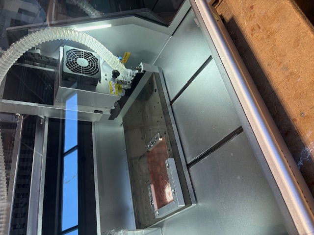
- We have at multiple options for milling at my FAB Lab. For this week, I am using the Carvera CNC machine and the Xtool F1 Ultra Laser are present, but only the Carvera CNC will work for this purpose because the XTool's Laser is not functioning correctly
- To start download the Makera CAM and the Carvera Controller
- For my Tools: 1/64 end mill, 10 degree engraving bit, 15 degree engraving bit
- For my Material: FR-1 PCB Board
- I prepared my files for the Carvera using MODS
- I took the KiCAD File from the board that I made in the past few weeks (a basic board with some pinouts) and milled it using the Carvera
- One of the best parts about the workflow for the Carvera is that because of its autoleveling feature, setting up the toolpath is essentially as simple as plugging in a PNG or SVG of your board and (more or less) just hitting "go." (This also helps to alleviate the issue of breaking copious numbers of bits)
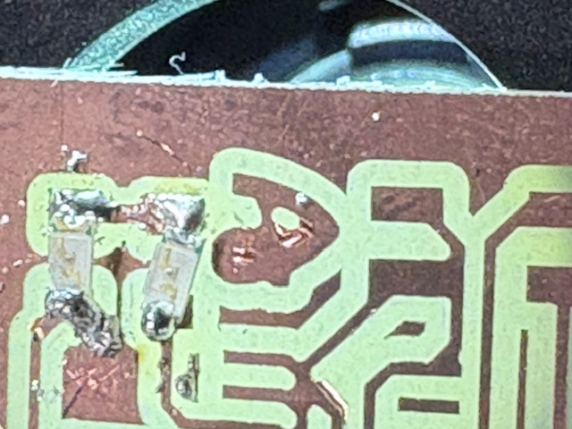
- After I pulled everything off of the Carvera, I moved on to soldering. Because this was my first ever experience with Soldering I took a board from Adrian's site on networking, milled it, and found all of the components necessary (a capacitor, 3 and 6 pinout, an LED, and a transistor) and began to practice my Soldering on that before I moved on to my own board
- This practice took MUCH longer than I anticipated and because of a scheduling issue for me, I was not able to finish the soldering and testing of my own board. That said, I did test my connections on Adrian's boards and they worked well.
- I did, however, get a chance to test my updated board, at least approximately in Wokwi before I started soldering to make sure that my board (namely the LEDs that I was going to be blinking) and code, at least in theory, would work correctly.
- 3-19-25 Update: I will have everything soldered and tested for my own board by the EOW this week.


- The obvious first improvement to my workflow would be that I should have alotted more time for Soldering and testing my board. Frankly, I just was not exactly sure what I was getting into with the soldering when I started and the process took me so, so much longer to figure out than I thought.
- One of the next improvements that I would make to my workflow would be to CAD a case for the finished and tested boards - this would allow me to have a bit more peace of mind when moving them around.
- Try not to overthink the whole process - take each step one at a time
- Always budget more time for catch up than seems necessary at the beginning of the week
- Soldering sucks/is very tedious. Having a clean work environment and some quiet for concentration are very helpful.
- For the final project, I will obviously need to solder, but one of the things that I need to do for that project will be to think about what surface I want to attach my board to. If things go as planned, which is obviously not guaranteed, I may want to think about using a flexible board.