WEEK 6: Electronics Design
Assignment - PCB Design and Circuit Implementation
1. PCB Design in KiCad - USB Connector Circuit
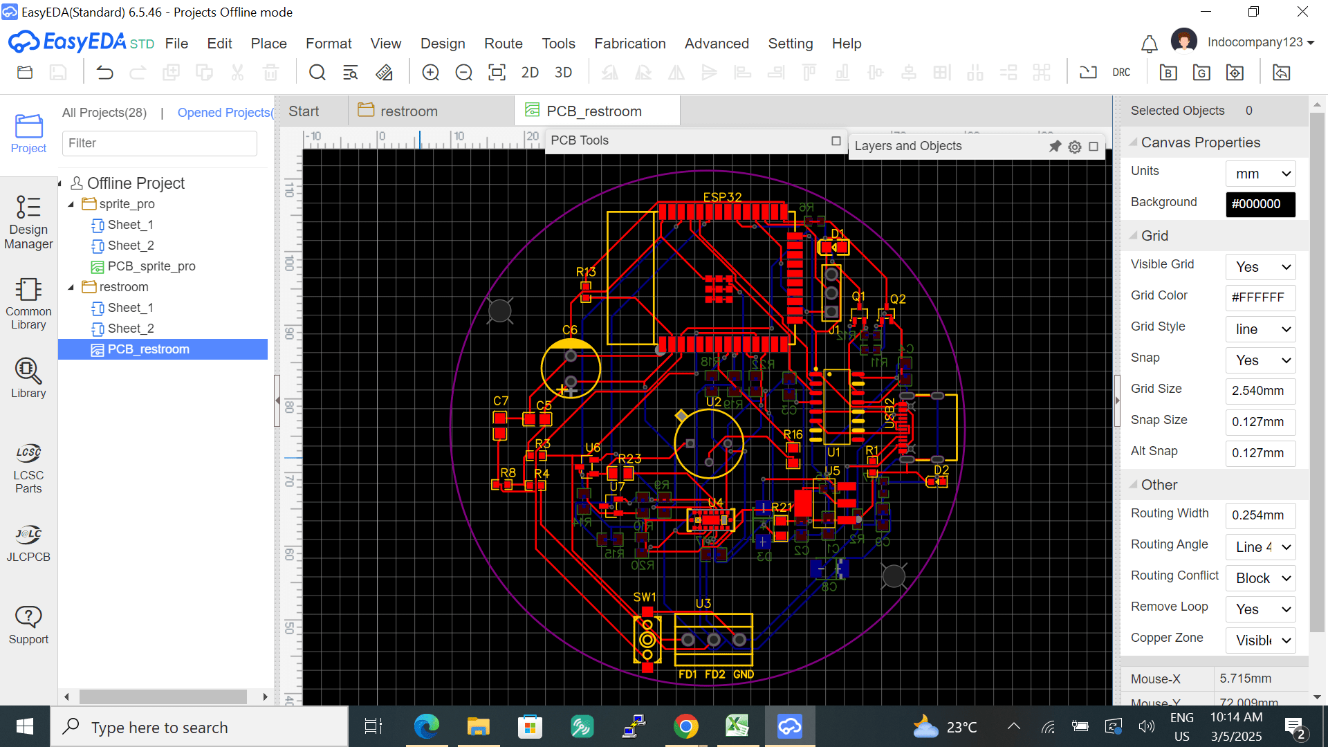
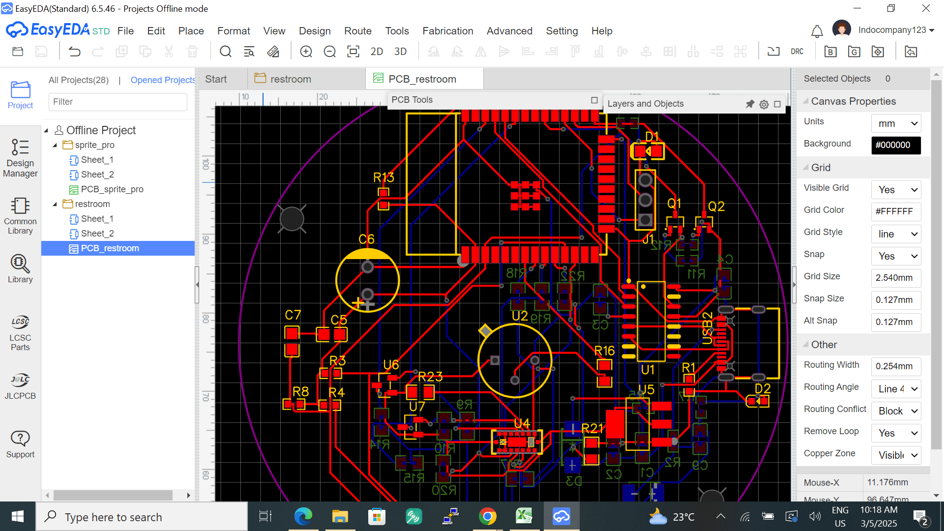
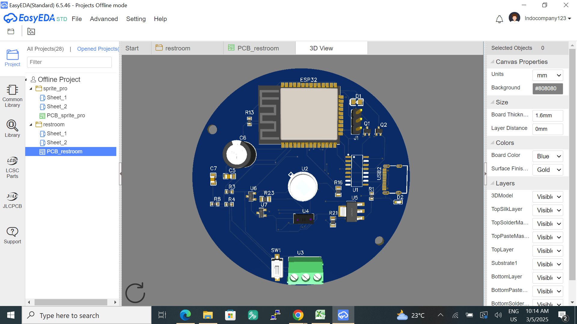
2. PCB Design in EasyEDA - ESP32-Based Circuit with ToF Sensor
Basics of Electronics
Electronics is the branch of physics and engineering that deals with the study and control of electrical energy, mainly using circuits made up of various components. It focuses on the flow of electrons through conductors, semiconductors, and insulators.
Basic Electronics Components
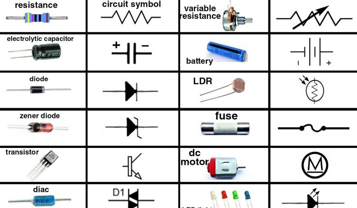
Resisters
-> Limits the flow of current in a circuit.
-> Measured in Ohms (Ω).
-> Example - Used in LED circuits to prevent excessive current.
Capacitor (C)
-> Stores electrical energy temporarily and releases it when needed.
-> Measured in Farads (F).
-> Example: Used in power supplies to smooth voltage fluctuations.
Inductor (L)
-> Stores energy in a magnetic field when current flows through it.
-> Measured in Henry (H).
-> Example: Used in transformers and filters.
Diode
-> Allows current to flow in only one direction.
-> Example: Used in rectifiers to convert AC to DC.
Transistor
-> Acts as a switch or amplifier.
-> Types: Bipolar Junction Transistor (BJT) and Field Effect Transistor (FET).
-> Example: Used in signal amplification and digital circuits.
Integrated Circuit (IC)
-> A small chip containing multiple electronic components.
-> Example: Microcontrollers, operational amplifiers (Op-Amps).
LED (Light Emitting Diode)
-> Emits light when current flows through it.
-> Example: Indicator lights in devices.
Switch
-> AProvides DC power to circuits.
-> Example: On/Off switch in electrical appliances.
Battery
-> Provides DC power to circuits.
-> Example: Used in remote controls, mobile devices, etc.
Transformer
-> Converts AC voltage levels (step-up or step-down).
-> Example: Used in power adapters.
Assignemnt
Objective
The purpose of this assignment is to design and analyze PCB circuits using KiCad and EasyEDA. The circuits involve different power supplies (5V and 12V) and various components such as microcontrollers, sensors, voltage regulators, and passive components.
Software Used
1. KiCad: Designed a USB connector-based circuit using ATtiny85.
2. EasyEDA: Designed an ESP32-based circuit with a ToF sensor and voltage regulation.
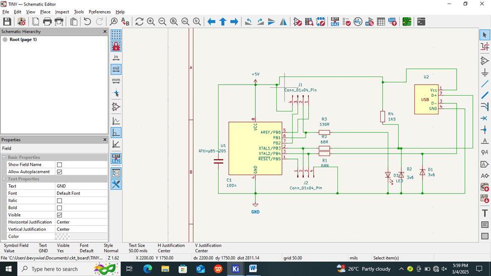
Part 1: PCB Design in KiCad (USB Connector Circuit)
Creating Schematic Diagram
Component Selection
1. Microcontroller: ATtiny85-20S
2. Passive Components: Resistors, Capacitors
3. Protection Components: Zener Diodes
4. Indicators: LED
5. Power Source: 5V
Schematic Editor
1. Open the Schematic Editor (Eeschema).
2. Add components using the "Place Symbol" tool.
3. Assign values and labels to components.
4. Connect components using wires.
5. Use labels for organized wiring.
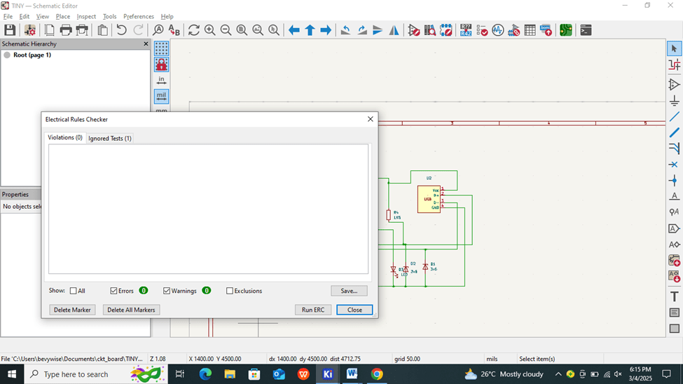
6. Perform Electrical Rule Check (ERC) to ensure proper connections.
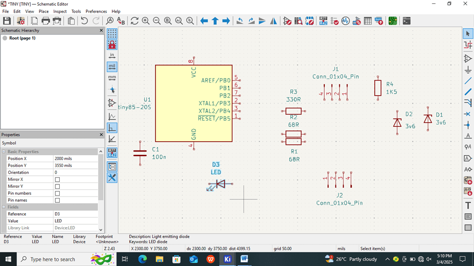
Creating Custom Parts
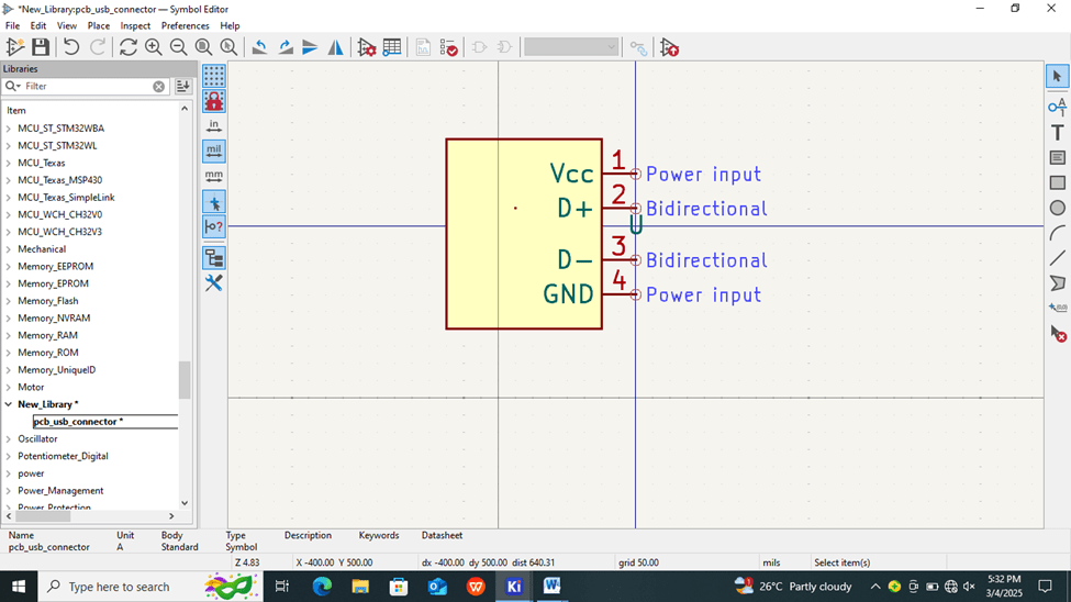
Creating a Custom Symbol
1. Open the "Symbol Editor."
2. Create a new library and add a new symbol.
3. Define pins and properties.
4. Save the symbol and link it to the schematic.
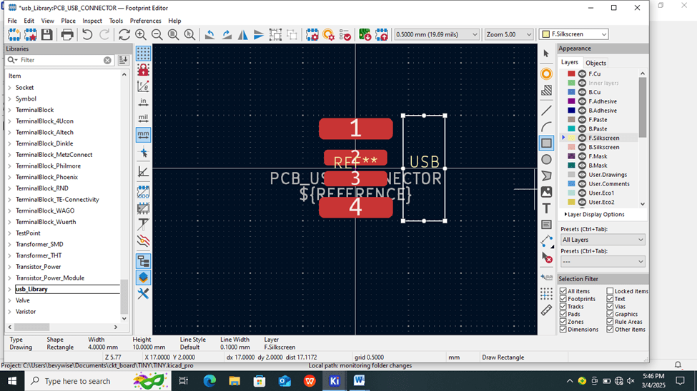
Creating a Custom Footprint
1. Open the "Footprint Editor."
2. Create a new footprint library.
3. Define pad sizes, positions, and shape.
4. Add silkscreen, courtyards, and reference designators.
5. Save the footprint and link it to the component.
Schematic Design & ERC Verification
-> Created a complete USB circuit schematic ensuring correct connections.
-> Used Electrical Rule Checker (ERC) to validate the schematic.
PCB Layout & Routing
The PCB layout design is performed by transferring the schematic components onto the PCB Editor. Proper placement of components is crucial for optimizing routing and signal integrity. After arranging components, the routing process begins, where electrical connections are made using copper traces. KiCad’s Design Rules Check (DRC) helps in verifying correct routing and ensuring compliance with spacing and manufacturing constraints. For multi-layer boards, via placement is essential to maintain signal flow between layers. After routing is completed, the design is visually inspected for errors.
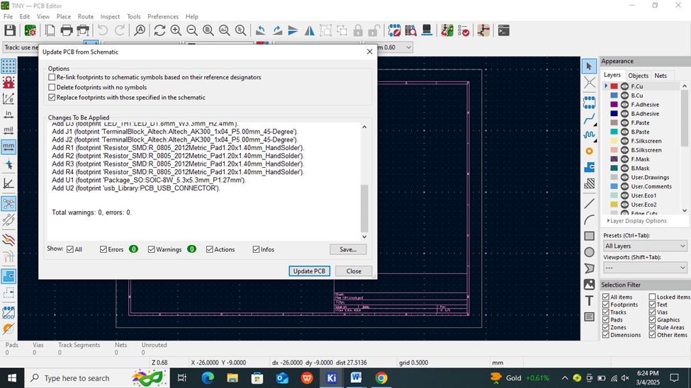
Import Netlist to PCB Editor
1. Open "PCB Editor (Pcbnew)."
2. Import the Netlist to load components.
3. Arrange components for optimal layout.
4. Use "Edge.Cuts" layer to define board shape.
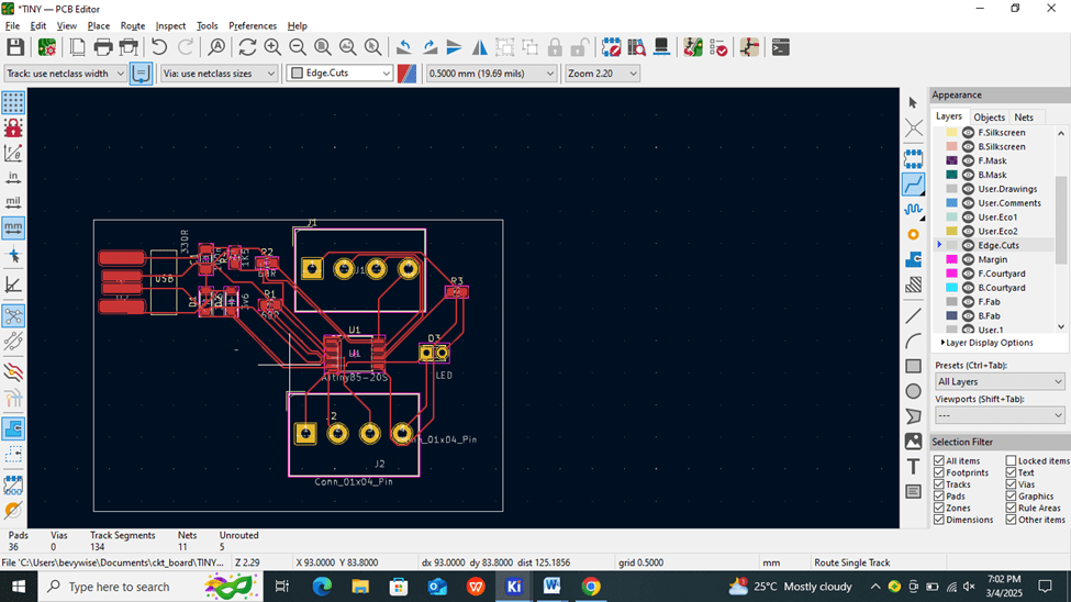
Routing the PCB
1. Set design rules (track width, clearance, via size).
2. Route traces manually or use the auto-router.
3. Ensure power and ground planes are properly connected.
3D Viewer of PCB Board
1. Open the 3D Viewer tool in KiCad.
2. Inspect the PCB in 3D to ensure proper placement and alignment.
3. Rotate and zoom to check for clearance and silkscreen positioning.
Generating Gerber Files for Manufacturing
To manufacture the PCB, Gerber files are generated, which include copper layers, solder mask, and silkscreen details. Additionally, a drill file is produced for hole placement. Before sending the design for fabrication, a 3D view is examined to verify component alignment and board structure. Once the design is finalized, the files are sent to a PCB manufacturer for production.
Generate Gerber Files
1 Open "Plot" in the PCB Editor.
2. Select the required layers (Top, Bottom, Silkscreen, Mask, Edge.Cuts).
3. Click "Plot" to generate Gerber files.
4. Open "Generate Drill Files."
5. Set correct settings and export drill file.
6. Use Gerber Viewer to check file correctness.
Gerber Files
Part 2: PCB Design in EasyEDA (ESP32-Based Circuit with ToF Sensor)
Component Selection
1. Microcontroller: ESP32
2. Sensors: ToF Sensor
3. Power Regulation: Voltage Regulator
4. Passive Components: Resistors, Capacitors, Inductor
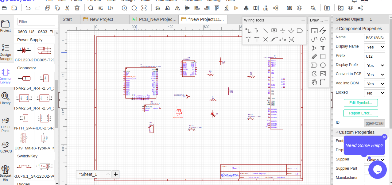
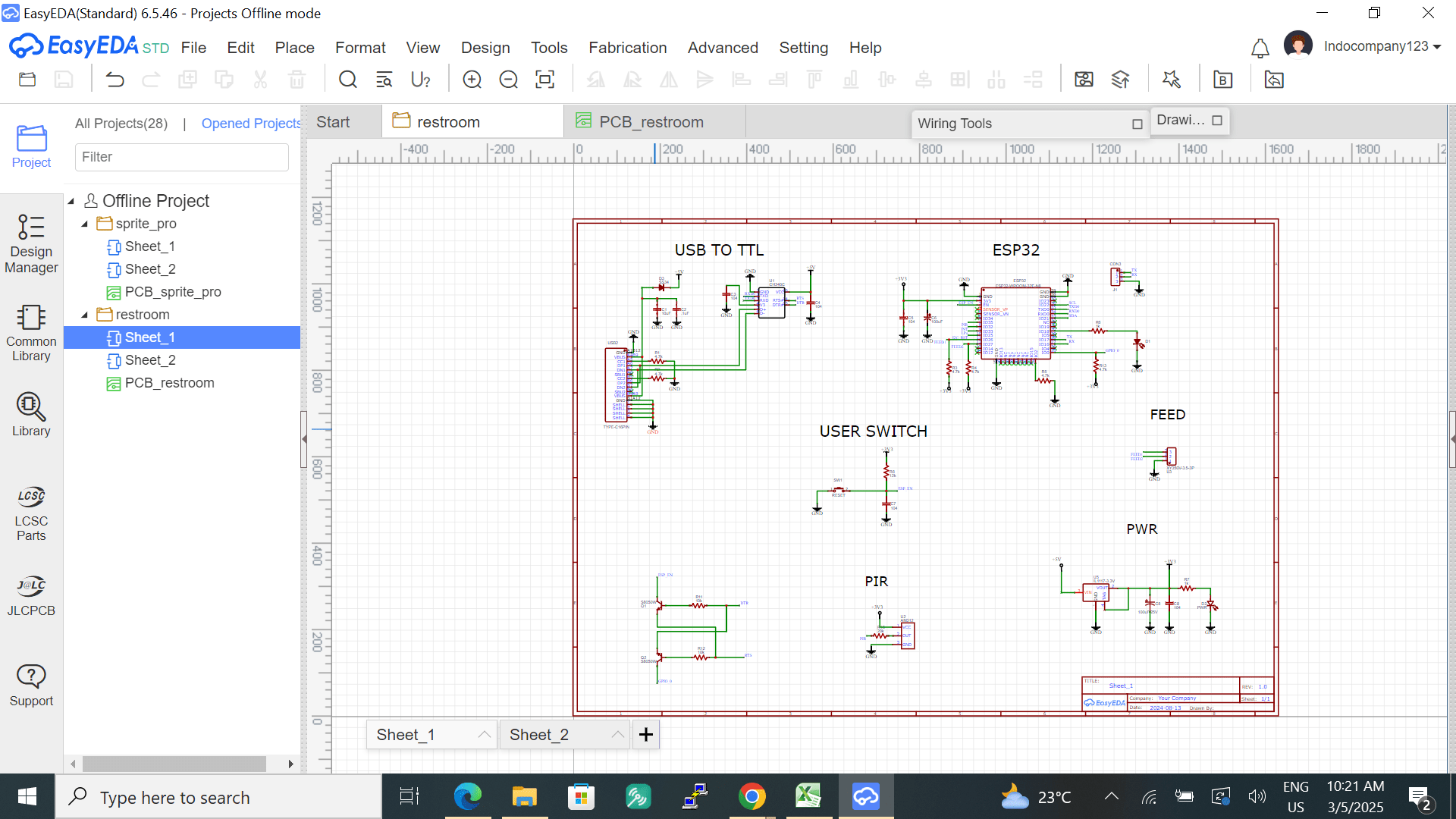
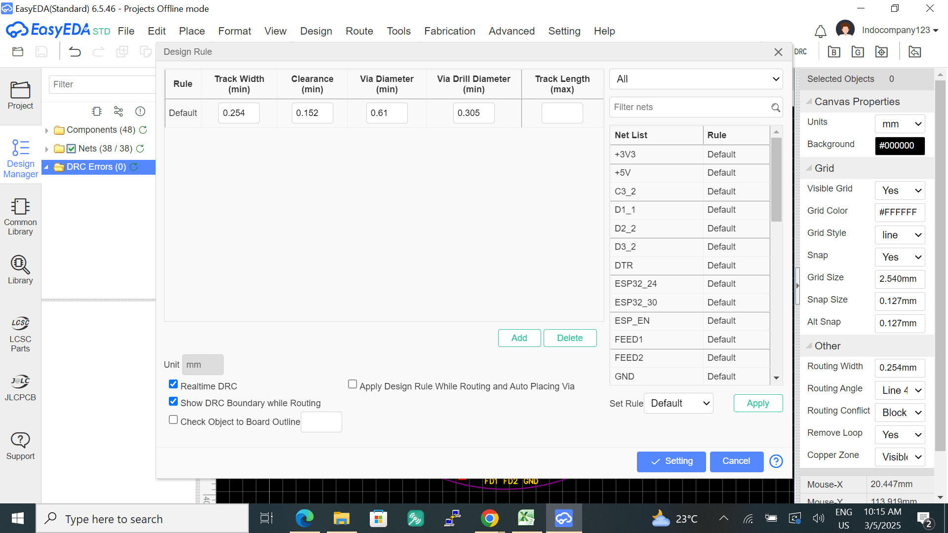
Schematic Design & DRC Verification
-> Designed a schematic with proper power distribution.
-> Verified connections using DRC to prevent floating pins or errors.
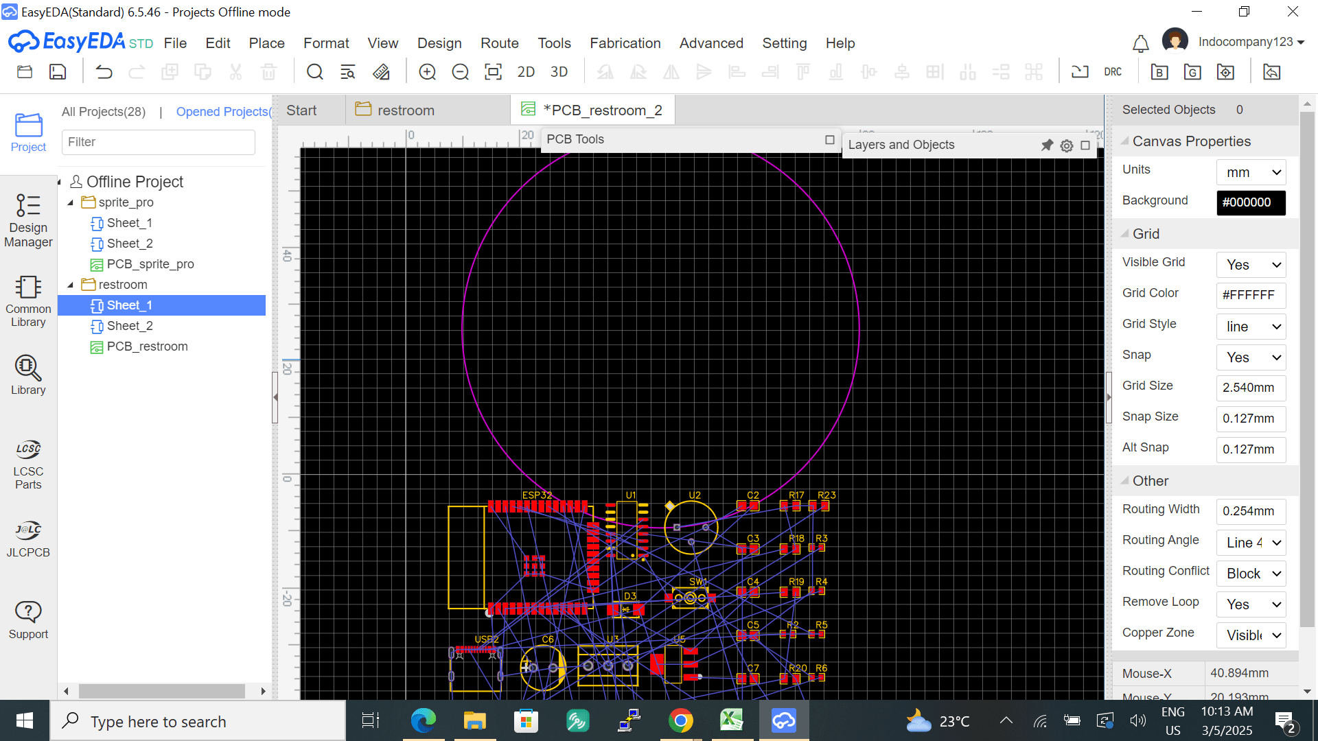
PCB Layout Design & Routing
-> Optimized layout for high-power handling and low-noise operation.
-> Kept power and ground traces close together to reduce electromagnetic interference (EMI).
Difficulties Encountered in PCB Design
Several challenges arise during PCB design, including library management issues, where finding or creating custom symbols and footprints can be time-consuming. Component placement constraints can make routing difficult, especially in compact designs. Signal integrity concerns, such as crosstalk and EMI, require careful layout planning. Thermal management issues must be addressed, particularly in high-power circuits, to prevent overheating. Lastly, design rule violations and manufacturing tolerances must be considered to ensure a successful PCB fabrication.