Introduction to PCB Production
Printed Circuit Boards (PCBs) are the foundation of modern electronic systems, providing both mechanical support and electrical interconnections between electronic components. Almost every electronic device, from simple embedded systems to advanced industrial equipment, relies on PCBs for reliable operation.
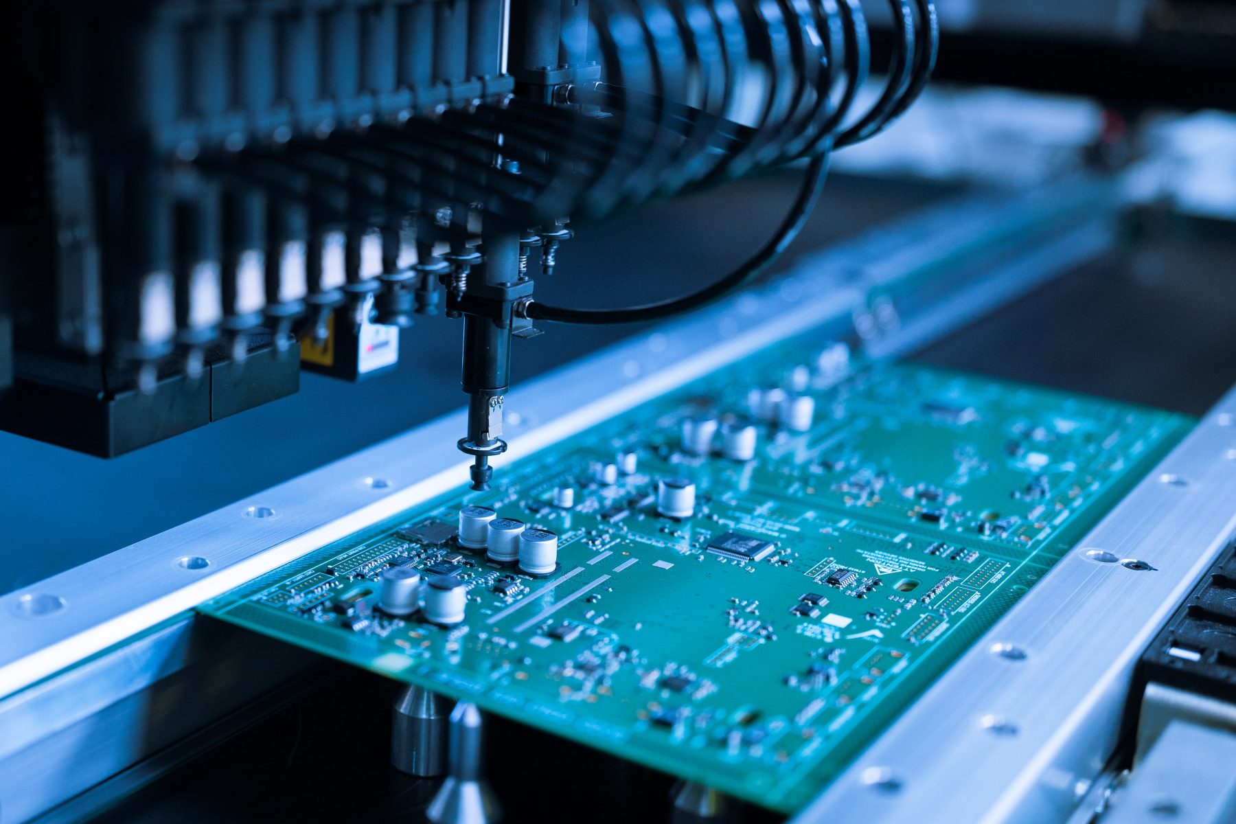
PCB production involves several stages including circuit design, material selection, fabrication, component assembly, inspection, and testing. Depending on the application, PCBs can be manufactured using industrial fabrication processes or produced locally using CNC milling machines for rapid prototyping.
In this group assignment, our objective was to understand the complete PCB production workflow and characterize the capabilities of our in-house PCB fabrication process using the Wegstr PCB Milling Machine. Through a series of tests and observations, we evaluated the design limitations, tooling requirements, machine settings, and manufacturing constraints that influence PCB production.
The knowledge gained from this characterization process helps establish reliable design guidelines for future PCB development and ensures successful fabrication using the available laboratory equipment.
PCB Production Workflow
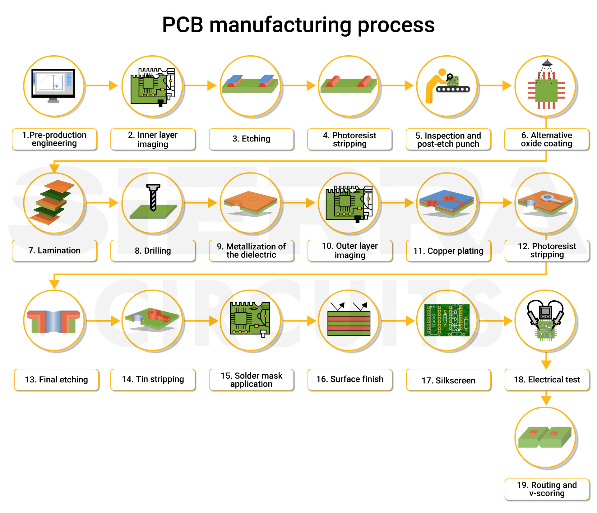
PCB manufacturing follows a structured workflow that transforms a digital circuit design into a functional electronic board. Each stage plays an important role in ensuring the final PCB meets both electrical and mechanical requirements. From design preparation to final testing, every step contributes to the reliability and performance of the finished product.
The workflow begins with PCB design creation, where the schematic and board layout are developed using Electronic Design Automation (EDA) software. Once the design is verified, manufacturing files are generated and prepared for fabrication. The PCB is then produced using either in-house milling techniques or industrial manufacturing processes. After fabrication, electronic components are assembled onto the board, followed by inspection and functional testing to validate the design.
Main Stages of PCB Production
Understanding this workflow helps establish a systematic approach to PCB development and ensures that each stage is completed efficiently and accurately.
Types of Printed Circuit Boards
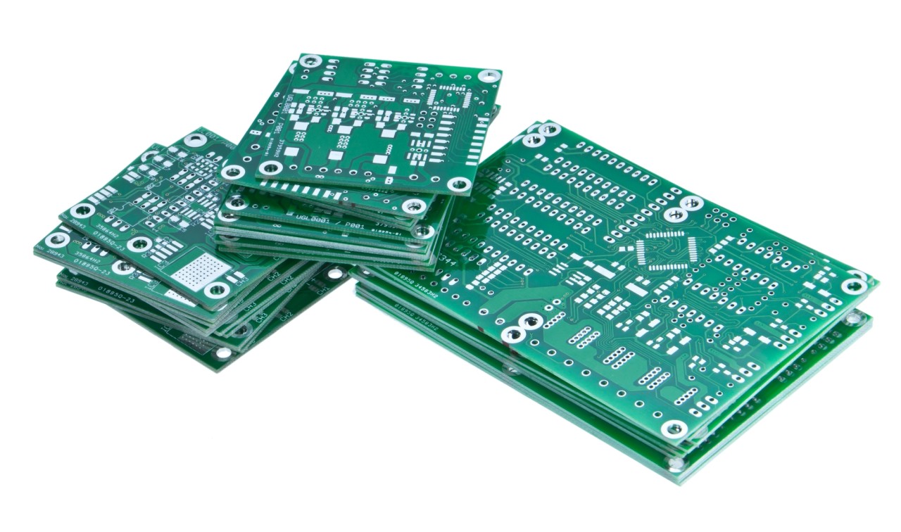
Printed Circuit Boards (PCBs) are available in different configurations depending on the complexity, size, and requirements of the electronic system. The choice of PCB type affects manufacturing cost, circuit density, mechanical flexibility, and overall performance. Understanding these PCB types helps designers select the most suitable fabrication method for their applications.
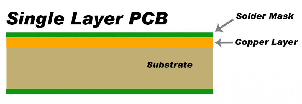
1. Single-Sided PCB
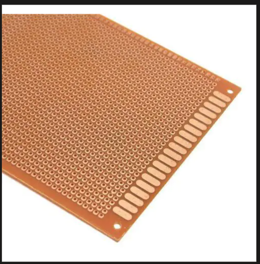
A single-sided PCB contains a conductive copper layer on only one side of the substrate material. Components are mounted on the opposite side, making it the simplest and most economical PCB type. These boards are commonly used in basic electronic circuits, educational projects, and low-complexity embedded systems.
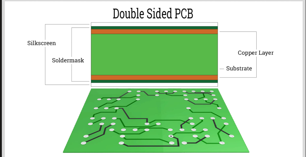
2. Double-Sided PCB
Double-sided PCBs have copper layers on both sides of the substrate, allowing traces to be routed on the top and bottom surfaces. Electrical connections between layers are established using vias. This design provides greater routing flexibility and supports more complex circuits compared to single-sided boards.
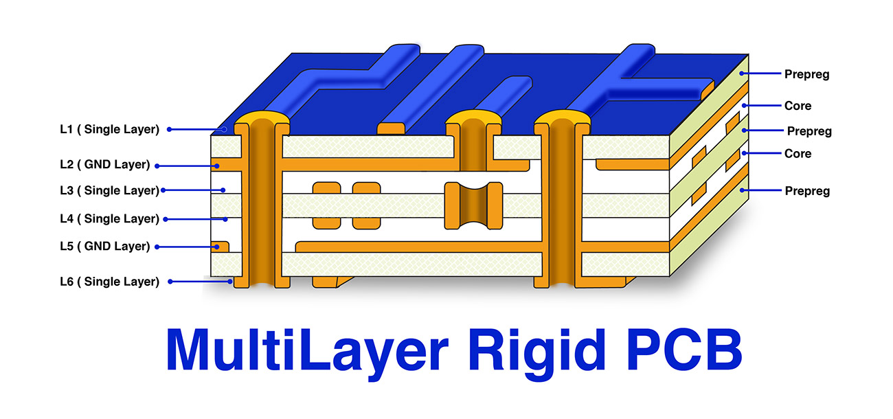
3. Multilayer PCB
Multilayer PCBs consist of multiple conductive layers separated by insulating materials and laminated together. These boards enable high-density circuit designs and are widely used in computers, communication devices, industrial electronics, and advanced embedded systems where compactness and performance are critical.
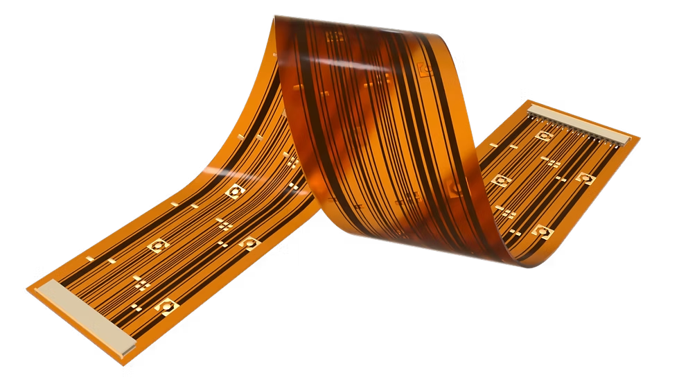
4. Flexible PCB
Flexible PCBs are manufactured using bendable substrate materials that allow the board to flex without damaging the circuit. They are commonly found in wearable electronics, medical devices, cameras, and applications where space constraints or repeated movement are present.
For Fab Academy PCB prototyping, single-sided PCBs are most commonly used because they can be easily fabricated using the Wegstr PCB milling machine. Their simple structure makes them ideal for rapid prototyping and testing of embedded systems and electronic circuits.
PCB Substrate Materials
The substrate material forms the foundation of a Printed Circuit Board and provides both mechanical support and electrical insulation for the copper traces. Different substrate materials offer varying properties such as strength, heat resistance, electrical performance, and manufacturing cost. Selecting the appropriate material is essential for achieving reliable PCB performance.
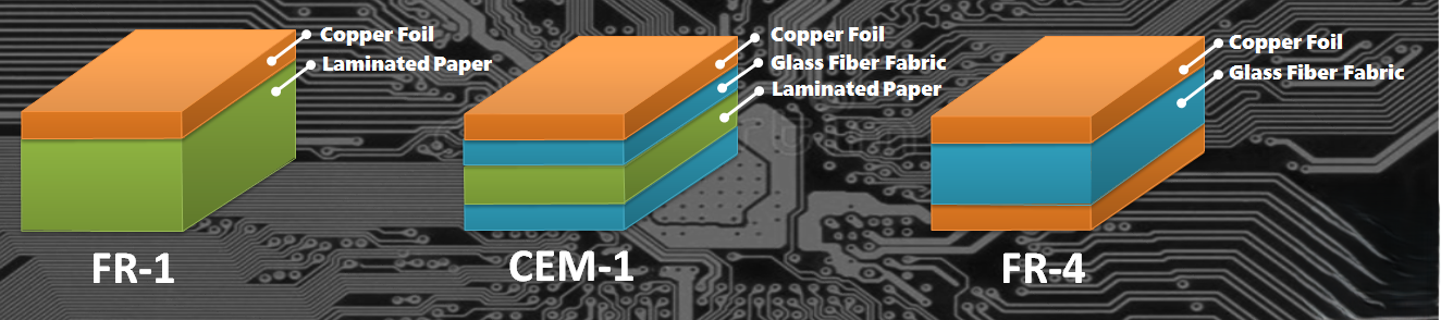
1. FR1
FR1 is a paper-based phenolic laminate commonly used for PCB milling applications in Fab Labs and educational environments. It is easy to machine, produces less tool wear, and generates minimal fiberglass dust during milling. Due to these advantages, FR1 is widely preferred for rapid PCB prototyping using CNC milling machines.
2. FR2
FR2 is another paper-based laminate material that offers low manufacturing costs and is commonly found in consumer electronics. Although suitable for simple circuits, it has lower mechanical strength and thermal resistance compared to modern PCB materials.
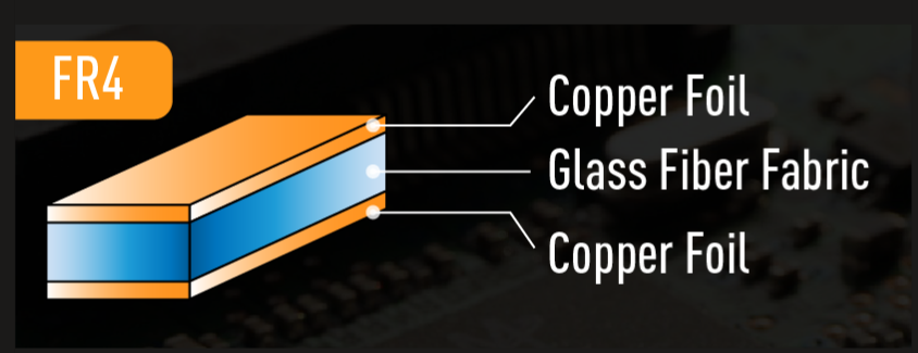
3. FR4
FR4 is the most widely used PCB substrate in the electronics industry. It consists of woven fiberglass reinforced with epoxy resin, providing excellent mechanical strength, thermal stability, and electrical insulation. FR4 is commonly used for commercial and industrial PCB manufacturing.
4. CEM-1
CEM-1 is a composite PCB material that combines paper and fiberglass layers. It offers better strength than FR1 while maintaining relatively low manufacturing costs. CEM-1 is often used in single-sided PCB applications requiring improved durability.
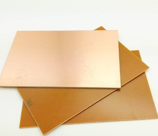
Material Used in Our Lab
For our in-house PCB fabrication process, we used FR1 copper-clad boards. FR1 is particularly suitable for CNC milling because it is easy to machine, produces cleaner cuts, and reduces wear on milling tools. Its properties make it an ideal choice for rapid prototyping and design-rule characterization using the Wegstr PCB milling machine.
PCB Production Process Flow
PCB production involves a series of interconnected steps that transform a digital circuit design into a fully functional electronic board. Each stage contributes to the overall quality, reliability, and manufacturability of the final PCB. Understanding this workflow is essential for successful in-house PCB fabrication and helps identify potential issues before production.
For this characterization exercise, we followed a complete PCB fabrication workflow beginning with circuit design and ending with assembly and testing. The workflow ensured repeatability and allowed us to evaluate the capabilities and limitations of our in-house PCB production process.
PCB Milling Tools
The quality and accuracy of PCB fabrication depend heavily on the selection of appropriate milling tools. Different tools are used for trace isolation, drilling, and board profiling. During the characterization process, we studied the various milling bits used in the Wegstr PCB milling machine and their influence on machining quality and dimensional accuracy.
Common PCB Milling Tools
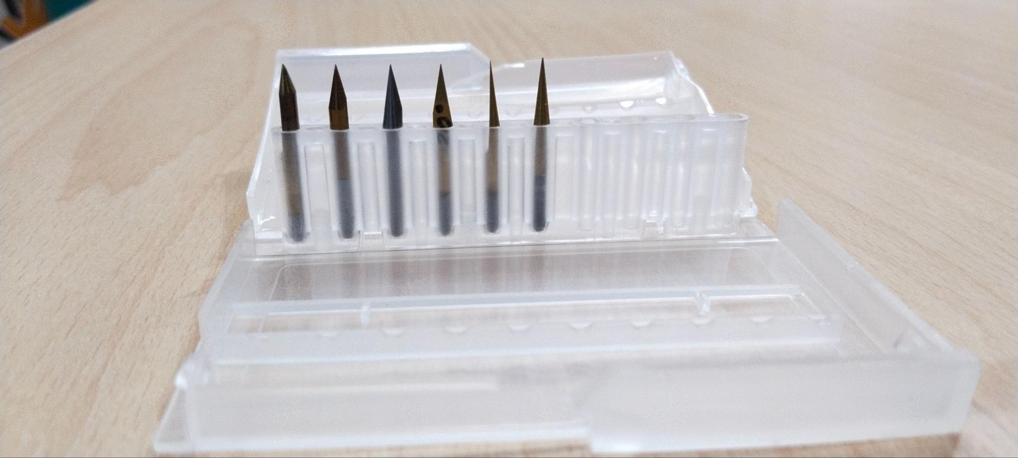
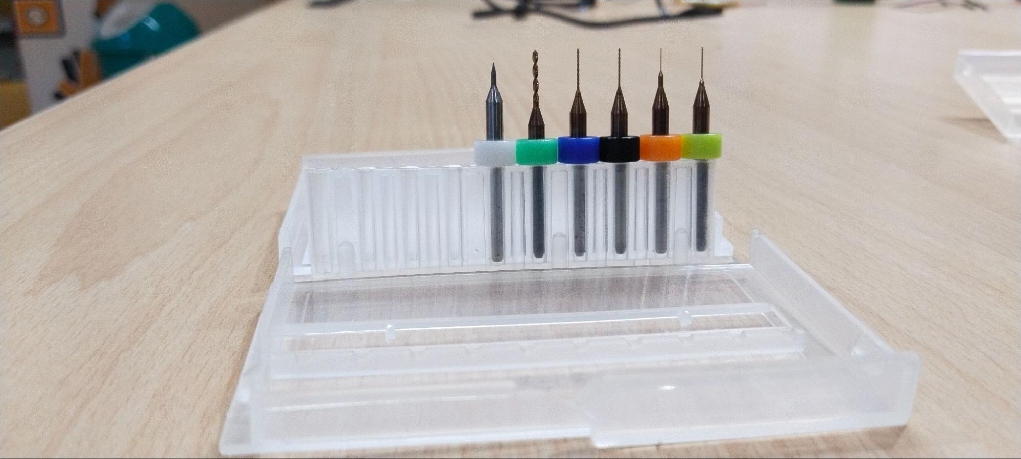
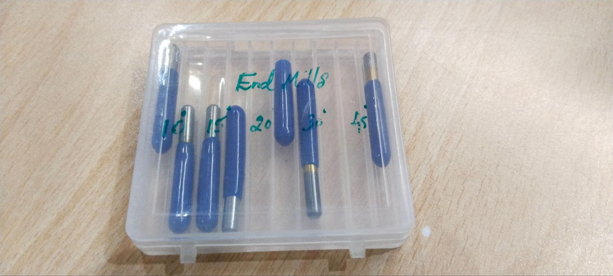
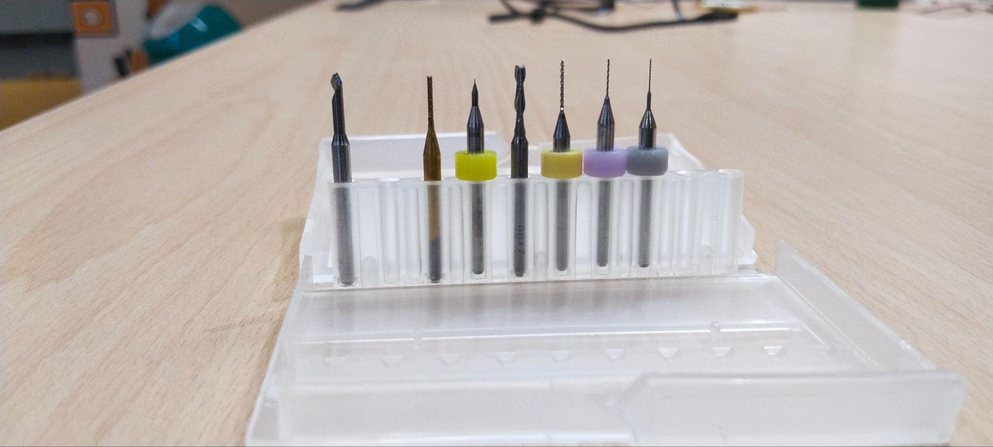
| Tool | Diameter | Purpose |
|---|---|---|
| V-Bit | 0.1 mm Tip | Trace Isolation Milling |
| Drill Bit | 0.8 mm | Drilling Component Holes |
| Drill Bit | 1.0 mm | Larger Mounting Holes |
| End Mill | 2.0 mm | PCB Outline Cutting |
Wegstr PCB Milling Machine
The Wegstr PCB Milling Machine is a compact desktop CNC system specifically developed for rapid PCB prototyping and small-scale electronics manufacturing. Unlike traditional PCB fabrication methods that rely on chemical etching, the Wegstr machine mechanically removes unwanted copper from a copper-clad board using precision milling tools. This approach enables fast design iteration, reduced chemical waste, and immediate verification of electronic designs within a laboratory environment.
The machine is capable of producing PCB traces, drilling holes, and cutting board outlines with high accuracy. Combined with CAM software and auto-levelling capabilities, it provides an efficient workflow for transforming digital PCB designs into physical prototypes.
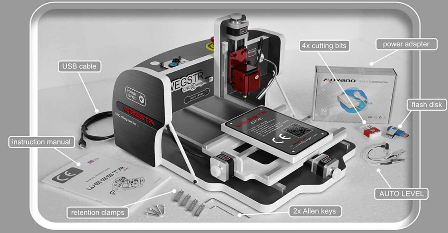
The Wegstr system is particularly suitable for educational environments, research laboratories, Fab Labs, and rapid prototyping applications where quick turnaround and iterative development are important.
Key Features of the Wegstr PCB Milling Machine
Machine Specifications
Understanding the machine specifications is important when characterizing the PCB production process. The machine's working area, spindle speed, tool compatibility, and positioning accuracy directly influence the quality and repeatability of PCB fabrication.
| Parameter | Specification |
|---|---|
| Machine Name | Wegstr PCB Milling Machine |
| Machine Type | Desktop CNC PCB Milling Machine |
| Working Area | 140 mm × 200 mm |
| Spindle Speed | Up to 11,000 RPM |
| Supported Operations | PCB Trace Milling, Drilling, Board Profiling |
| Communication Interface | USB |
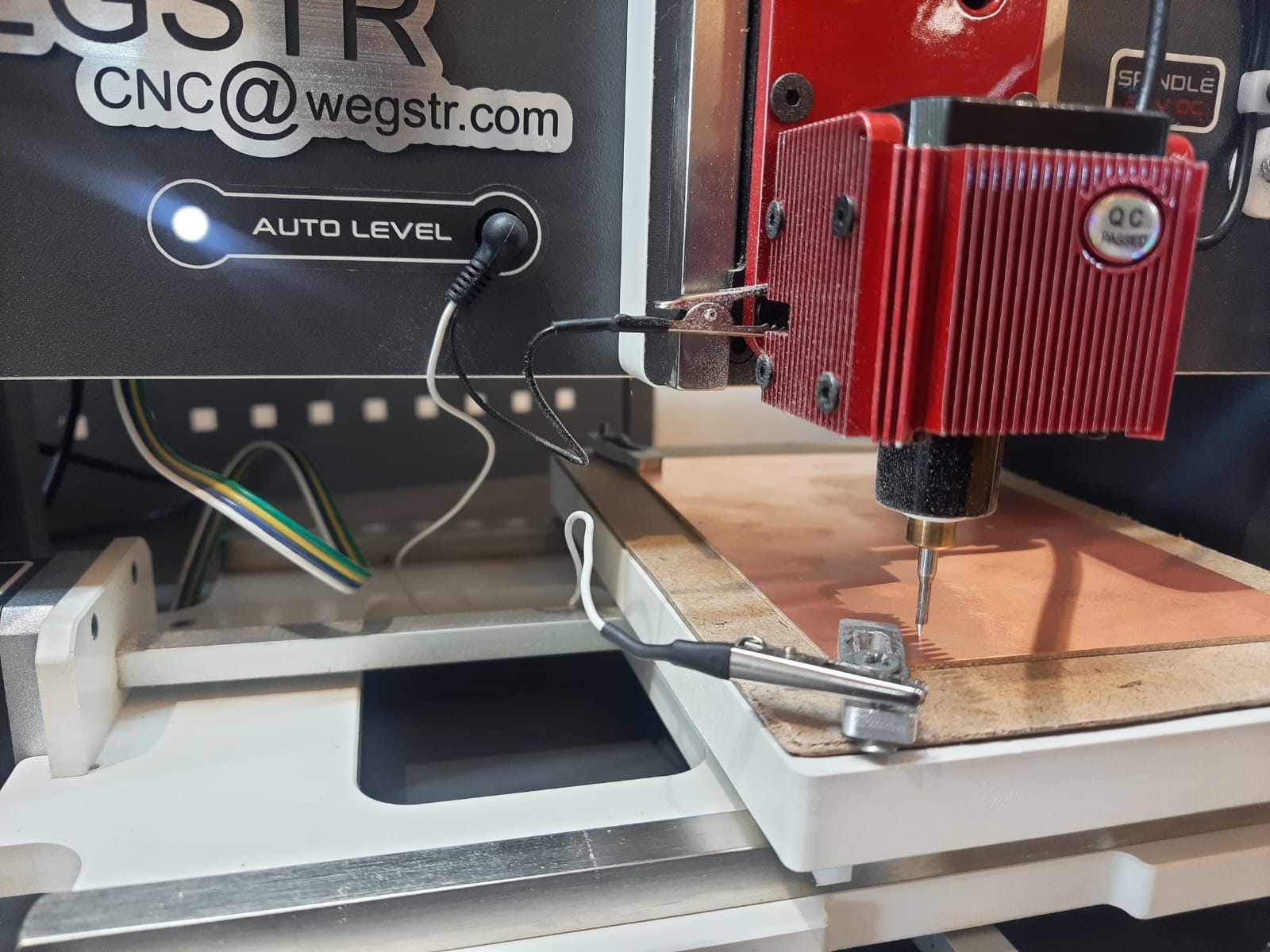
| Auto Levelling | Supported |
| Control Software | Wegstr Controller Software |
| Toolpath Software | MODS CE |
| PCB Material | FR1 Copper Clad Board |
These specifications make the Wegstr machine suitable for rapid PCB prototyping, allowing users to fabricate and test electronic circuits without relying on external PCB manufacturing services.
Machine Setup Procedure
Before starting the PCB milling process, the Wegstr PCB milling machine must be properly configured and connected to the control software. Correct machine setup ensures reliable communication, accurate positioning, and safe operation during fabrication. The following procedure was followed to prepare the machine for PCB milling.
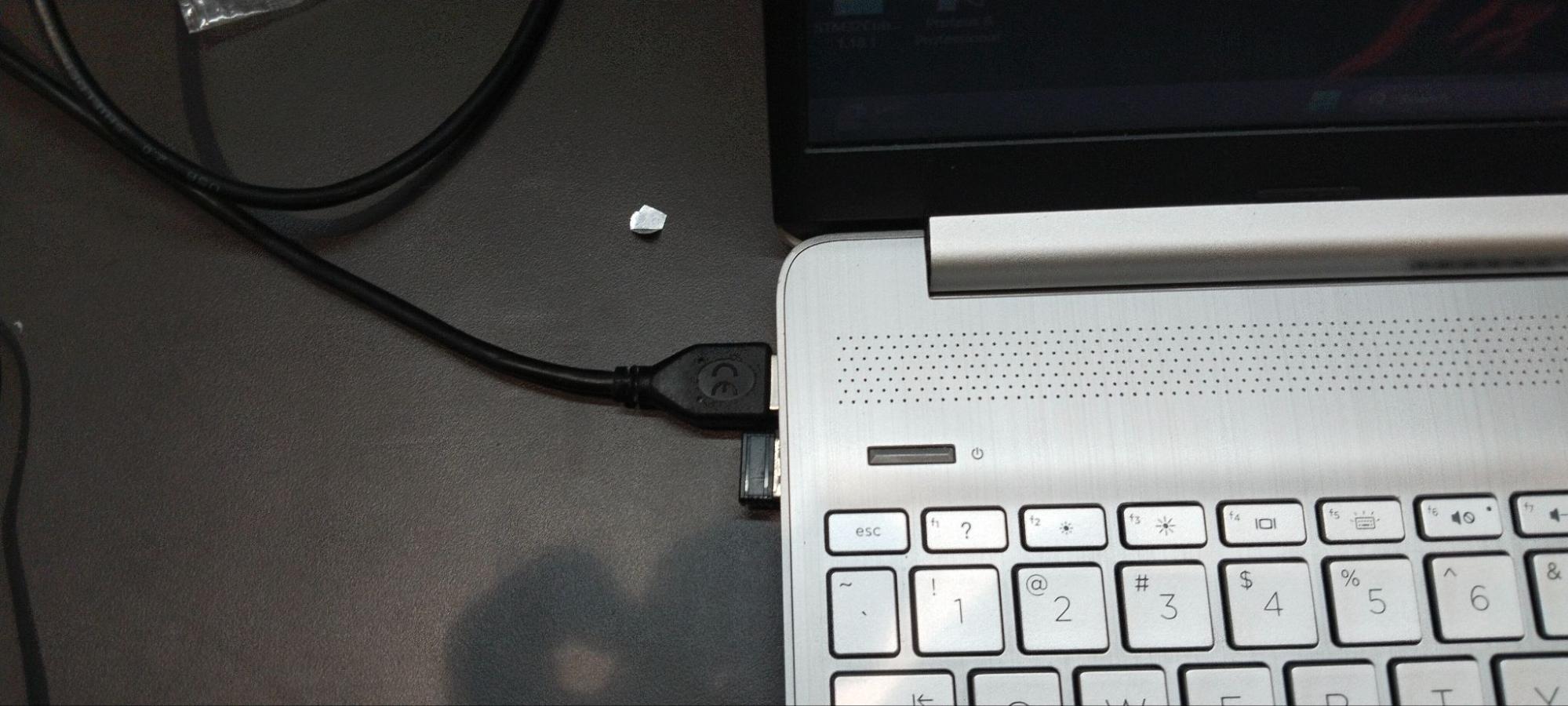
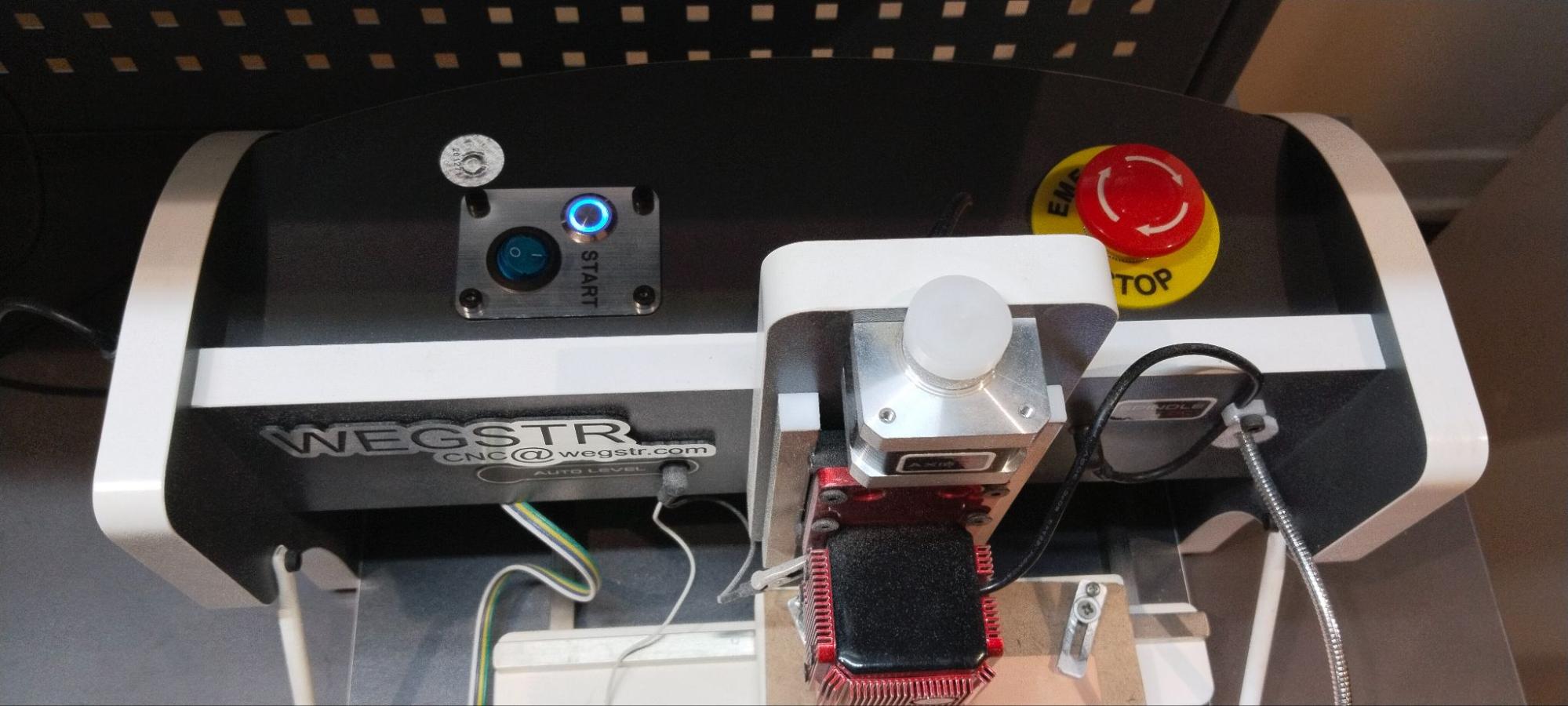
Step 1 – Connect the Machine via USB
The Wegstr PCB milling machine was connected to the computer using a USB cable. This connection enables communication between the machine controller and the control software, allowing toolpaths and commands to be transmitted directly to the machine.
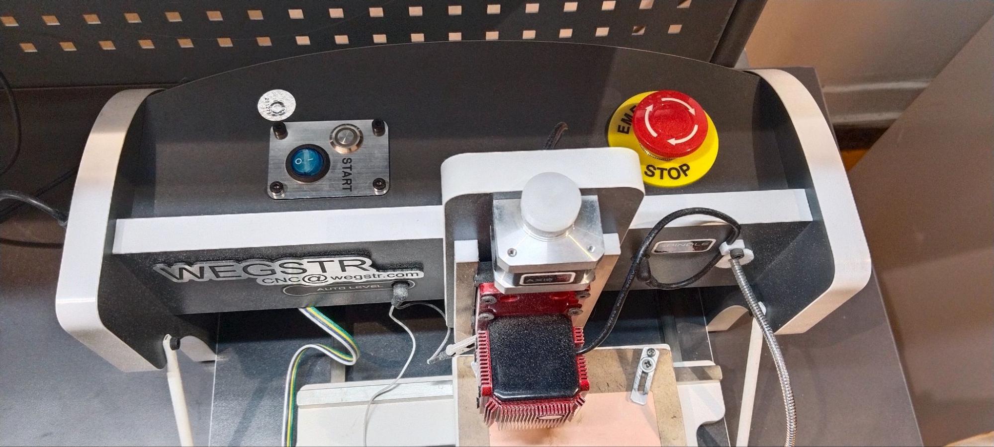
Step 2 – Power On the Machine
After establishing the USB connection, the machine was powered on using the main power switch. During startup, the machine initializes its internal systems and prepares for communication with the control software.
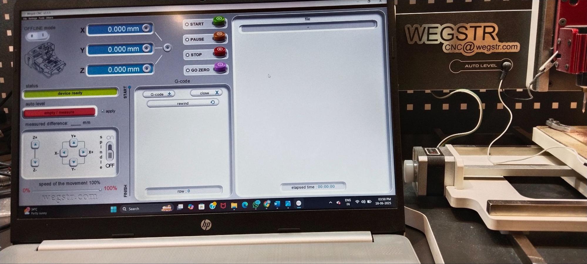
Step 3 – Launch the Wegstr Control Software
The Wegstr control software was opened on the computer. Once launched, the software automatically searched for connected devices and established communication with the PCB milling machine.
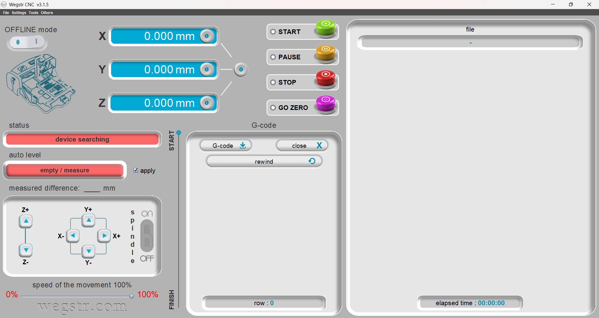
Step 4 – Verify Device Connection
After successful communication was established, the machine status was displayed within the software interface. A blinking indicator LED on the machine confirmed that communication between the computer and the machine was active.
Step 5 – Test Machine Movement
The X, Y, and Z axes were manually jogged using the software controls to verify proper machine operation. This step ensured that all axes responded correctly before loading the milling files.
Once communication and motion testing were completed successfully, the machine was ready for PCB preparation, toolpath loading, and milling operations.
Preparing PCB Files and Generating Toolpaths Using MODS CE
After completing the PCB design in KiCad, the next step was to generate machine-readable toolpaths for fabrication. Since the Wegstr PCB milling machine cannot directly interpret PCB design files, the design must first be converted into CNC toolpaths using CAM software. For this workflow, we used MODS CE (Community Edition), a browser-based digital fabrication platform developed by MIT's Center for Bits and Atoms.
MODS CE allows users to convert PCB design files into NC (Numerical Control) files that can be executed by the milling machine. The software calculates the required toolpaths, offsets, cutting depths, and isolation routes needed to fabricate the PCB accurately.
Step 1 – Export the Front Copper Layer
Once the PCB layout was finalized in KiCad, the front copper layer (F.Cu) was exported as an SVG file. This layer contains all copper traces, pads, and electrical connections that will be milled onto the PCB surface.
Step 2 – Export the Edge Cut Layer
The board outline was exported separately as an SVG file from the Edge Cuts layer. This file defines the physical dimensions and shape of the PCB and is used during the final profiling operation.
Step 3 – Open MODS CE
The MODS CE web interface was opened and the PCB milling workflow was selected. This environment provides tools for importing design files, configuring machining parameters, and generating CNC toolpaths.
Step 4 – Generate Trace Milling Toolpaths
The front copper SVG file was imported into MODS CE. For trace isolation milling, a 0.1 mm 20° V-Bit was selected. Appropriate offsets were applied to ensure complete copper isolation between adjacent traces. MODS then calculated the required milling paths and generated the corresponding NC file.
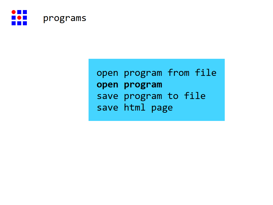
Figure 1: Opening the MODS CE program menu to select the appropriate PCB milling workflow.
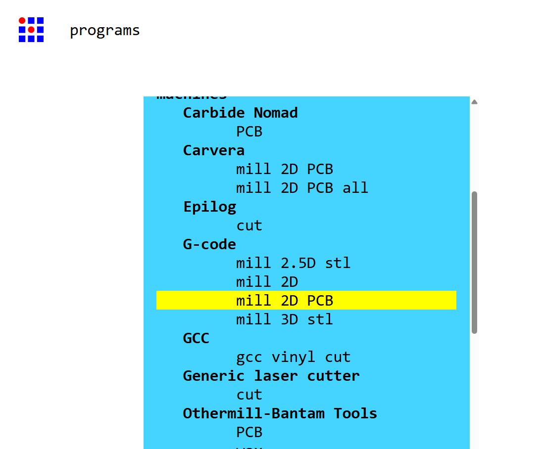
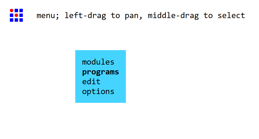
Figure 2: Selecting the "Mill 2D PCB" program from the available machining workflows in MODS CE.
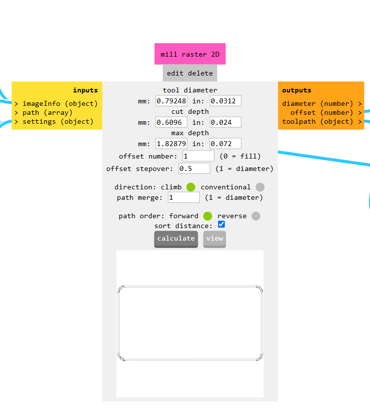
Figure 3: Importing the exported SVG file into MODS CE for toolpath generation.
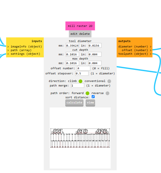
Figure 4: Configuring the default PCB milling parameters including tool diameter, cut depth, offsets, and spindle feed settings.
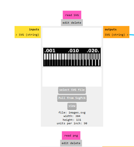
Figure 5: Setting the trace isolation milling parameters using a 1/64-inch milling tool for engraving PCB traces.
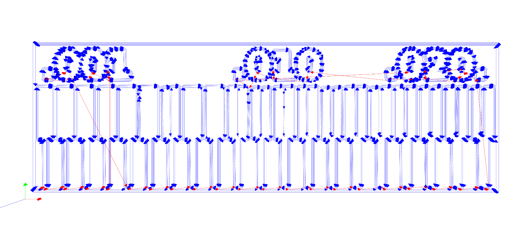
Figure 6: Configuring the board outline cutting parameters using a 1/32-inch end mill for PCB profiling.
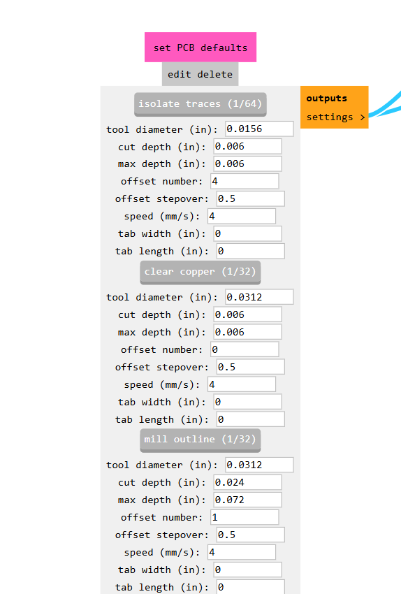
Figure 7: Preview of the generated CNC toolpath showing the isolation routes that will be followed during PCB milling.
Step 5 – Generate Board Outline Toolpaths
The Edge Cuts SVG file was imported separately into MODS CE. For board profiling operations, an end mill was selected to cut the PCB outline. After verifying the cutting parameters, the NC file for the board outline was generated.
Step 6 – Download NC Files
After the calculations were completed, MODS CE generated separate NC files for trace milling and board outline cutting. These files were then imported into the Wegstr control software and used for the PCB fabrication process.
This workflow ensures that the PCB design is accurately translated into machine instructions while maintaining the required trace widths, clearances, and board dimensions.
Machine Characterization and Design Rules
Before fabricating actual circuit boards, it is important to characterize the PCB milling machine and determine its manufacturing limits. Machine characterization helps identify the minimum trace width, isolation distance, and feature size that can be reliably produced. This information is essential when designing PCBs because it ensures that the generated layouts can be successfully fabricated without broken traces or short circuits.
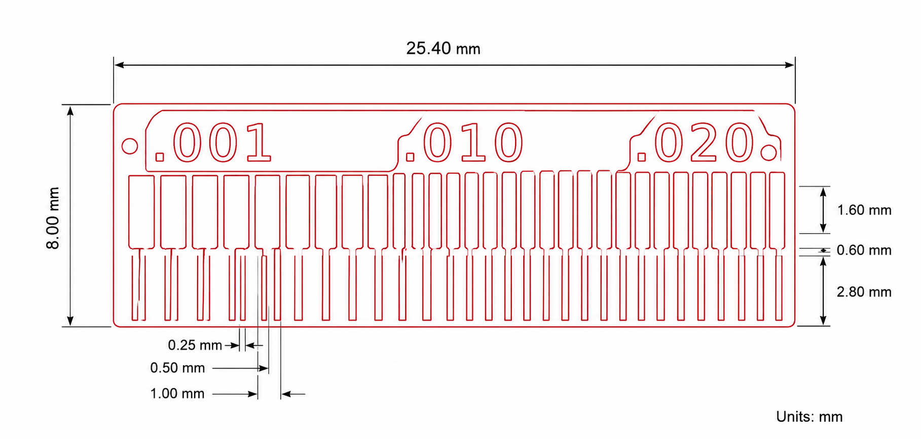
To characterize our in-house PCB production process, we milled a PCB test pattern containing traces and clearances of different widths. The test pattern included features ranging from 0.001 inch to 0.020 inch, allowing us to evaluate the machine's milling accuracy and determine the smallest manufacturable feature.
Test Procedure
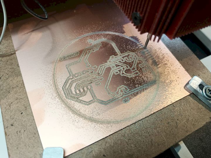
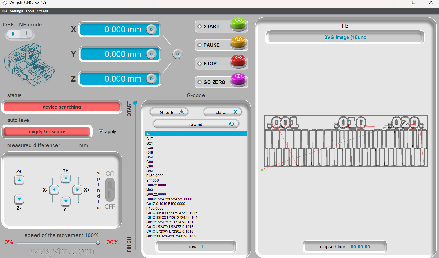
After generating the NC file from the previously prepared toolpath, the file was loaded into the Wegstr PCB milling machine software. A 1/64-inch milling bit was installed, and the machine origin was set using the standard setup procedure. The test pattern was then milled onto a copper-clad board under normal operating conditions.
Once the milling process was completed, the fabricated test board was inspected visually to evaluate the isolation quality between traces. The resulting pattern was analyzed to identify the minimum trace width and clearance that could be reliably produced using our in-house PCB milling process.
PCB Milling Output
After generating the NC file and loading it into the Wegstr PCB milling machine, the characterization pattern was fabricated on an FR1 copper-clad board using a 1/64-inch milling bit. The resulting PCB was inspected to evaluate trace isolation, machining accuracy, and the minimum manufacturable feature size. The test pattern helped establish the practical design rules for our in-house PCB production process by identifying the smallest trace widths and clearances that could be reliably milled.
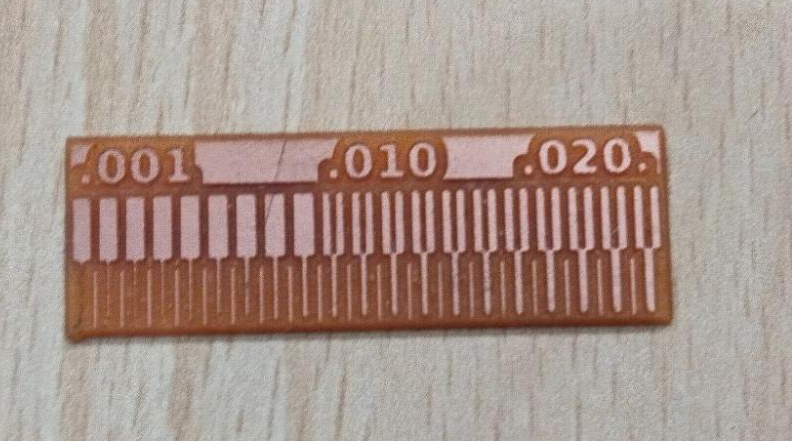
The fabricated board demonstrated successful isolation of larger traces and clearances while highlighting the limitations of extremely fine features. Based on these observations, the machine characterization results were used to define the recommended design rules for future PCB fabrication using the Wegstr milling machine.
Observed Results
| Feature Size | Result |
|---|---|
| 0.001 inch | Not Successfully Milled |
| 0.010 inch | Partially Visible |
| 0.020 inch | Successfully Milled |
Based on the characterization results, the machine was able to reliably produce traces and clearances around 0.020 inch under the selected milling conditions. Features smaller than this became increasingly difficult to fabricate consistently due to tool diameter limitations and machine tolerances.
Design Rules Established
- Minimum trace width: 0.020 inch
- Minimum isolation clearance: 0.020 inch
- Trace milling tool: 1/64 inch V-Bit
- Outline milling tool: 1/32 inch End Mill
- PCB Material: FR1 Copper Clad Board
These design rules were used throughout subsequent PCB design activities to ensure reliable manufacturing and repeatable fabrication results.
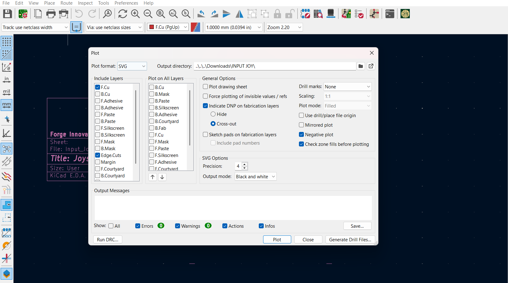
Preparing PCB Files for Board House Fabrication
As part of the Electronics Production group assignment, the PCB design was prepared for external fabrication by generating Gerber and drill files from KiCad. Gerber files contain all the manufacturing information required by PCB manufacturers, including copper layers, board outlines, solder mask information, and drill locations.
Before generating the manufacturing files, the PCB design was verified and finalized in KiCad PCB Editor. The board outline, copper traces, and component footprints were checked to ensure that the design was ready for fabrication.
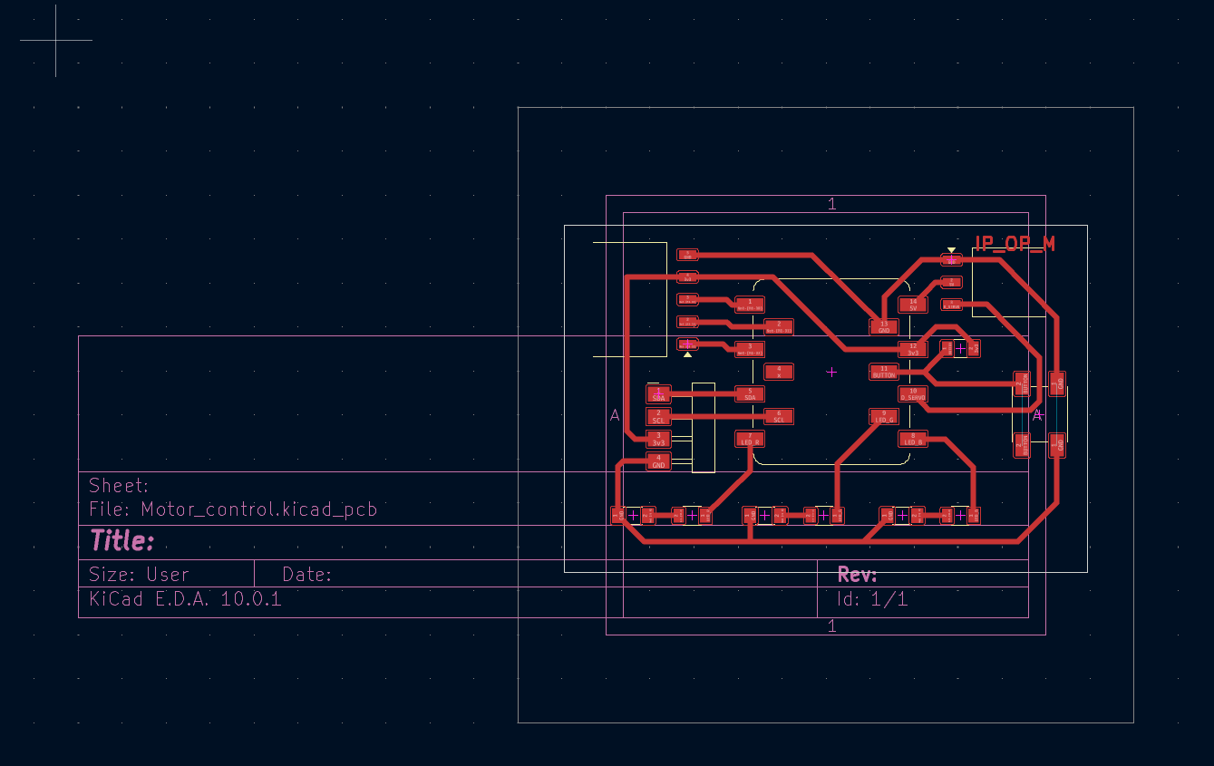
The Plot tool was opened from the PCB Editor and the output format was set to Gerber. The required manufacturing layers were selected, including the top copper layer (F.Cu) and board outline layer (Edge.Cuts). The Gerber job file option was enabled and the selected layers were plotted to generate the fabrication files.
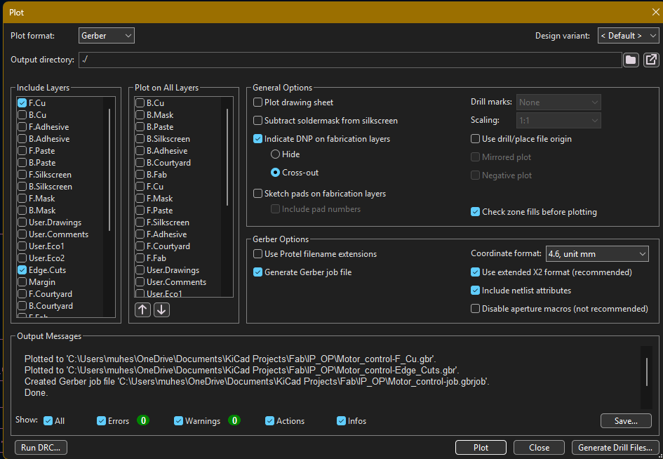
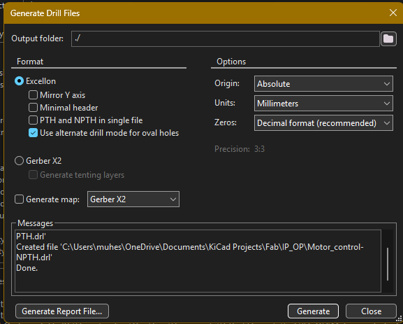
After generating the Gerber files, the drill file generation tool was opened. Drill files contain the hole information required for PCB manufacturing. The Excellon format was selected with millimeter units, and the drill file was generated successfully.
Once the Gerber and drill files were generated, all manufacturing files were collected and compressed into a ZIP archive. This ZIP package is the standard format accepted by most PCB fabrication services.
Uploading Gerber Files to JLCPCB
To verify the manufacturability of the design, the generated Gerber ZIP file was uploaded to the JLCPCB online quotation platform. After uploading, the system automatically analyzed the files and generated a PCB preview along with fabrication parameters.
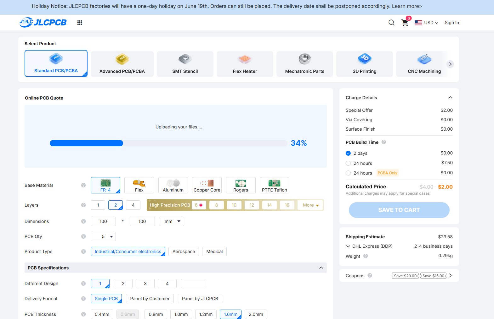
The uploaded PCB design was successfully recognized by the JLCPCB system. The board dimensions, layer information, and manufacturing parameters were automatically extracted from the Gerber files.
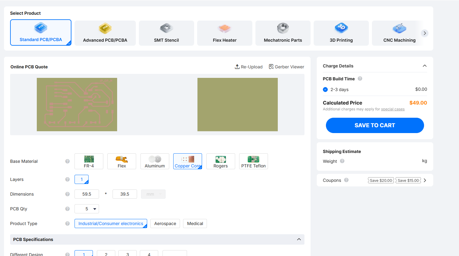
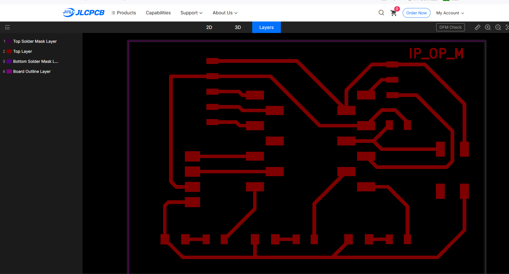
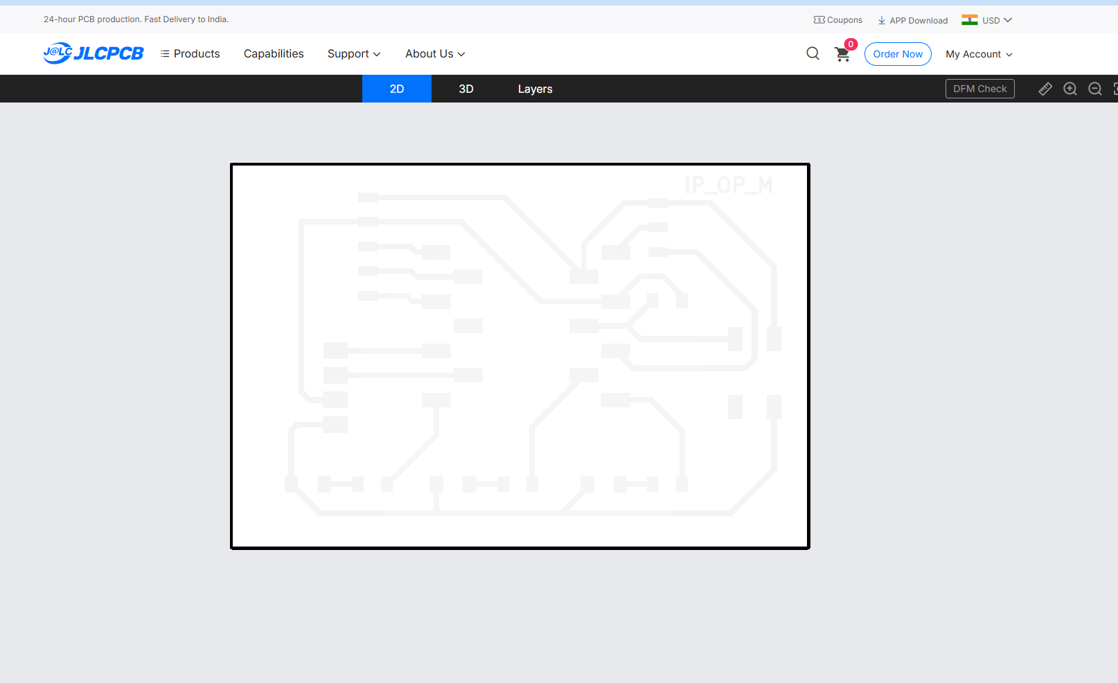
The Gerber Viewer provided by JLCPCB was then used to inspect the generated manufacturing layers. This verification step ensured that the copper traces, pads, and board outline were correctly exported before proceeding to fabrication.
Learning Summary
This group assignment provided a comprehensive understanding of the complete PCB production workflow, from design preparation to final fabrication. We studied different PCB types, substrate materials, milling tools, and fabrication methods used in modern electronics manufacturing.
Through the characterization of the Wegstr PCB Milling Machine, we learned how machine limitations influence PCB design decisions. By fabricating a trace characterization board, we identified the minimum trace width and isolation clearance that can be reliably produced using our in-house manufacturing process.
We gained practical experience in generating manufacturing files from PCB designs, converting SVG files into machine-readable NC files using MODS CE, and executing milling operations on the Wegstr PCB milling machine. Understanding the relationship between tool diameter, machining parameters, and PCB quality helped us establish reliable fabrication guidelines.
Additionally, we explored the workflow required for professional PCB manufacturing through board houses, including Gerber generation, drill file creation, design verification, and fabrication submission procedures. This helped us understand the differences between rapid in-house prototyping and industrial PCB production.
Overall, this assignment strengthened our knowledge of PCB fabrication processes, manufacturing constraints, machine characterization, and design-for-manufacturing principles that will be applied throughout future electronic design projects.
Downloads
The files generated and used during the PCB production characterization process can be downloaded below.
| S.No | File Name | Description | Download |
|---|---|---|---|
| 1 | Trace Characterization SVG | Test pattern used for machine characterization. | Download SVG |
| 2 | Trace Milling NC File | Generated NC file for trace isolation milling. | Download NC |
| 3 | Gerber Manufacturing Package | Complete fabrication package containing Gerber files, board outline, copper layers, and drill files generated from KiCad for PCB manufacturing. | Download ZIP |