Week 6 : Electronics Design
This week we are learning how to design a development board. We are tasked with using an EDA (Electronic Design Automation) tool to design a PCB board that uses parts from the inventory to interact and communicate with an embedded microcontroller. Also, for our group assignment, we are to use test equipment in the lab to observe the operations of a microcontroller circuit board.
Designing a Development Board with an EDA Tool
- I do want to state, if you have never learned this process before and this is your first time working with any of these tools or processes, this would be very hard to accomplish in the time allotted without more guidance and a tutorial. I could not have accomplished what I have so far without the in-depth hands on assistance provided by Peter and Tom from Moonlighter.
- I will be using KiCad, an open-source program to design my PCB board. Go to the KiCad website and download/ Install KiCad.- In our schedule/assignment page, there is a libraries link is where you can download the libraries that fab academy has made accessible to us. Unzip the files
- Once you install KiCad it will automatically make a folder in your documents folder labeled “KiCad”. Move the unzipped libraries folder into the Kicad folder. Rename the kicad masters library folder as “Fab”.
- Open Kicad. Start a new project under the file tab. Save it in your Kicad folder.
- Then go to preferences. We first want to manage of symbol libraires. Scroll down all the way. Hit the plus button and find where you have the “Fab” folder. Open the Kicad_sym file. And name it kicad.sym.
- The we go back to preferences and we are going to manage the footprint libraires. Hit the plus button and find the “Fab” folder again. Select the “Fab.pretty” folder and open it there.
- For the last thing to set up, got to preferences, then configure paths. For this, you want to get to the same folder but by clicking on the complete path to get to that folder. For example, for me I went to documents folder, then the kicad folder, and then the fab folder(no shortcuts to find the fab folder). Add it in and you’ll gain access to all the models.
- Ideally for my final project I would like my jewelry display stand to have a light and motion feature that is possibly controlled by two input options, a motion sensor and a master switch. So, I will need to design my PCB board to interact with two inputs and two outputs.
- We will start with the schematic. Click on schematic editor and it will open up a new window to work in. Apparently, KiCad loves windows and we will be dealing with a bunch of multiple windows on this KiCad journey.
- To start, click on the symbol editor button which will take you to another window to be able to search the symbol libraries we previously loaded from the Fab Academy. Search for the microcontroller you plan on using. I will be using the XAIO RP2040. For the moment, I plan on using the the socketSMD schematic. There are pros and cons to using a SMD (surface mount device) but for now I think using a SMD is most beneficial.

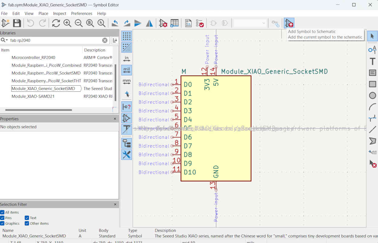
- Select your controller schematic and hit at add symbol to schematic button, which will take you back to your schematic window and add it there.
- We will start adding tags/symbols to help better organize our schematic
- To the right, there is a symbol that looks like a ground symbol and from there you can add different power and ground symbols to you schematic. Now whenever using these symbols anywhere else in your schematic, they will be linked together and have a theoretical connection.
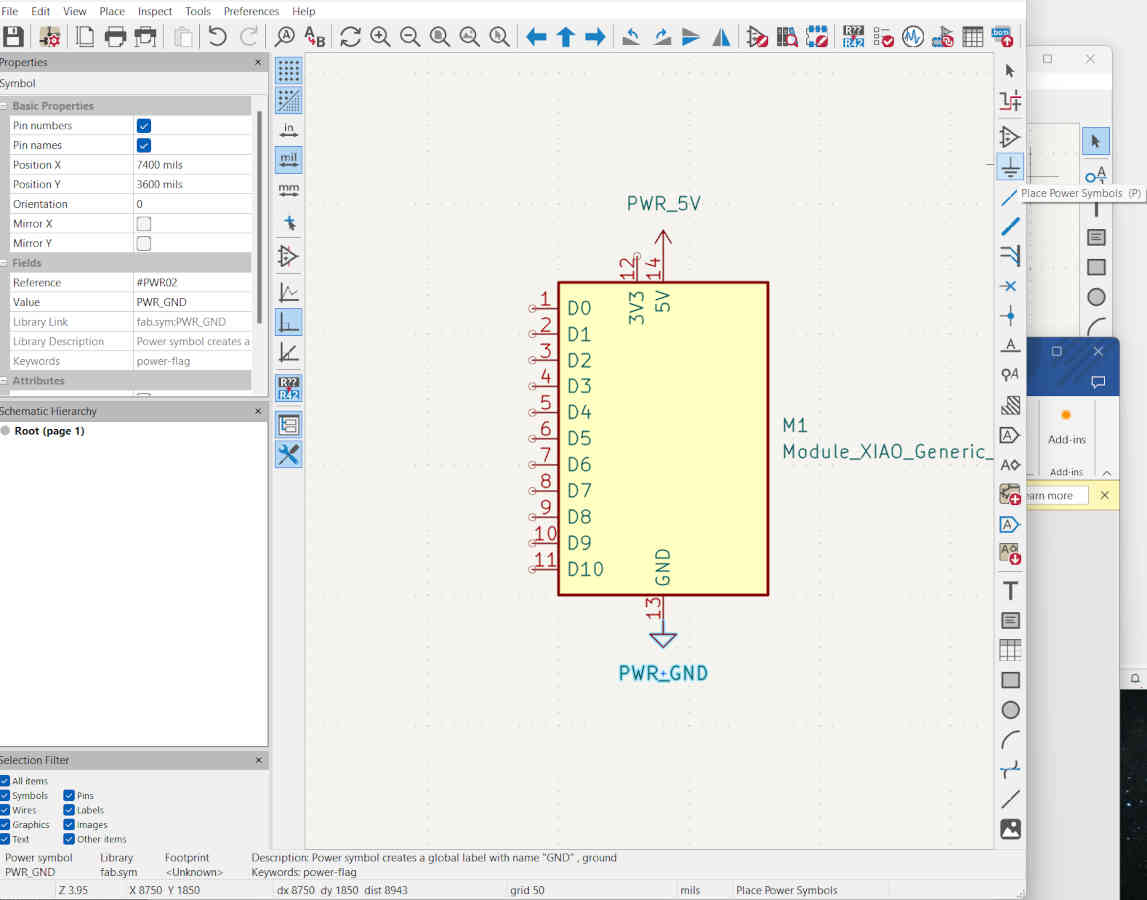
- We will start adding more symbols to build out our board. I will be grabbing a pin header to make testing and attaching my input and output devices easier while allowing for more play area and better flow for shaping what will enclose the finished architecture.
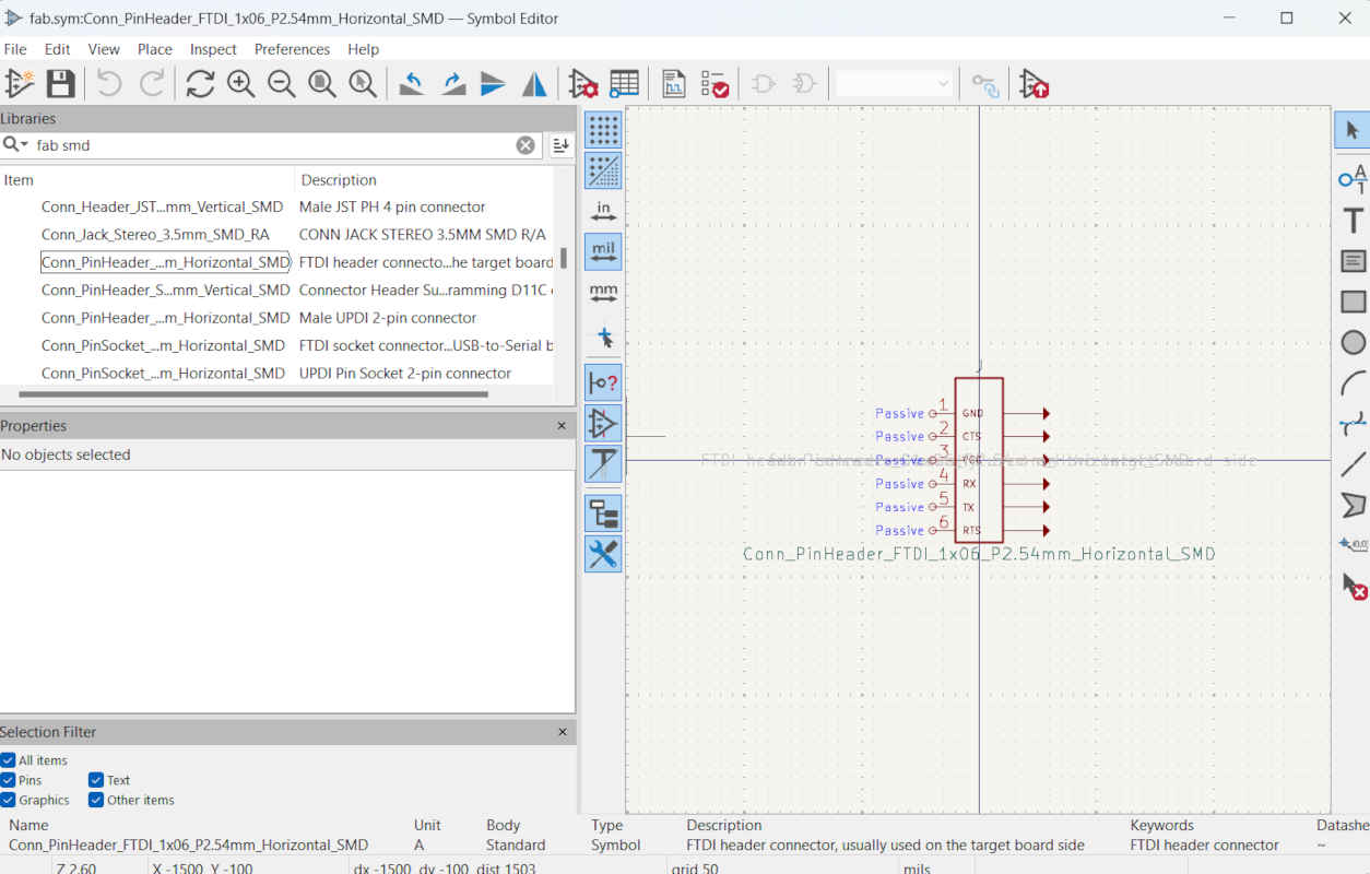
- The schematic was not allowing me to connect my wires to the pinhead I had originally added which threw me off for a bit until I realized it was the incorrect pinhead. I went back and grabbed the correct on to continue.
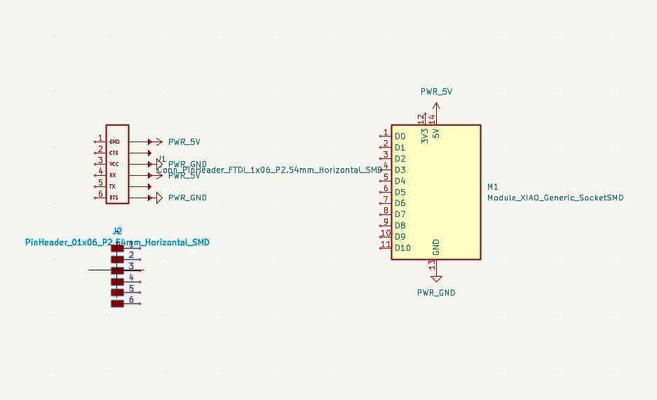
- You want to layout your power, ground, and wires according following the ports/wires of your devices that will be interacting with the microcontroller. Every component needs power and ground. The middle piece/third pin is what sends signal from controller to component and visa versa.
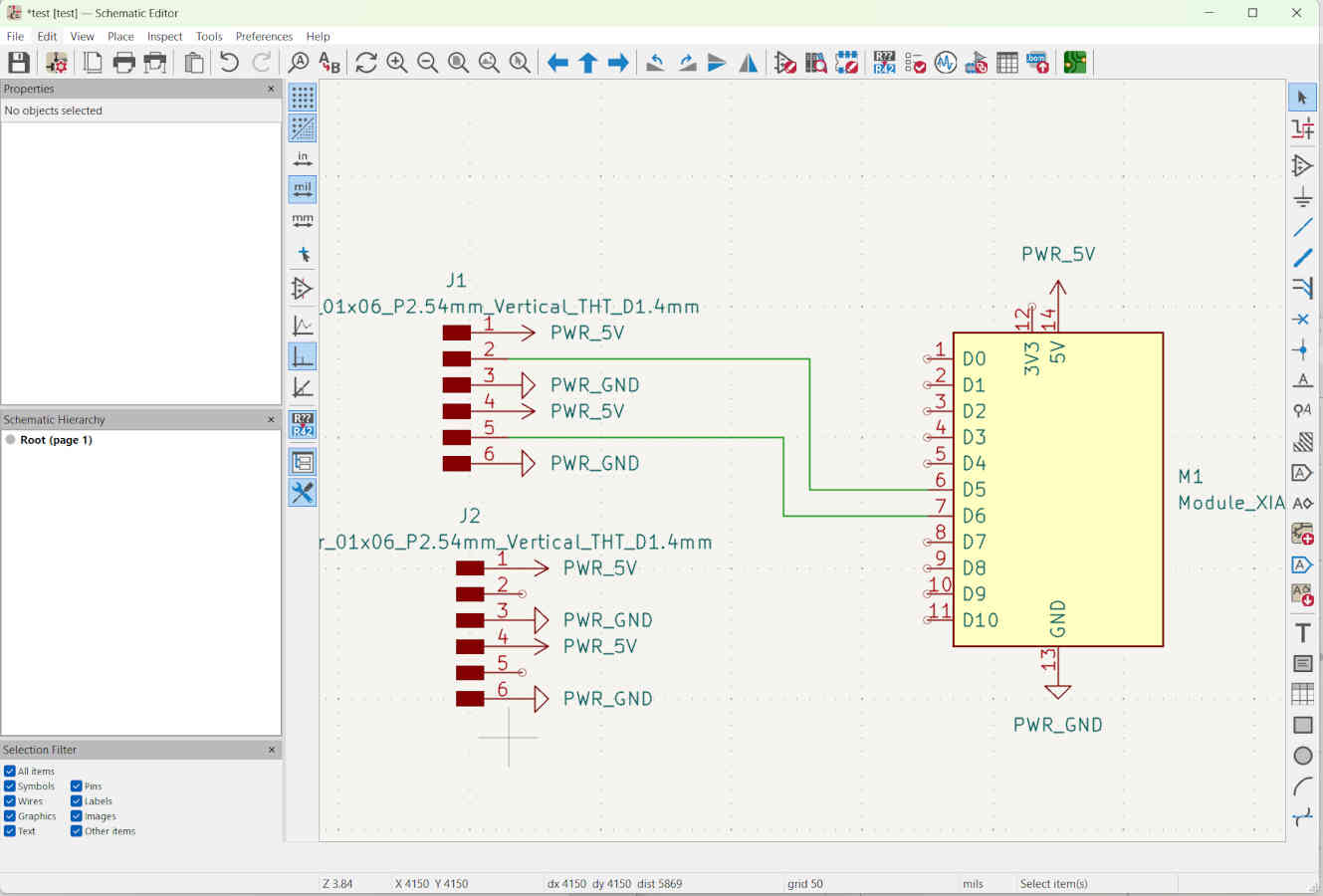
- Don’t forget to check the pin layout of your microcontroller and consider how the physical flow of connections and wires will affect your design and architectural buildout.
- Once you create your layout, you are going to want to place “no connection flags” on the open pins that will not be used to connect to an input or output. They will be a little blue “X”.
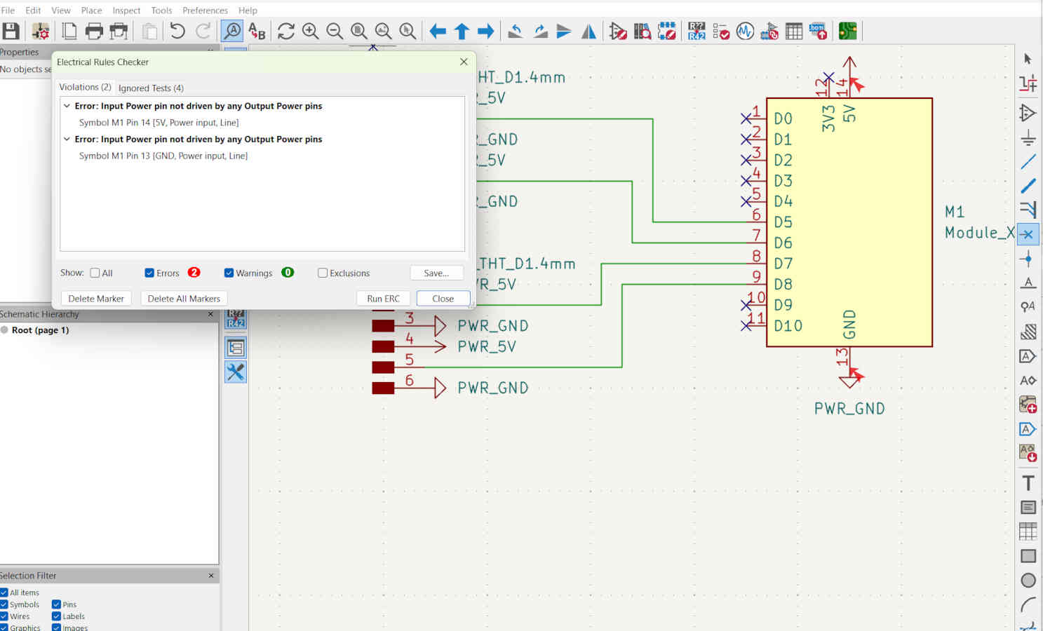
- Run the electrical rules checker to see if there are any issues with your schematic
-- Fun issues with KiCad. I set up my schematic and when I went to load it in the pcb editor, it said there was no library in the editor and wouldn’t open my schematic. I double checked and I did infact have the library connected but have no clue what the issue was. I checked the configured paths and everything was fine there too. Having checked with Peter, even he wasn’t sure what the problem was. I deleted the libraries and readded them, along with the path configuration. Still having issues. I did it add for shits and giggles since nothing seemed to work and opened a new project all together. It seemed to finally work. I have no explanation or understanding as to what the issue was other than sorcery. My witchcraft skills do not flow into the digital world unfortunately.
- Pressing “R” in KiCad will rotate whatever you have selected
- I realized in the PCB editor that I will probably need to add some 0 Ohms resistors to my board to act as bridges to create good path connections and avoiding overlapping that would break or ruin the circuits. When adding new components to your design, you have to add it back in the schematic editor and then update your PCB editor window for it to show and interact.
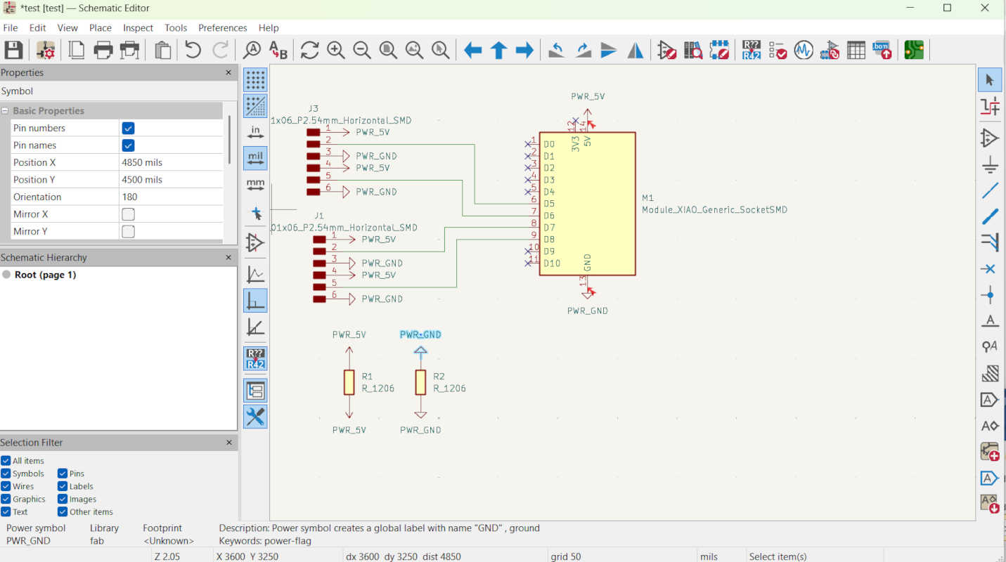
- KiCad is really good about highlighting and showing you connections. When you click on a pin, power, or ground, the program highlights what others it needs to be connected to. Also when creating your paths, if you try to overlap a path, it will not allow you to do so, letting you know you need to redesign your path or connections.
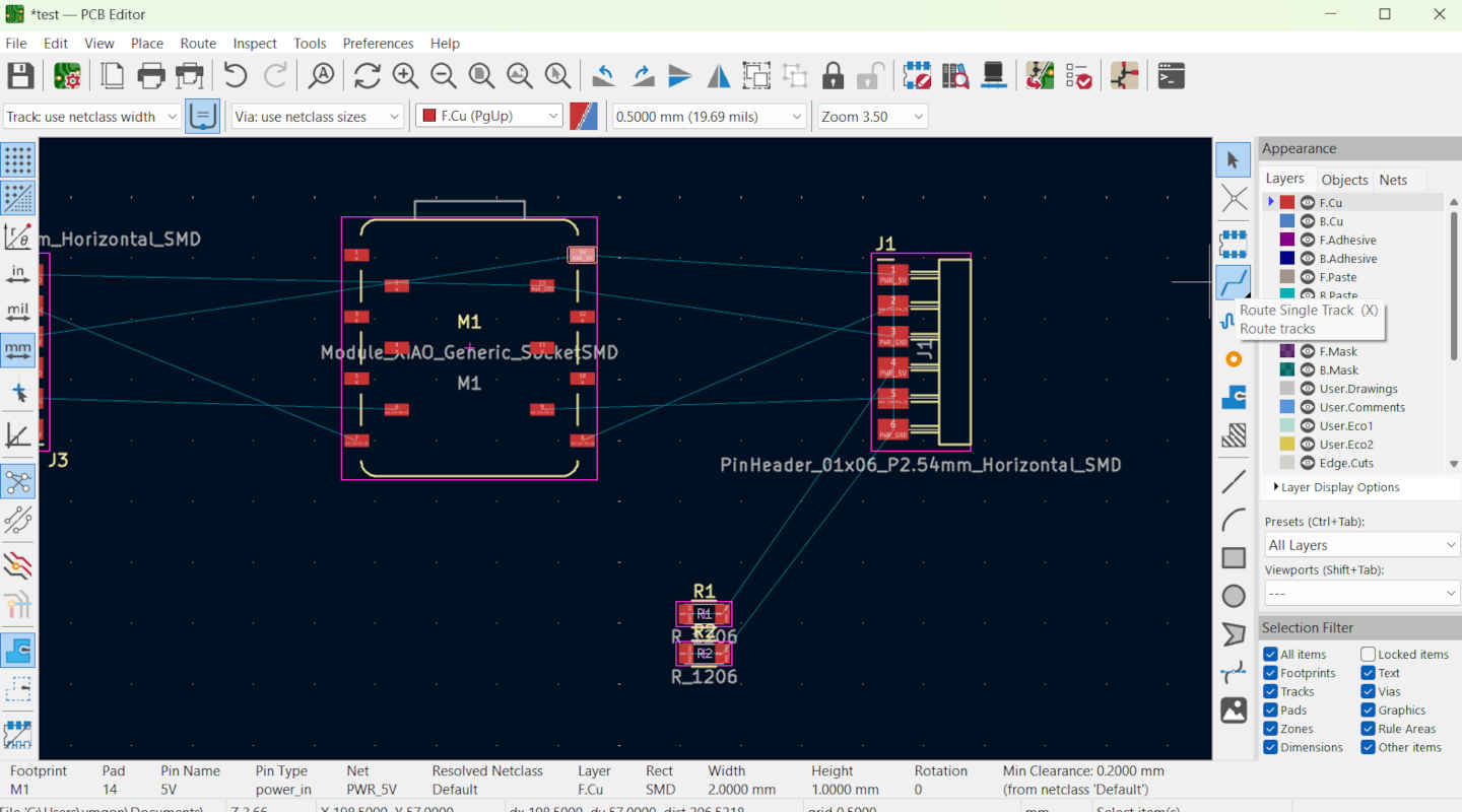
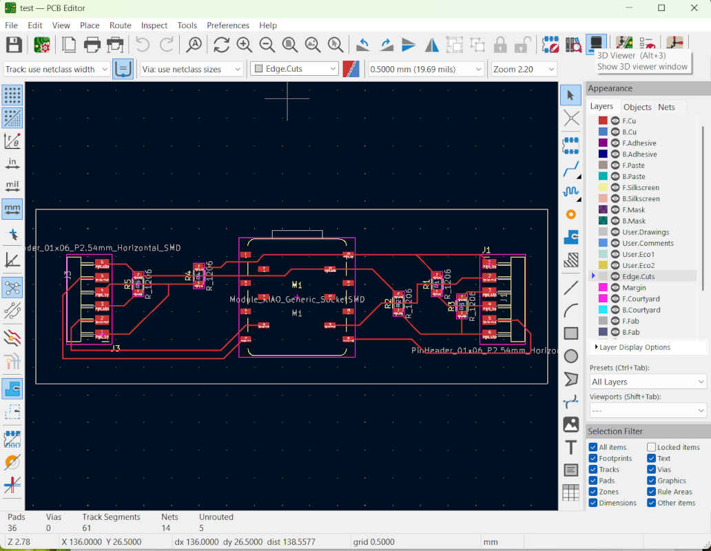
- Designing the paths and figuring out all the different possibilities is tedious yet pretty exciting. Its designing your own puzzle that can be executing in so many different ways. I’ve slowly started exploring different paths and aesthetics, but really plan on playing with it much more and possibly giving it a go by free handing. But that will be later on for future Vicky. For know I just wanted to get a design together that works.
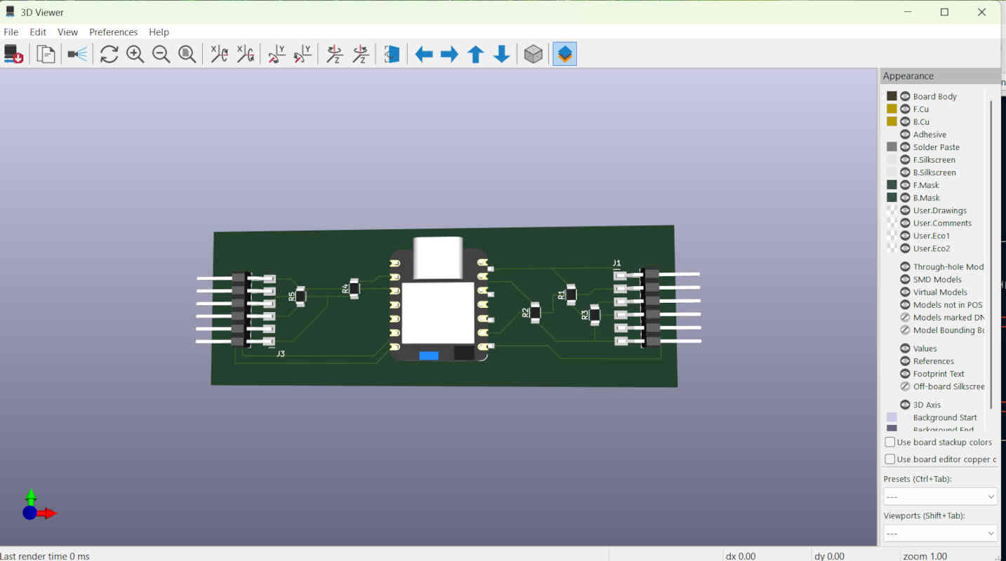
- Once you layout all your connecting paths, you can view your design as a 3D rendering with the 3D viewer button. This gives you a pretty realist idea of how your architecture will physically look.
Group Assignment
To start off with the group assignment we decided to stick with the Quentorres board we had used during Week 4 for Embedded Programming. We retained the hello.button-blink code provided to us by FabAcademy in the microcontroller and used its code as a part of our tests.
- We began by using the multimeter. Incidentally, we discovered that we could short-circuit our board by inadvertently connecting two points or two pins in this case that should not be connected. In short-circuiting the board we caused the board to shut down. Breaking this temporary connection causes the board to turn on again.- Moving forward with the multimeter, we found out that we get two voltage readings. One for when the circuit board has the LED on with a reading of 4.5, and when the button is pressed, which shuts off the LED, the voltage goes down to 1.729 indicating less power usage.
- The oscilloscope was used in the second test. The two green arrows on the screen indicate its base level, the line is at the same level. When the oscilloscope is used to make contact with a part of the board, you can see the line sink downwards. This is representive of the voltage being used to in the board. The LED in the board is always powered on unless you press down on the button. When the button is pressed it shuts off the LED, less voltage is being used and this is seen in the video when the line slightly moves upwards. Ending contact springs the line back up to its original position. These results mirror the test with the multimeter.