


Individual Assignment:
- Make and test a microcontroller development board that you designed.
- Extra credit: Make it with another process
Group Assignment:
- Characterize the design rules for your in-house PCB production process.
- Submit a PCB design to a board house.
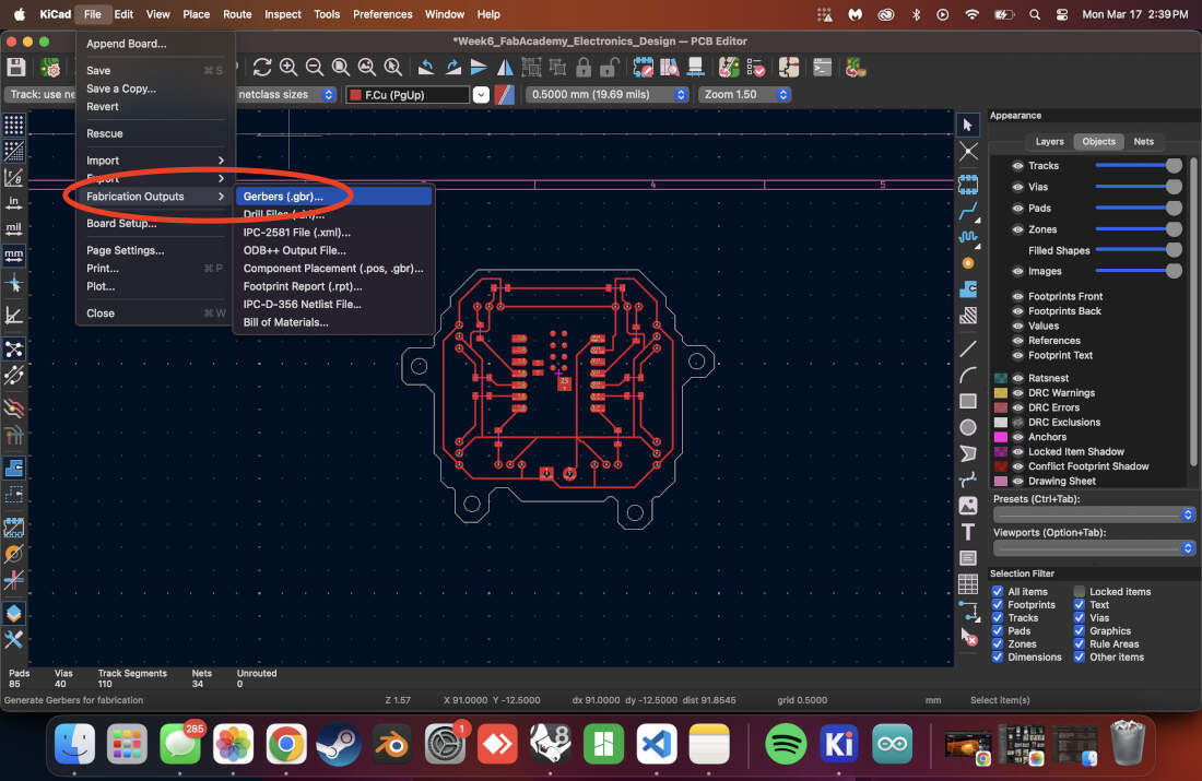
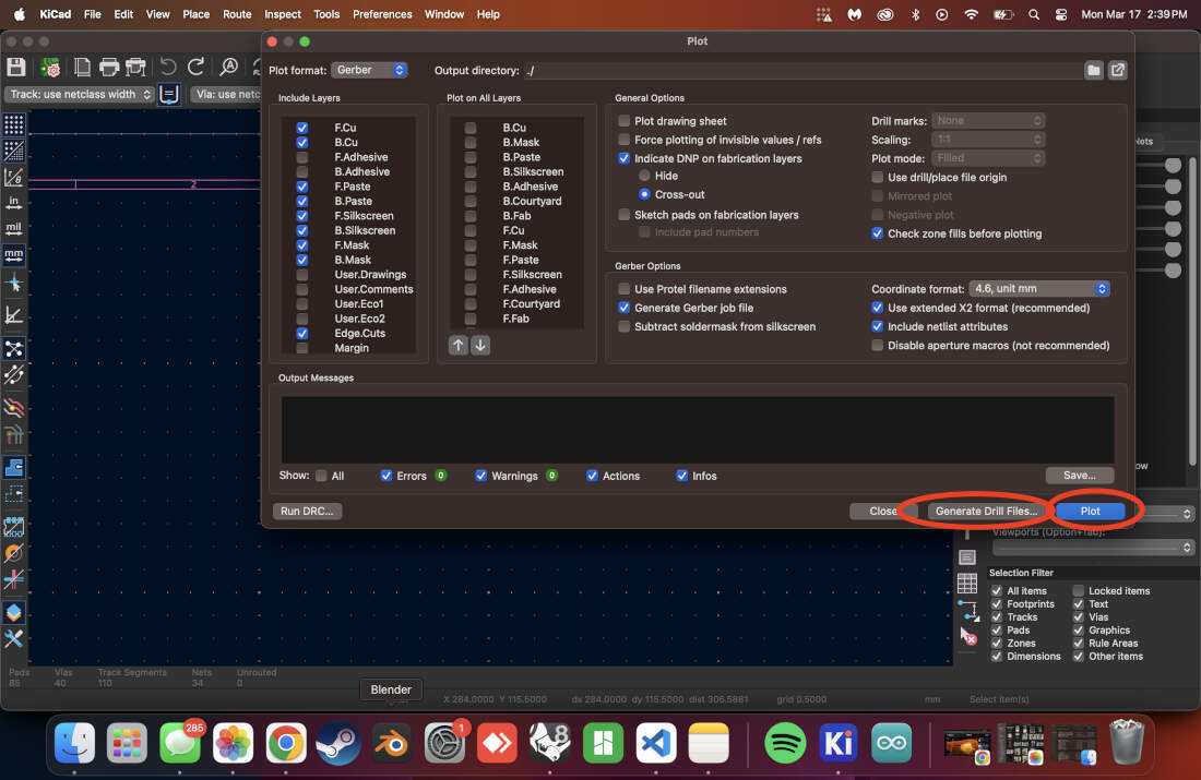
To begin producing my own PCB board I have to begin by exporting my Gerber and Drill files from KiCAD. To do so I have to go into KiCAD's fabrication outputs under the File tab, select the appropriate output directory for the gerber files, doing the same for the drill files and generating them, and then plotting the gerber files to complete the exports.
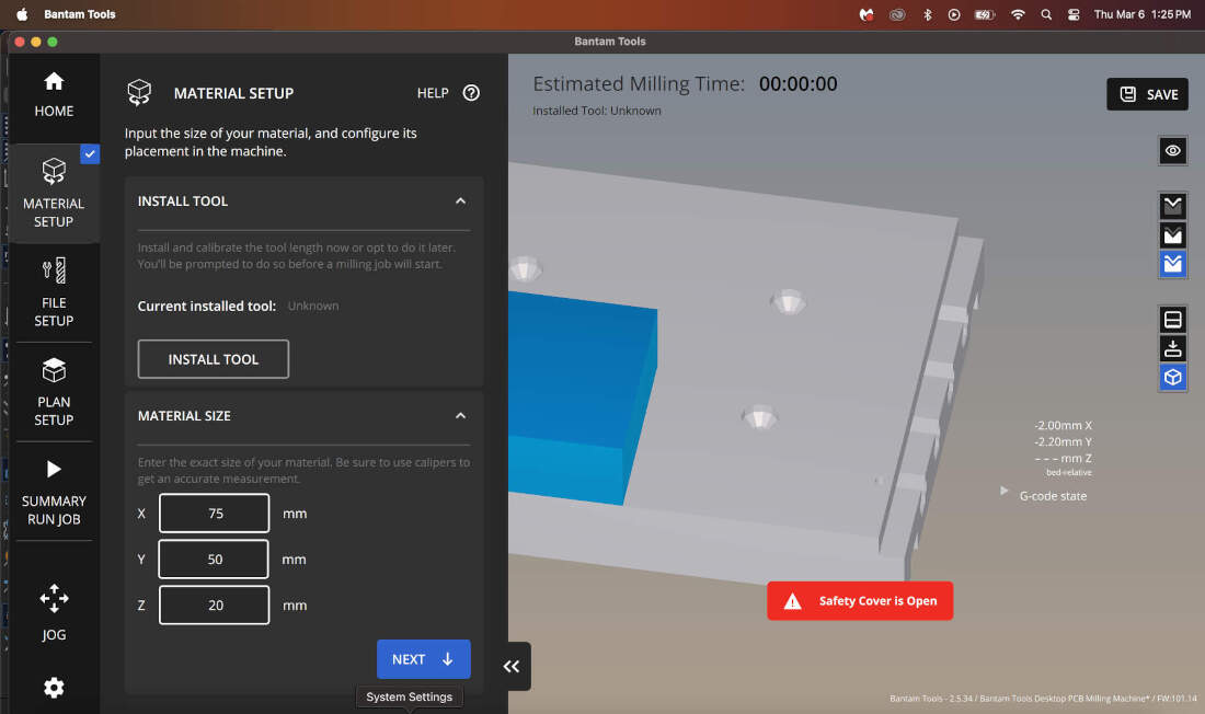
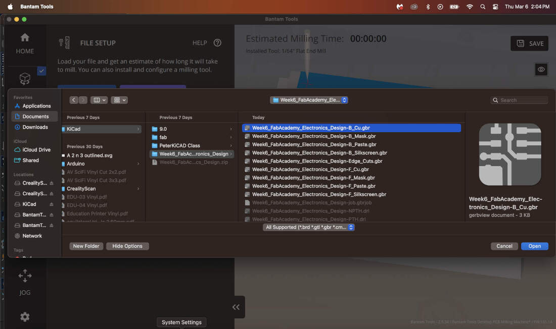
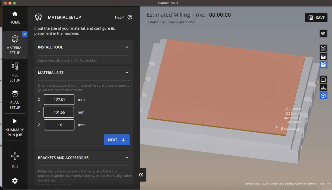
To mill my board, I downloaded the Bantam Tools Milling Machine Software because we have a discountinued version of the Bantam Tools PCB Milling Machine. In the software, we are prompted to install the tool of our choice. In my case I chose a 1/64 flat end mill. Additionally I measured the FR-1 copper clad boards with a caliper. I inputted the measurements into the program so that the materials dimensions would be simulated.
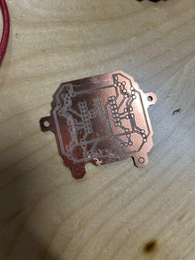
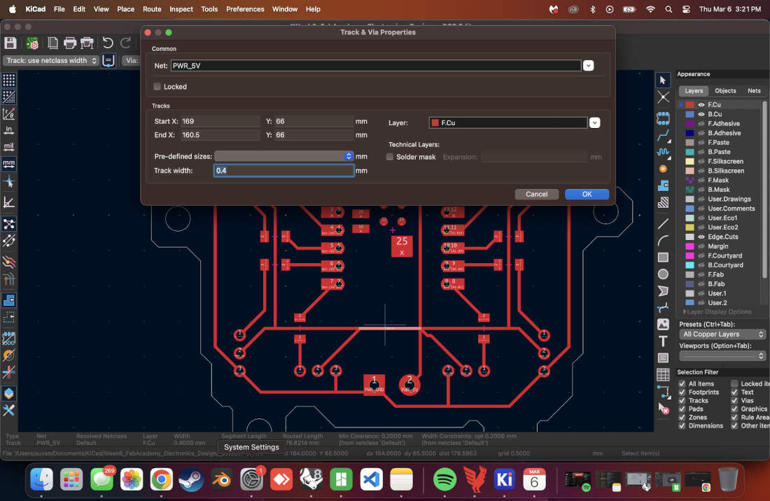
The following step is the file setup. This is one of the many mistakes I made this week. Normally the first file one would have to upload in this section is the "-F-Cu.gbr" file. Instead I upoaded the "-B-Cu.gbr" file. The "f" is the front or the top of the board and the "b" is the back or bottom of the board. I did not know this. I also did not know the difference between NPTH and PTH drill files, so the NPTH file remained where it was. I proceeded with this file setup and used double-sided tape to adhere my board onto the metal plate in the mill. After installing it inside the mill, I ran the file and the last slide shows my mistake. In trying to fix the error I had made by uploading/milling the "-b-Cu.gbr" file, I also milled the "-f-Cu.gbr" thinking that the board would be fine once it had all its paths made. I was wrong because the first file cuts off all connections in the first place as seen with the last image. The paths I had milled were also too thin, so I went back into KiCAD and doubled the thickness of these paths. I also forgot about placing vias in my first KiCAD design, so I did not get any vias in the physical board which led to me discovering that I had to place vias in the file in the first place.
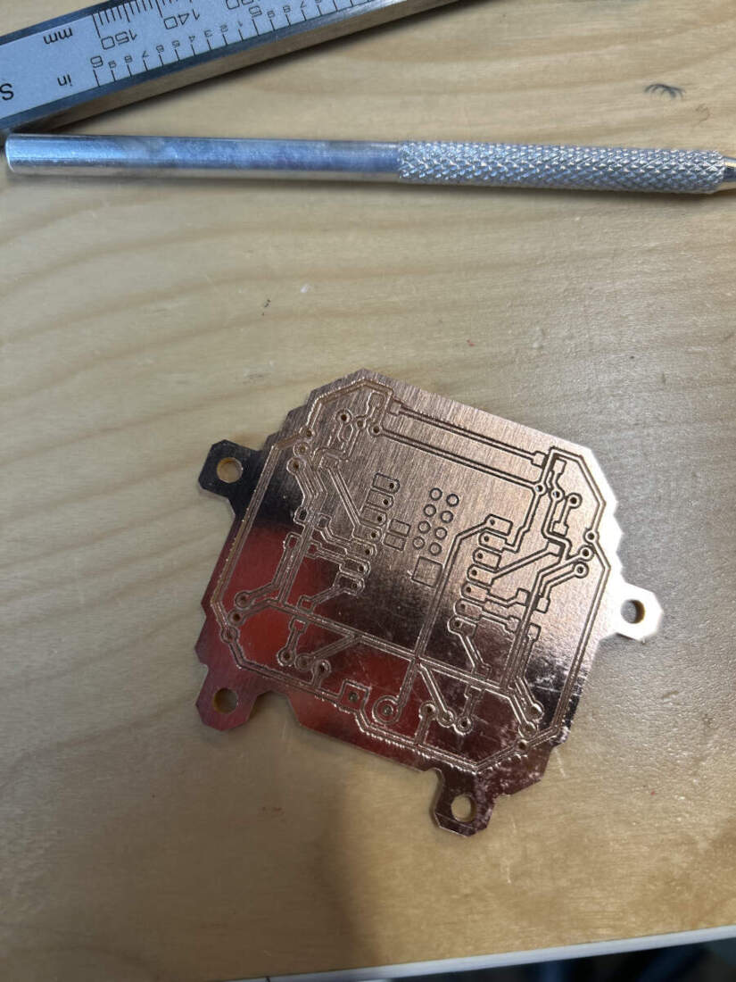
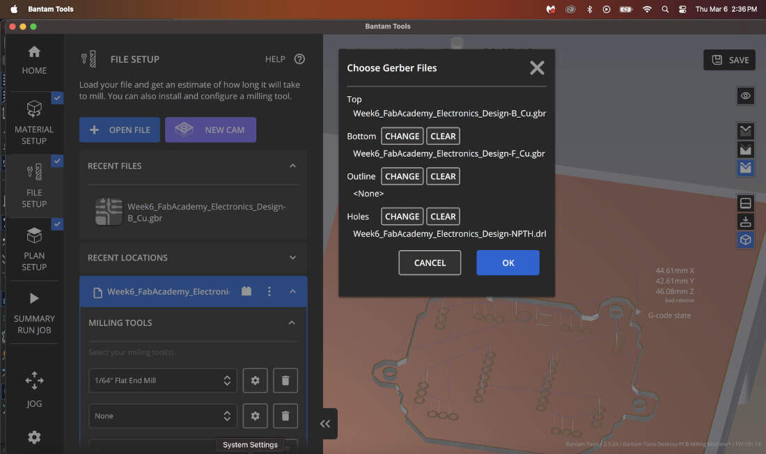
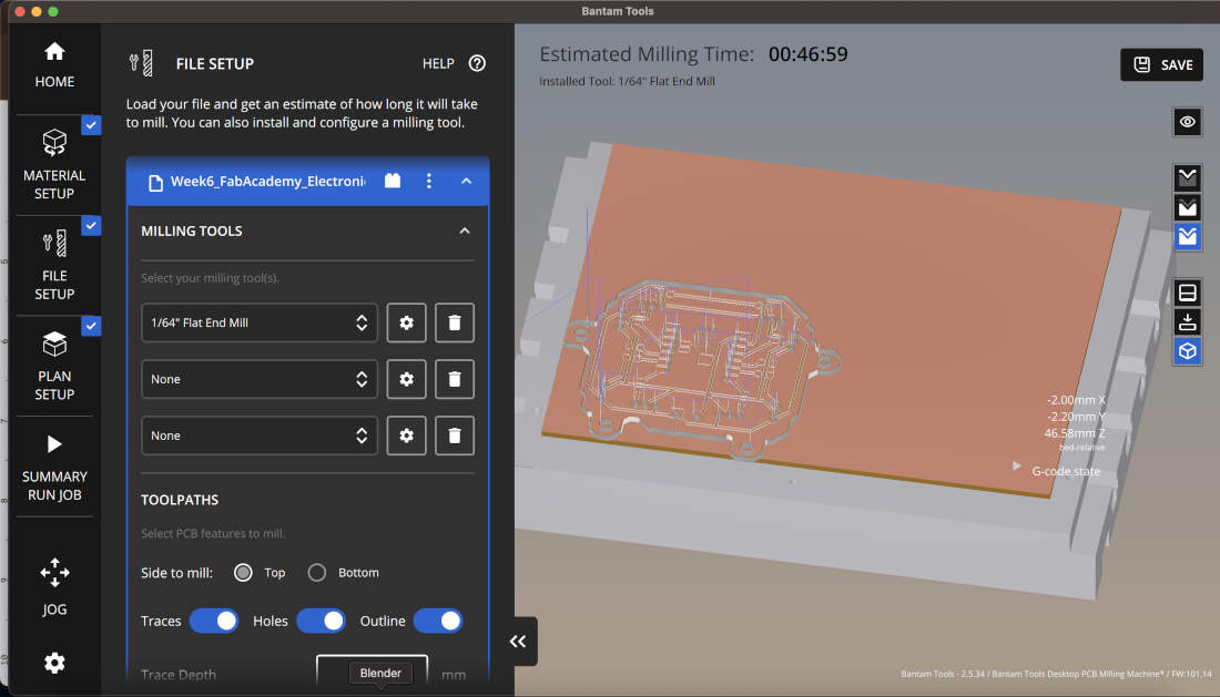
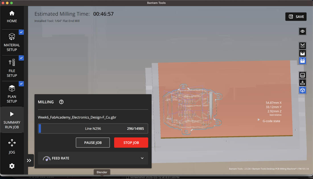
As mentioned previously the track width was doubled in KiCAD. To ensure I did not repeat the same mistakes I made sure to start by uploading the "-F_Cu.gbr" file first, ignoring the "-B_Cu.gbr" because I did not have one. I uploaded my edge cuts or outline cuts and then I uploaded the correct drill file. While in the software I also get warned about possibly needing a smaller tool for some of my cuts. This can be ignored though since this warning pops up because angles cannot fully be formed with straight lines in some instances. I ran the file and you can see the final result in the last slide. The paths and connections are solid. The vias are present. Overall a pretty good board to proceed with.
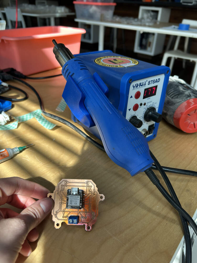
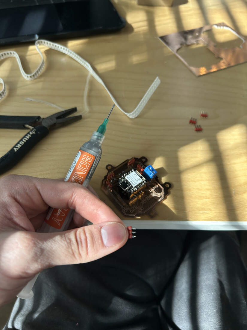
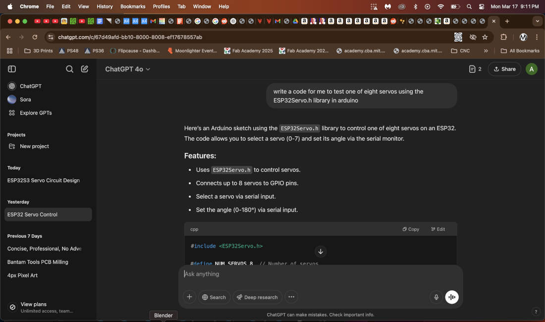
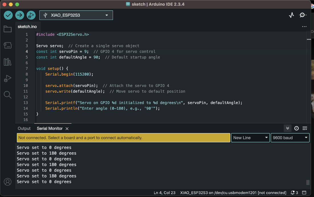
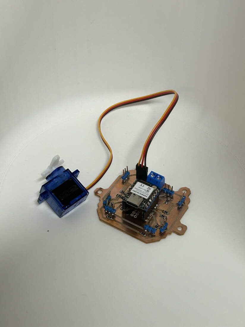
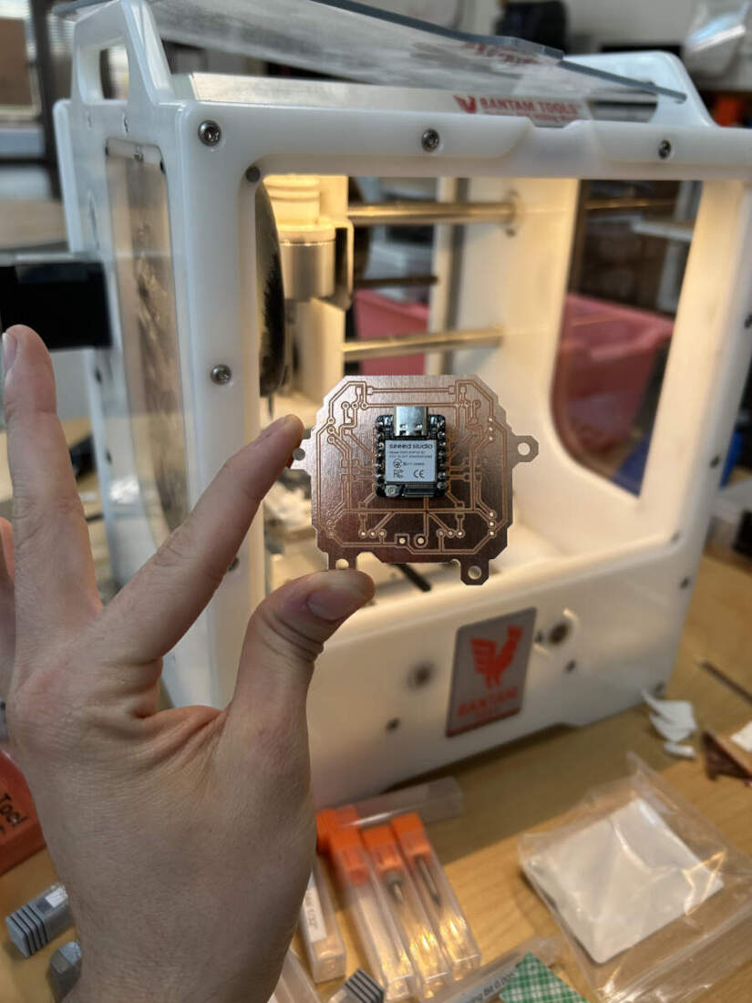
I started soldering my components onto the board by using a hot air gun and soldering paste. I would lay the paste either into the board or onto the pins on the components and then I would blast the soldering paste with 450 degrees of hot air. I was able to complete my first board this way. I inevitably fried the ESP32S3 on this board though. I think I crossed the multimeter rods I was using some wrong way and my board ended flashing red all the time. I went with my weird hunch and decided to proceed with milling and soldering another board and ESP32S3. This one worked perfectly. I asked ChatGPT to create some basic servo testing code for me and I pasted it into the Arduino IDE. This code served its purpose as it allowed me to test every single one of the relevant GPIO's attached to a servo by using the router terminal in the IDE to command the servos to change their angle. Eight of eight servos worked perfectly which made me really happy as this was my first time every making a functional PCB. All I had to do was change the GPIO pin I was interacting with to test each slot. Source code attached below.
    #include <ESP32Servo.h>

    // Create a single servo object
    Servo servo;

    // GPIO 9 for servo control
    const int servoPin = 9;

    // Default startup angle
    const int defaultAngle = 90;

    void setup() {
        Serial.begin(115200);

        // Attach the servo to GPIO 9
        servo.attach(servoPin);
        servo.write(defaultAngle);

        Serial.printf("Servo on GPIO %d initialized to %d degrees\n", servoPin, defaultAngle);
        Serial.println("Enter angle (0-180), e.g., '90'");
    }

    void loop() {
        if (Serial.available()) {
            String input = Serial.readStringUntil('\n');
            input.trim();

            int angle;
            if (sscanf(input.c_str(), "%d", &angle) == 1) {
                if (angle >= 0 && angle <= 180) {
                    servo.write(angle);
                    Serial.printf("Servo set to %d degrees\n", angle);
                } else {
                    Serial.println("Invalid input. Enter a value between 0 and 180.");
                }
            } else {
                Serial.println("Invalid format. Example: '90' to set the servo to 90°.");
            }
        }
    }
For both the individual and group assignments this week we are using the Bantam Tools Desktop PCB Milling Machine to mill PCBs from copper sheets using a 1/64" flat end mill.
Starting off, we made use of the following tools, materials, and software for this process -
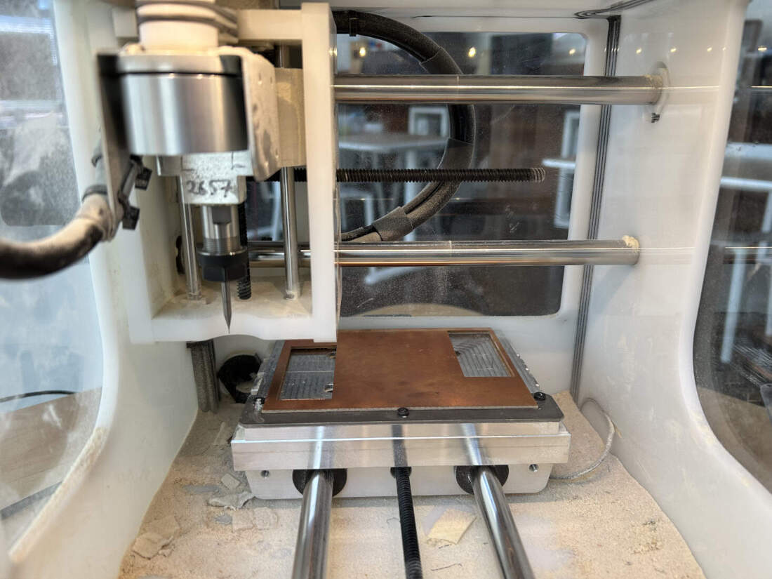
We turned on our PCB mill and opened up the software. We loosened the collet and then installed and tightened the 1/64” Flat End Mill we wished to use and we made sure to use double-sided tape to adhere the copperboard, the material of the circuit board, onto the CNC plate.
Using Calipers we measured the board’s length, width, and thickness and inputted the info into the software. Additionally we also measured the thickness of the tape and programmed an additional Z-offset due to the height of the tape.
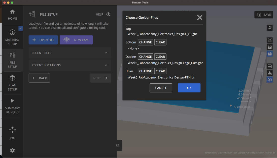
The next step in the process is importing your PCB Gerber files (.gbr) into the Bantam Tools software. When doing so you have to make sure to start off with selecting your file ending in “-F_Cu.gbr” first as the “F” means front and in the software translates into the Top of the PCB. If you had a back to your PCB, you would flip it over and make sure that you upload your “-B_Cu.gbr” file into the Bottom slot, but we do not have to worry about that here. Uploading the “-F_Cu.gbr” is only the start, to upload the outline, the perimeter of your PCB that is to be cut, you have to upload the “-Edge_Cuts.gbr” file. If your PCB has holes then upload the “-PTH.drl” file to cut out your PCB’s vias or drill holes.

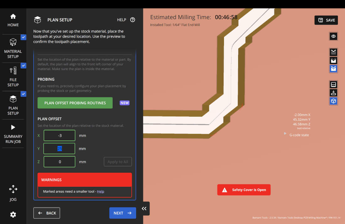
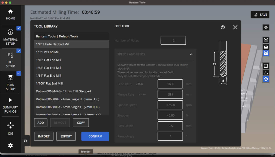
Once the files are uploaded you can assign the 1/64” end mill for the traces, pads, vias, and outline. You also have the option of involving other end mills in the process if you so choose. You can also edit the Toolpaths by altering which side you are milling, trace depths and clearances, or the rotation of the board itself. Depending on the end mill you choose, you can also further edit feed rate, plunge rate, spindle speed, stepover, pass depth, and ramp angle.
When the G-code is generated, the software simulates your design and warns you if traces are too close together to prevent shorts or if there are other errors in your design.
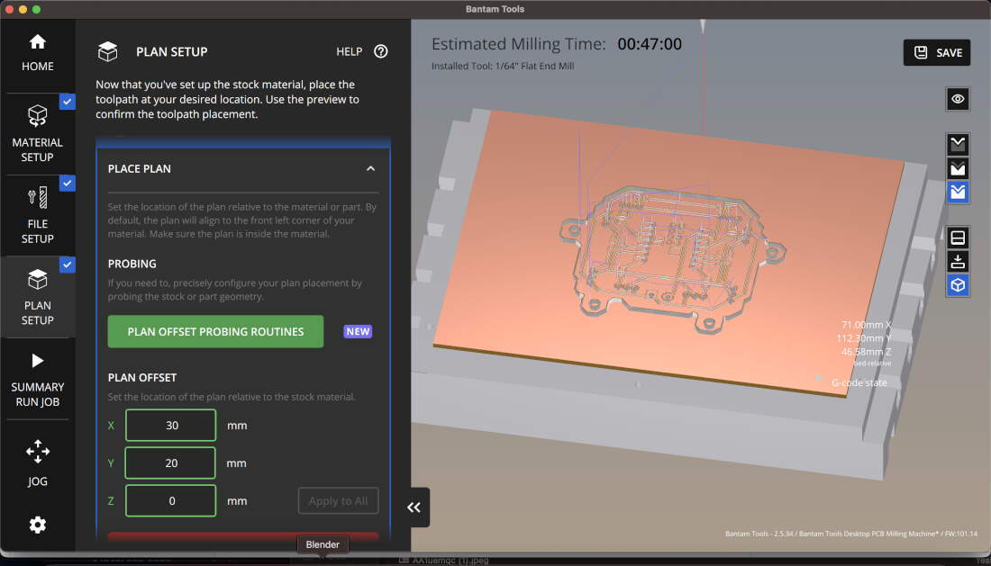
After the file set-up you only need to offset your design so you can mill it where you choose to. Don’t inefficiently mill it out in the middle of the board like in the visual. That is just for show but if milled out there it would be a waste of material.
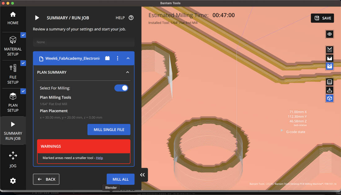
Once you're satisfied with the settings, you can send the board to the mill. If you receive warnings like those shown above, they may indicate legitimate design flaws that need correction. However, in some cases, they are superficial, occurring because the CNC cannot create sharp angles and instead fillets them.
Monitor the board, ensure there is a proper cut depth, pause to adjust if necessary, and when done, inspect the traces to ensure they are fully and properly cut with shard edges. If needed, and if the board has remained in the same position as before, you can do a second pass at deeper settings.
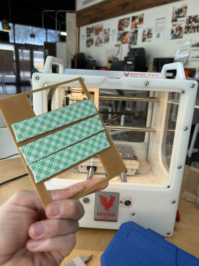
Remove the PCB from the mill plate upon job completion. Pry it upwards with a flat tool and avoid bending or cracking the board, it is very delicate. Wipe the PCB with isopropyl alcohol to remove debris, and a fine bristle brush also helps.
Using a multimeter to check that traces are correctly isolated is a good move. Shorts, if any are present, can be fixed with a knife or fine sandpaper.
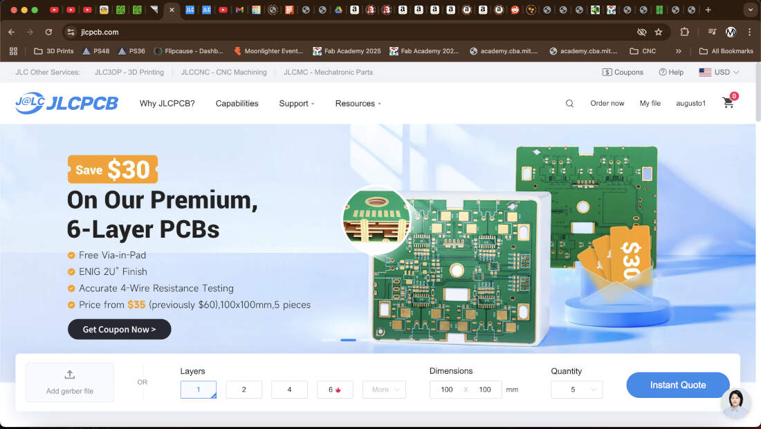
The board house we chose was JLCPCB. Based on some reviews we’ve read it seems like a rather reputable website with a user friendly interface. It was really simple right off the bat. We chose to get started with a quote by uploading a zip folder with our gerber files and selecting the 1 layer PCB option.
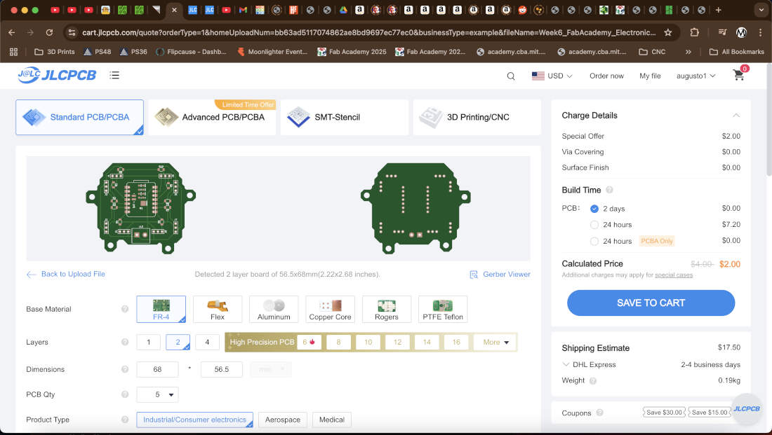
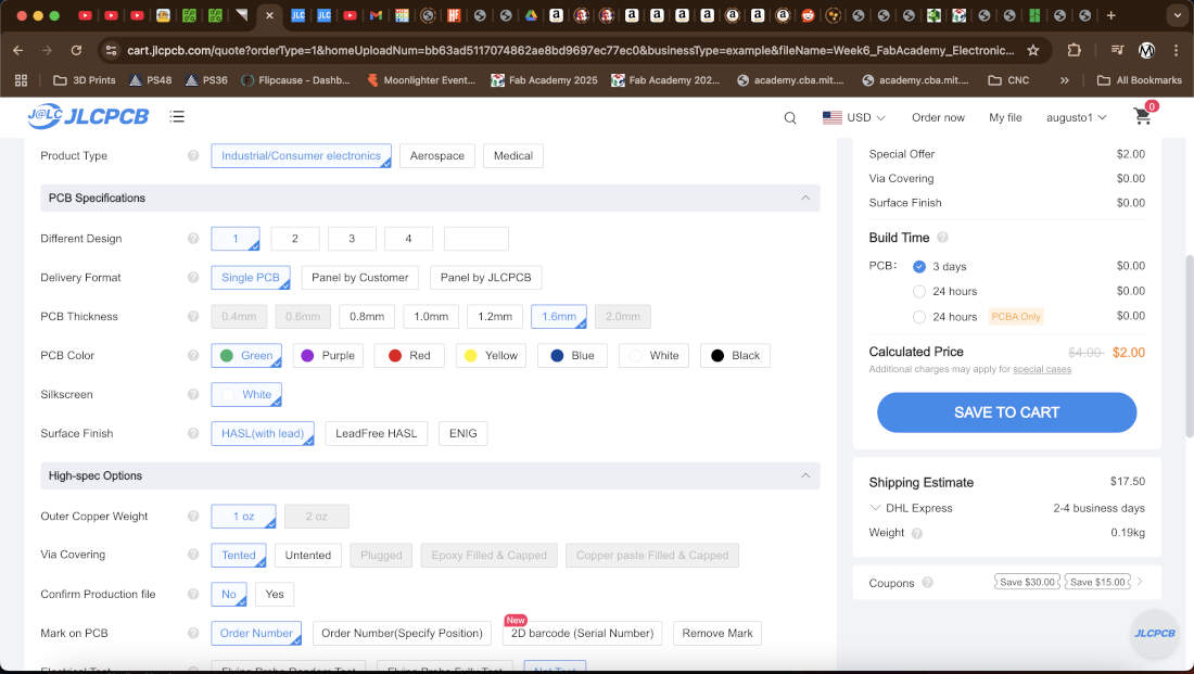
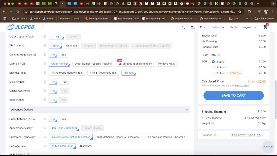
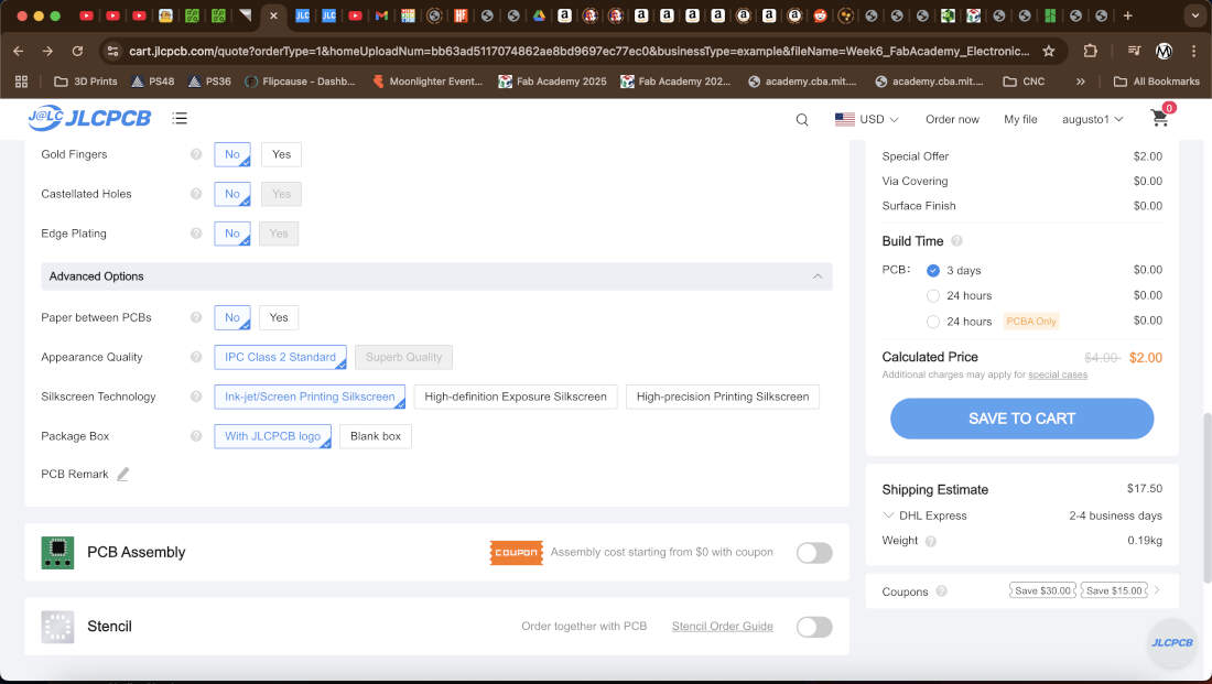
The interface was really easy to navigate and all we had to do was switch over to a 1 layer PCB option again. Everything else was left on the default options. JLCPCB automatically calculates the dimensions of your board based on the files uploaded. I can alter the board thickness if needed and I can change the color of the PCB for an upcharge.
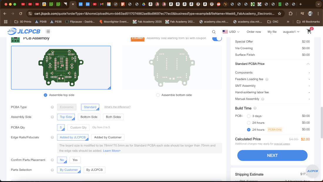
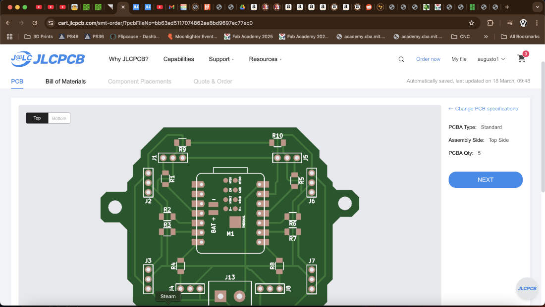
I can also request that my PCB gets assembled based on the components library that JLCPCB may have available at the given moment. Either the top or bottom sides can be assembled with the options chosen. If assembly is chosen, you’d have to secure a Bill of Materials and information regarding the designation and component position so that the manufacturer can properly source your parts and assemble them in the correct locations.
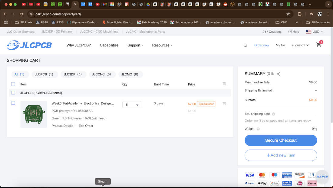
Once you’re satisfied with all the options selected, you can save your order to your cart and then secure your checkout. You’d proceed with inputting all your card and address information and finalize the transaction as you usually do everywhere else.
Copyright 2025 Augusto Vanegas - Creative Commons Attribution Non Commercial Source code hosted at gitlab.fabcloud.org