Electronics Production
Back to HomeGoals
group assignment
- characterize the design rules for your in-house PCB production process
- submit a PCB design to a board house
Individual Assignment
- make and test a microcontroller development board that you designed
- extra credit: make it with another process
Group Assignment
Design Rules for in-house PCB production process
Machines and Tools
The equipment used in Litchee’s studio for PCB fabrication is the Snapmaker.
Official website: https://www.snapmaker.cn/
Snapmaker is a versatile 3-in-1 desktop manufacturing tool that integrates 3D printing, laser engraving, and CNC carving in one machine. With its sleek design and intuitive operation, it is ideal for makers, designers, educators, and labs. Its innovative modular design allows users to easily switch between different work modules to meet a wide range of creative needs.
Key Features
3D Printing Function:
- Supports FDM (Fused Deposition Modeling) technology, capable of printing with various plastic materials such as PLA, ABS, and TPU.
- High printing precision, suitable for producing small, accurate models, prototypes, and complex designs.
- Equipped with an automatic bed leveling function to ensure accurate prints every time.
Laser Engraving Function:
- Supports high-precision laser engraving on wood, leather, plastic, and other materials.
- Adjustable laser power to accommodate different materials and engraving depths.
- Fine laser control system enables detailed engraving, ideal for artistic work, personalized designs, and creative gifts.
CNC Carving Function:
- Supports computer numerical control (CNC) carving for materials like wood, plastic, and aluminum.
- High-precision cutting capability suitable for delicate craftwork or small-batch production.
- Equipped with a powerful drive system, capable of handling complex engraving tasks.
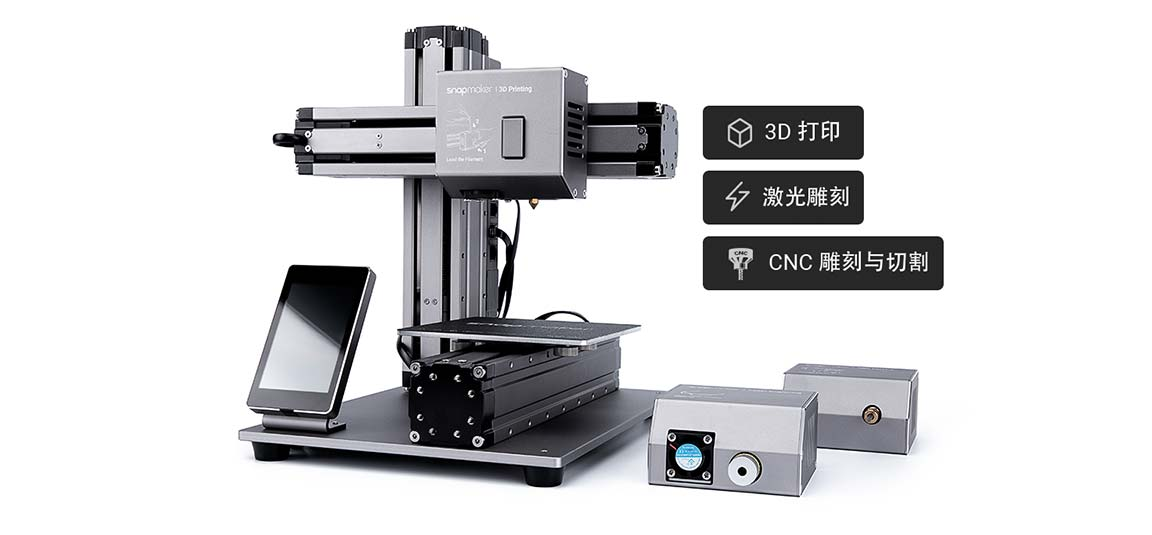
Snapmaker Product Specifications
Basic Parameters
- Machine Size: 335 × 272 × 289 mm
- Net Weight: 5.7 kg
- Body Material: Aluminum Alloy
- File Transfer: USB Drive, USB Cable
- Power Input: 100–240 VAC
- Operating System: macOS, Windows
- Touchscreen: 3.5 inch
3D Printing
- Heated Bed Temperature: Up to 80°C
- Build Volume: 125 × 125 × 125 mm
- Head Movement Speed: Up to 100 mm/s
- Nozzle Diameter: 0.4 mm
- Nozzle Temperature: Up to 250°C
- Layer Thickness: 0.05 – 0.3 mm
- Supported Materials: 1.75 mm PLA, ABS, etc.
- Unsupported Materials: Nylon with aluminum powder, graphite, etc.
- Supported File Types: STL, OBJ
- Software: Snapmakerjs, Cura, Simplify 3D, Slic3r, etc.
Laser Engraving
- Working Area: 125 × 125 mm
- Laser Power: 200 mW
- Laser Wavelength: 405 nm
- Laser Safety Class: Class 3B
- Supported File Types: SVG, JPEG, PNG, etc.
- Supported Materials: Wood, bamboo, leather, plastic, paper, fabric, non-transparent acrylic, etc.
- Unsupported Materials: Metal, glass, gemstones, transparent or reflective materials
- Software: Snapmakerjs
CNC Carving / Cutting
- Working Area: 90 × 90 × 50 mm
- Tool Shank Diameter: 3.175 mm
- Supported Materials: Wood, acrylic, PCB, carbon fiber board
- Unsupported Materials: Metal, glass, gemstones, etc.
- Spindle Speed: 19,000 RPM
- Supported File Types: SVG, STEP, IGES, IGS, DWG, DXF
- Software: Snapmakerjs, Autodesk Fusion 360, ArtCAM, etc.
*Note: Users can use third-party software such as Autodesk Fusion 360 to convert supported file formats.
Snapmaker PCB Milling Process
As a 3-in-1 desktop manufacturing tool, Snapmaker integrates 3D printing, laser engraving, and CNC carving. Beyond its standard features, Snapmaker can also be used to mill PCBs (Printed Circuit Boards) using the CNC module. The machine provides high precision for operations such as trace isolation and drilling. Below are the steps and principles for milling PCBs with Snapmaker:
Steps to Mill a PCB with Snapmaker
1. Prepare the PCB Design Files:
- Use PCB design software (such as KiCad or Eagle) to create your circuit and export the Gerber files.
- Make sure the files include traces, component placements, and drill holes.
2. Install the CNC Module:
- Attach the CNC carving module to the Snapmaker machine.
- Use a suitable tool head, such as a fine engraving bit or micro drill.
- Adjust the module height to ensure the bit can precisely contact the PCB surface.
3. Secure the PCB:
- Use Snapmaker’s built-in clamps or custom fixtures to hold the PCB in place.
- Ensure the board is flat and stable to avoid any shift during milling.
4. Choose the Right Bits and Tools:
- Select the appropriate tools based on your Gerber files.
- Use fine bits for trace isolation and drill bits for hole making.
5. Set the Machining Parameters:
- Download and install the control software Snapmaker Luban: Download here
- In the software, set parameters such as feed rate, cutting depth, and tool path.
- Adjust settings according to the PCB material and desired precision.
6. Start CNC Milling:
- Load the Gerber files into Luban and start the job.
- Snapmaker will automatically execute the engraving and drilling tasks according to the design.
- It will accurately remove unwanted copper and leave behind the desired circuit paths.
7. Post-processing and Cleaning:
- Inspect the final PCB for clean traces and accurate drill holes.
- Use a brush to remove any remaining debris from the board.
Producing PCB at PCB-house
In the previous week 6 assignment, I created the schematic in JLCPCB EDA.
Introduction to JLCPCB:
JLCPCB (JLC Electronics) is a company that provides one-stop infrastructure services for the electronics industry, headquartered in Shenzhen. Since its establishment in 2006, JLCPCB has been committed to providing cost-effective PCB prototyping, small batch production, SMT assembly, laser stencil, FA mechanical parts, and other services to electronic engineers, research institutions, and enterprises around the world.
Therefore, I can directly open the already saved PCB files in my account and place an order.
Go to the "Order" menu at the top and select "PCB Order" to proceed.
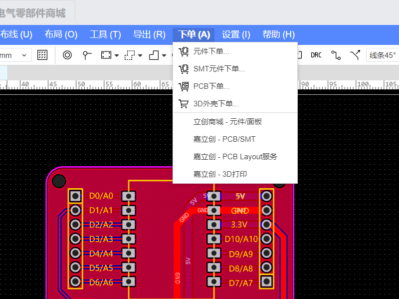
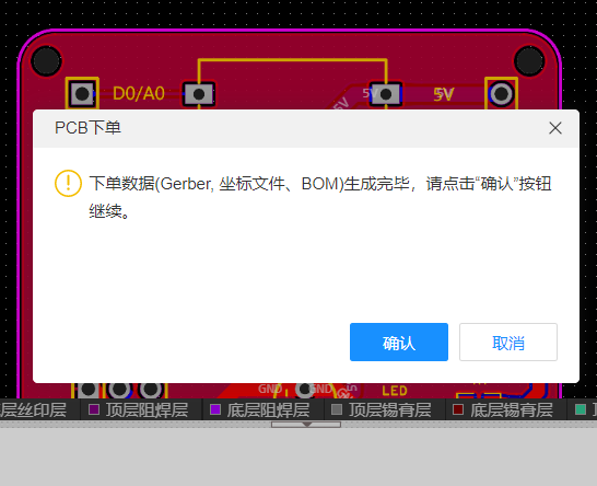
After clicking, the Gerber files, coordinate files, and BOM list will be automatically generated.
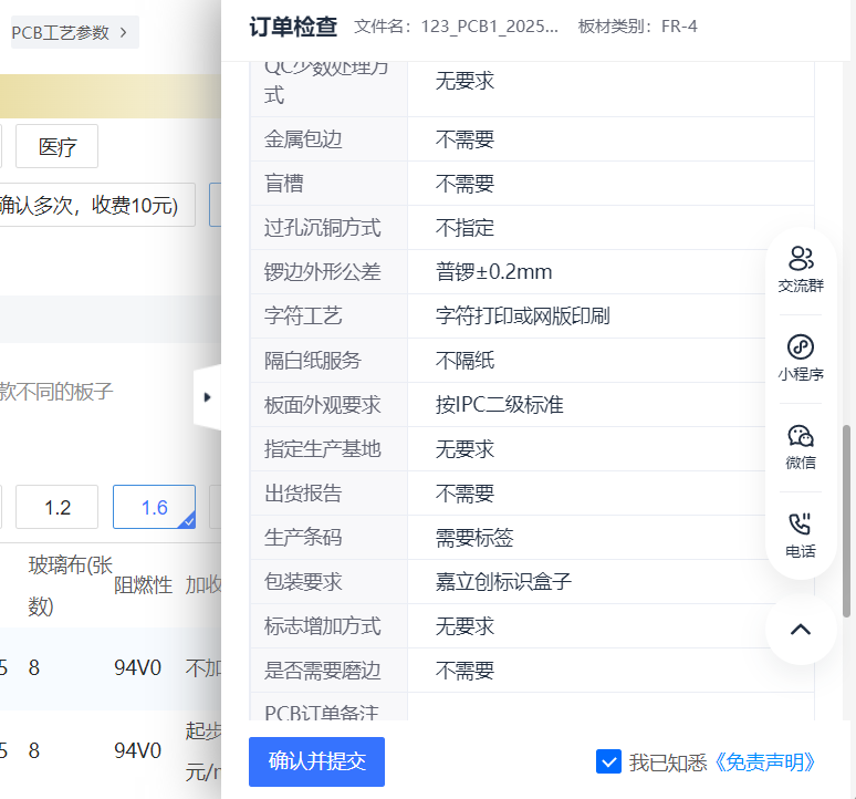
JLCPCB allows online ordering. You only need to confirm the board specifications, which is very convenient.
I chose FR-4 as the board material, and selected the default quantity of 5 pieces, which is free.
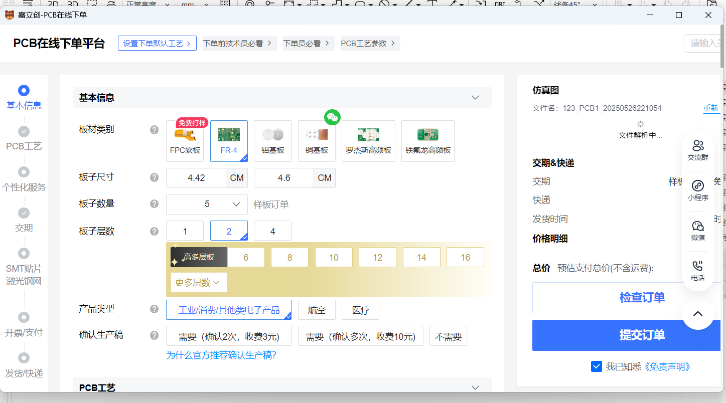
The solder mask layer I designed in week 6 is black, with gold-plated pads.
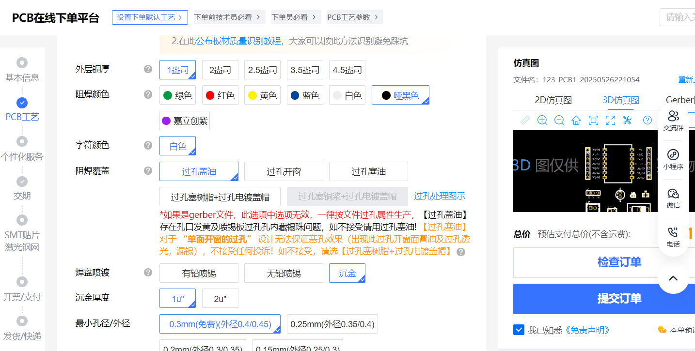
I kept all other settings as default. Finally, I selected the delivery time. Black solder mask takes a little longer, and production can be completed in 3 days.
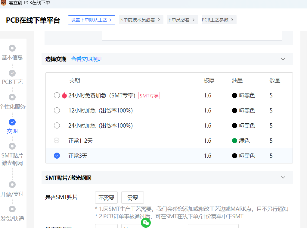
The delivery is also free!!!!
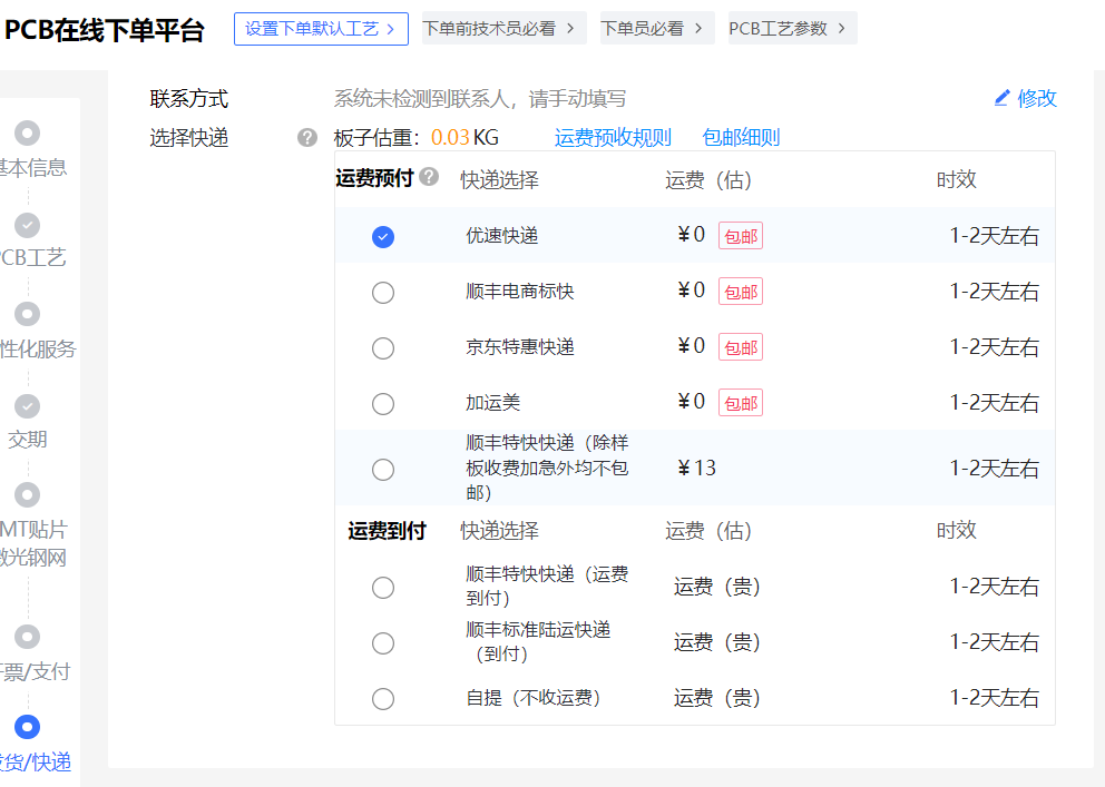
Finally check the order information and it can be submitted.
Individual Assignment
I exported the Gerber file in JLCPCB EDA.
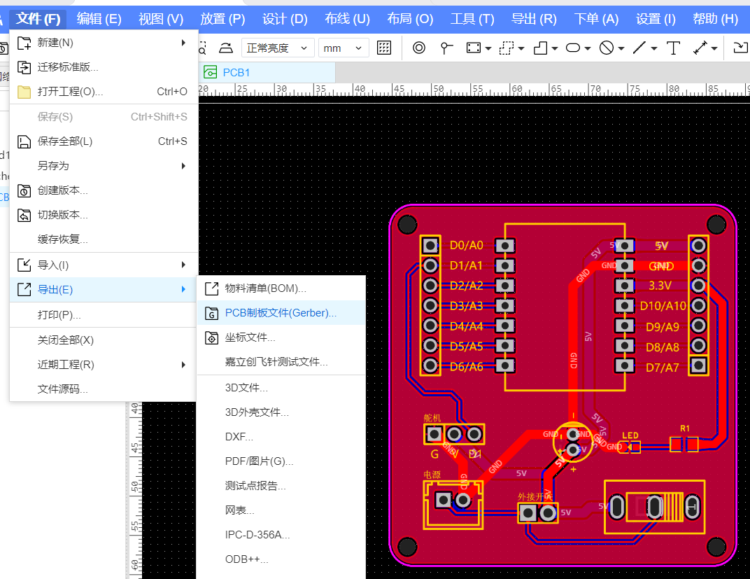
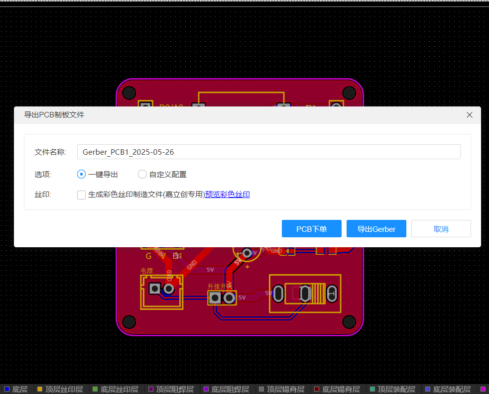
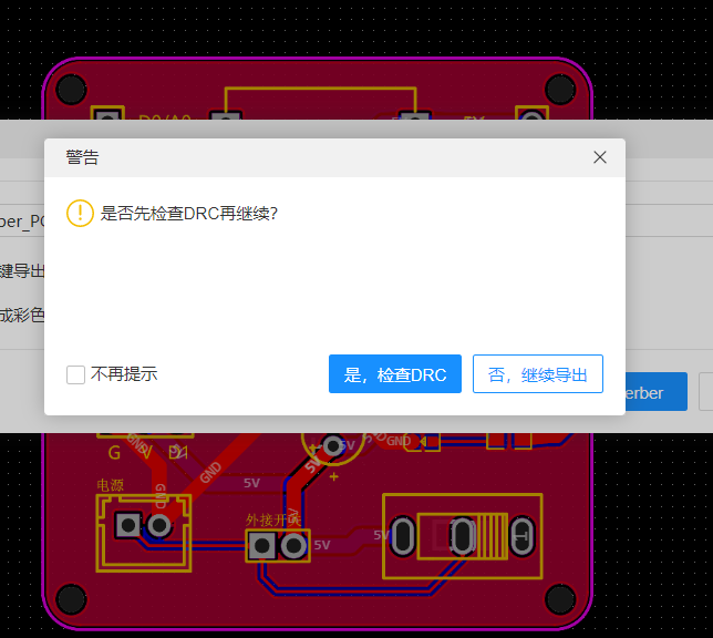
Before exporting, it will prompt to check DRC.
It is exported as a compressed file package.
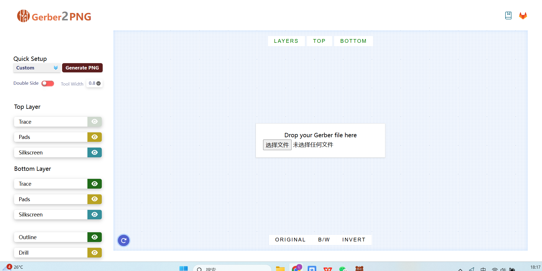
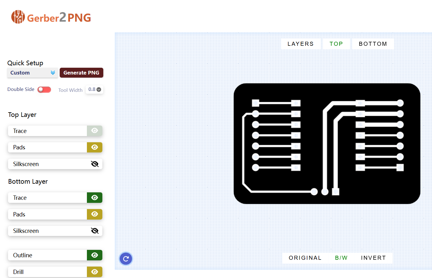
I used Gerber2PNG to generate PNG images from the PCB file.
Website: https://gerber2png.fablabkerala.in/
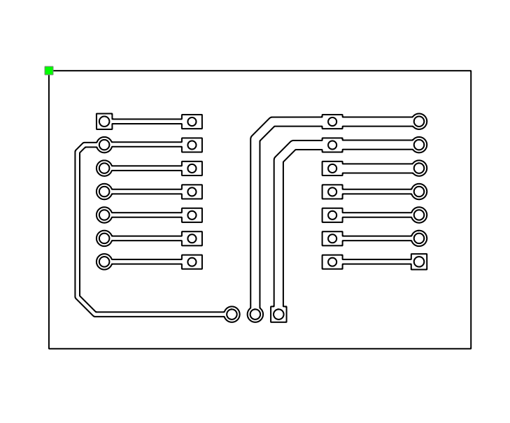
After opening it, I found some problems. The PCB layout I drew in JLCPCB EDA is a two-layer board.
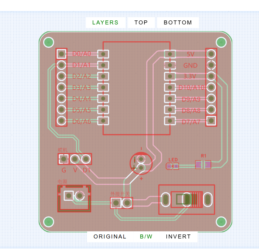
I sent the PCB layout to my friends for review. They pointed out that this part had copper fill, which would require wire-jumping (flywires), and that it needed to be made as a two-layer board. Then, the two layers would need to be combined into one.
Considering that my ability to fabricate a double-layer board is limited and the failure rate would be high, I decided to modify the layout.
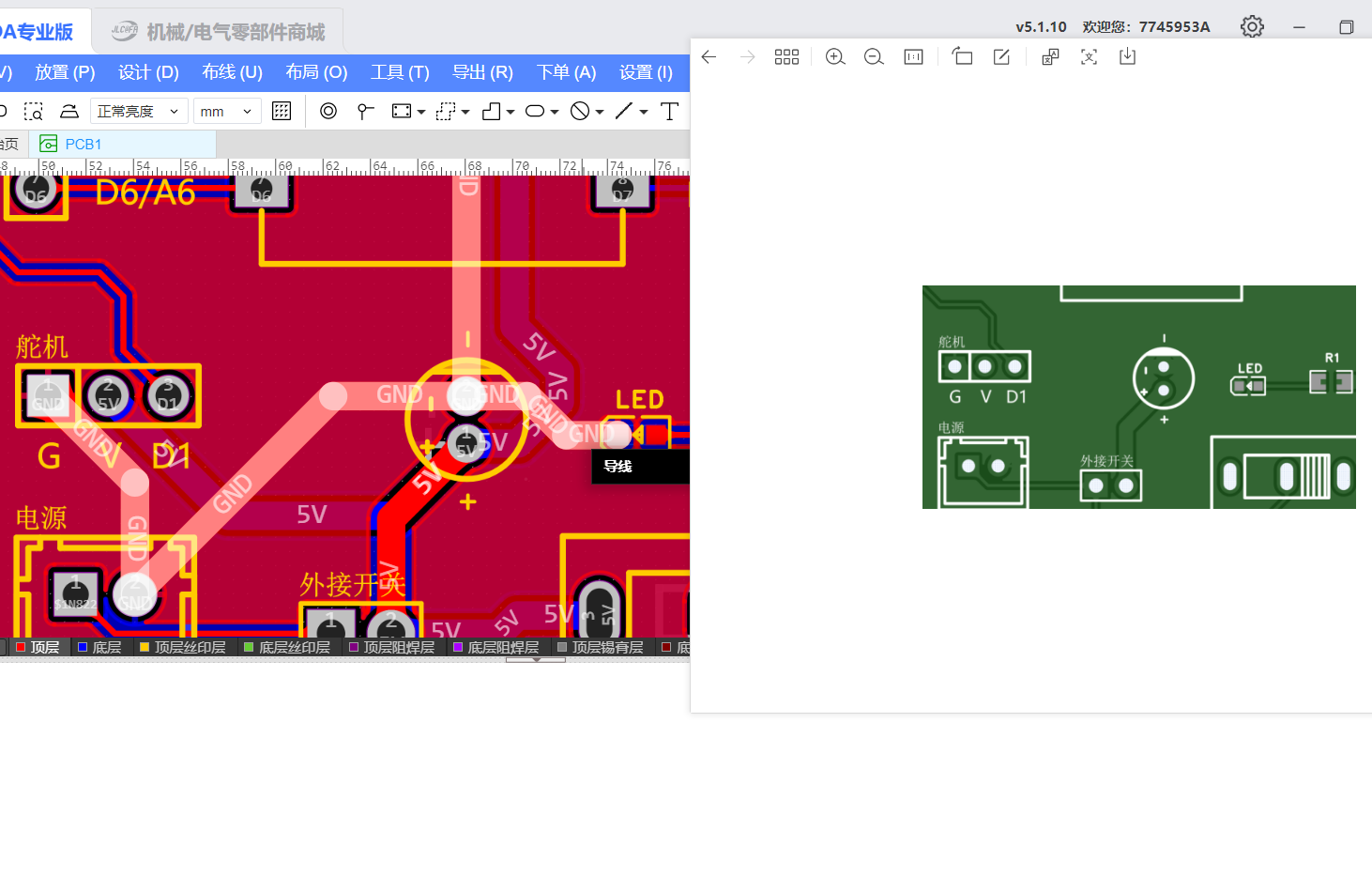
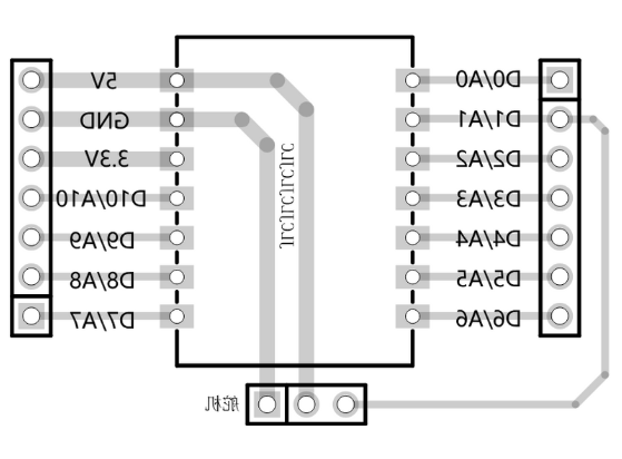
I redrew the layout as a single-layer board and kept only the extended part. Below is the modified schematic:
Schematic file:
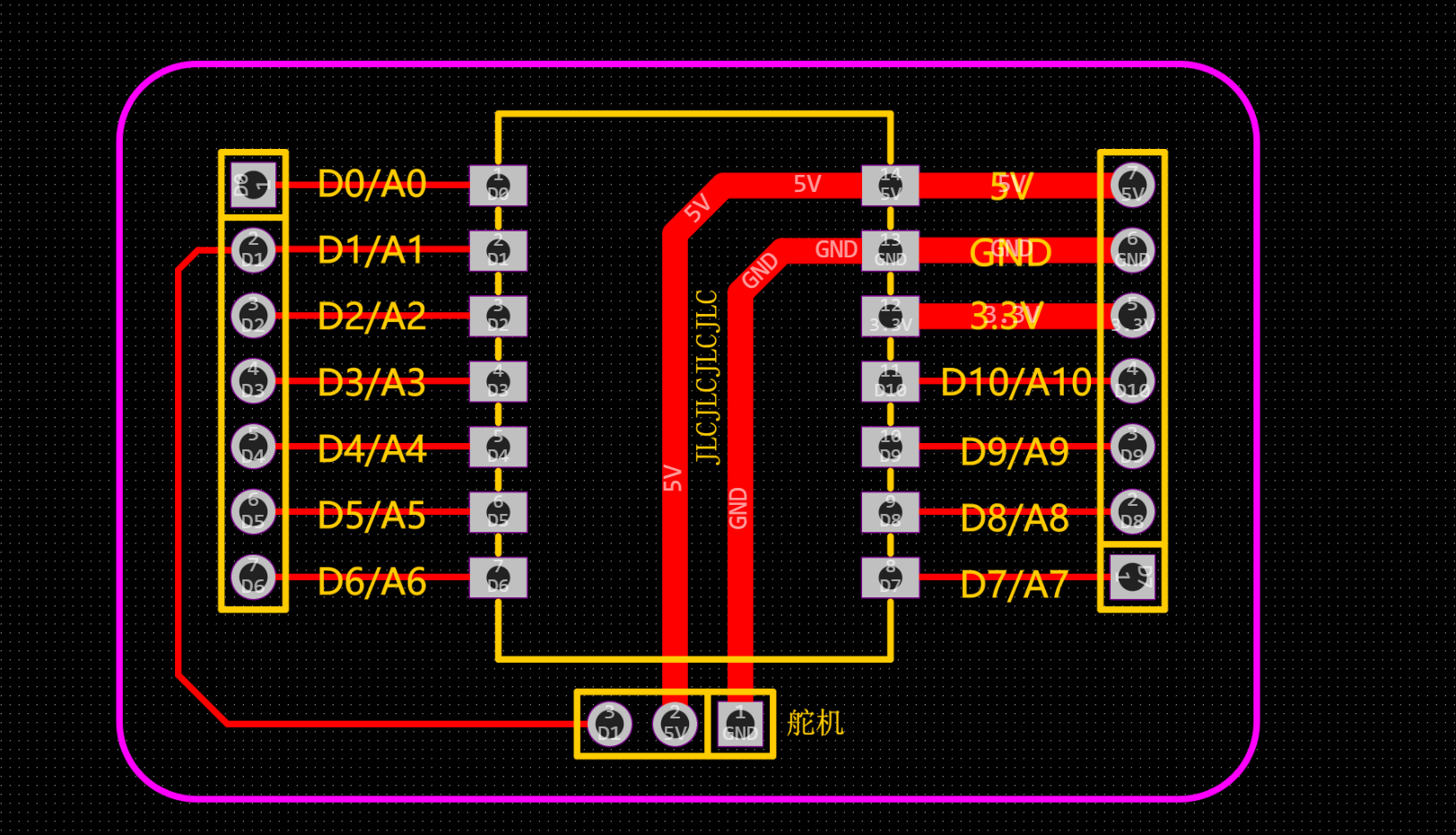
I opened the new design file with Gerber2PNG, and everything looks perfect!
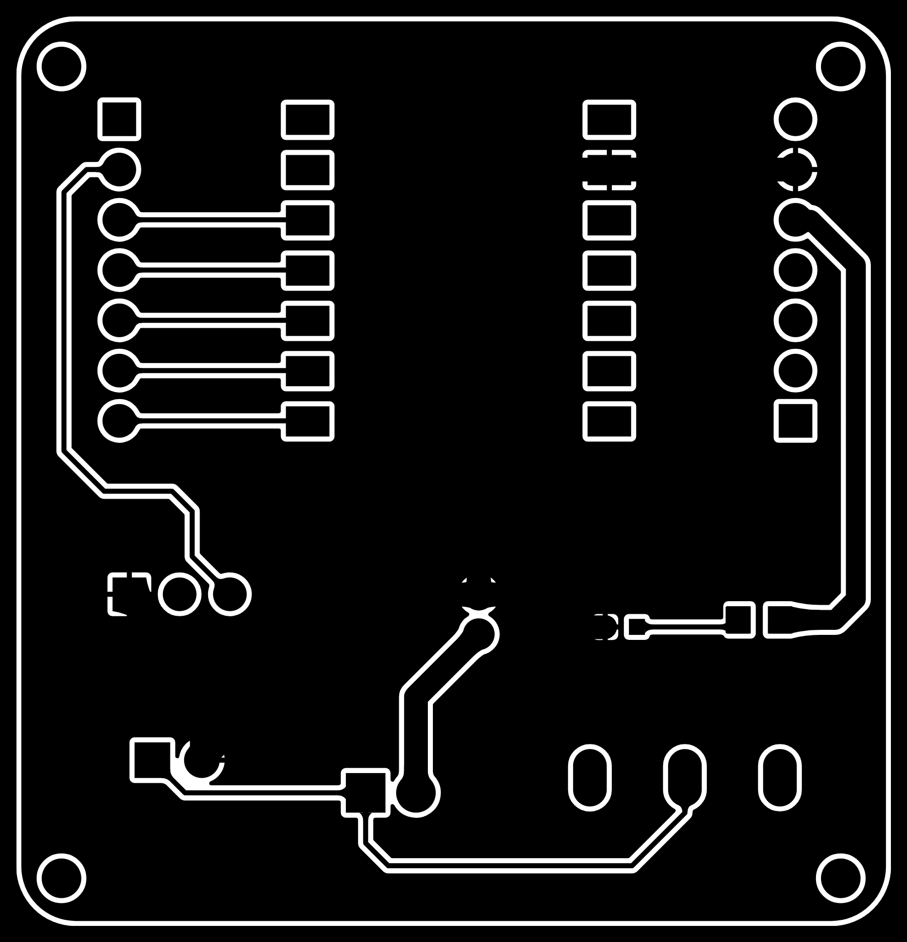
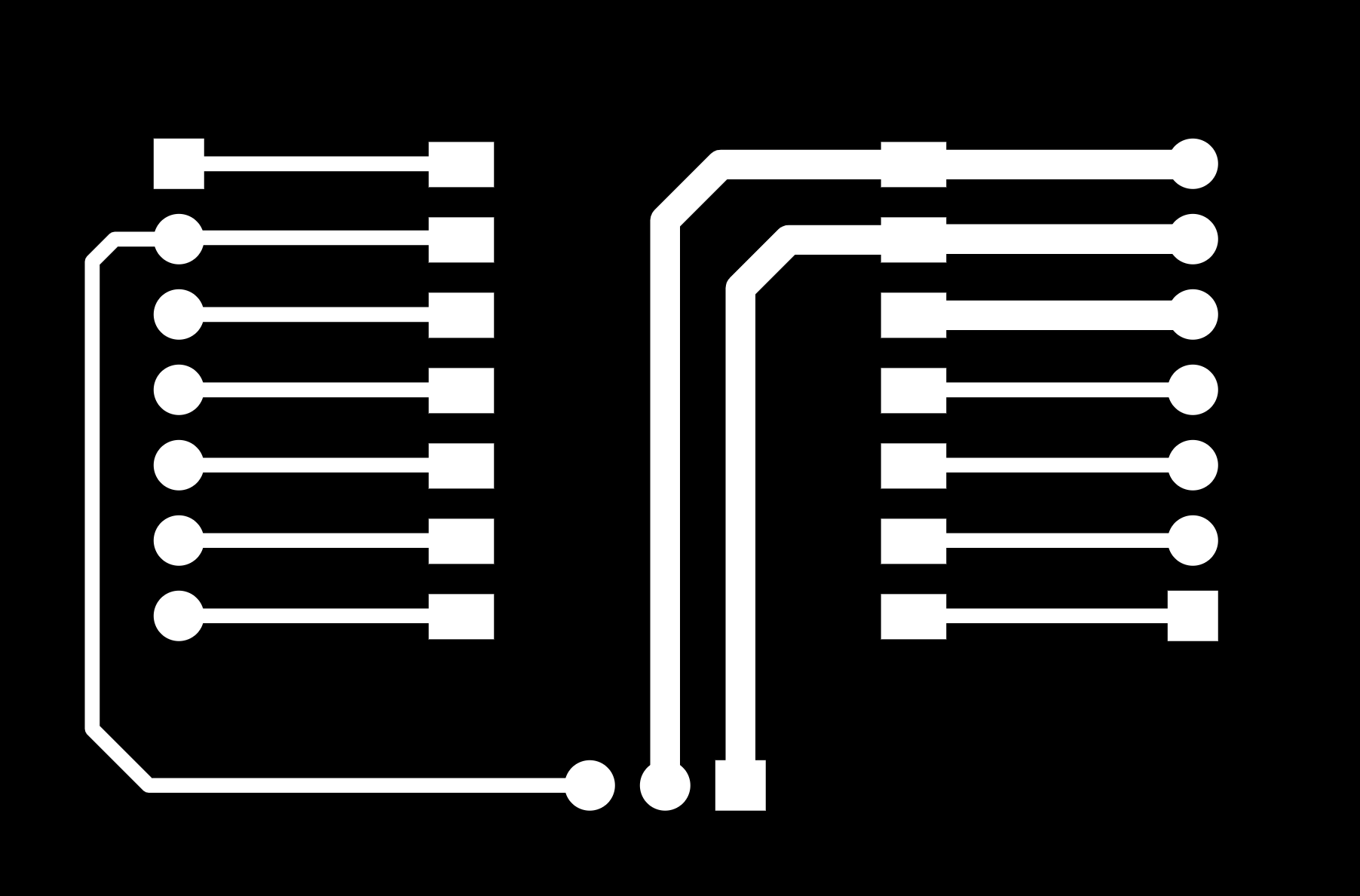
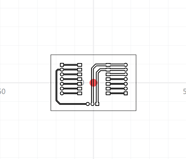
I exported the cutout and drilling images.

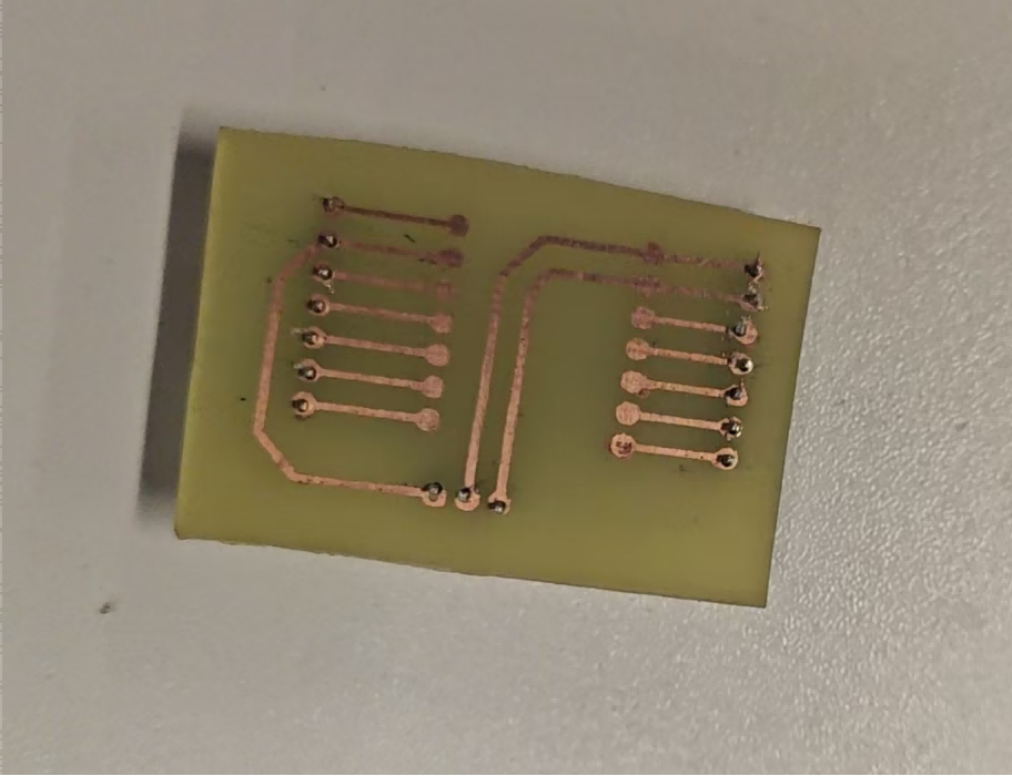
Since the CNC machine I was using this week broke down, I decided to try one of the most traditional methods—chemical etching—to make my own PCB. Although this process is more cumbersome than mechanical machining and involves chemical handling, the overall experience was rewarding and helped me better understand the fundamental principles of PCB formation.
What is the etching method?
The etching method is a technique that removes excess copper from a copper-clad board using an etching solution. Simply put, it involves protecting the parts of the circuit you want to keep (for example, using toner or oil-based ink), and then using the etching solution to "bite away" the unwanted copper. In the end, only the conductive traces of the circuit pattern remain.
Materials and Tools Used
| Item | Description |
|---|---|
| Single-sided copper-clad board | Common phenolic board or fiberglass board |
| Laser printer | Used to print the circuit pattern (inkjet printers do not work) |
| Glossy paper / transfer paper | Used for transferring the pattern (I used magazine paper) |
| Iron / laminator | Used to heat-transfer the pattern |
| Ferric chloride (FeCl₃) | Commonly used etching solution |
| Plastic container | For holding the etching solution (metal containers are not allowed) |
| Gloves, mask | Basic protection during chemical handling |
| Alcohol / nail polish remover | For cleaning the board and removing toner |
| Electric drill / manual drilling tool | For drilling component holes |
Detailed Production Steps
Detailed Production Steps
- I exported the PCB layout as a mirrored image, because the heat transfer process is reversed.
- Surface Cleaning
I gently sanded the surface of the copper-clad board with fine sandpaper to remove the oxidation layer. Then I wiped it clean with alcohol to ensure it was free of oil and dust. - Pattern Transfer
I placed the printed pattern tightly against the copper board, soaked it in water for a few minutes, and then carefully peeled off the paper. The toner pattern remained on the board.
For any areas that didn’t transfer well, I manually filled them in with a black oil-based marker. - PCB Etching
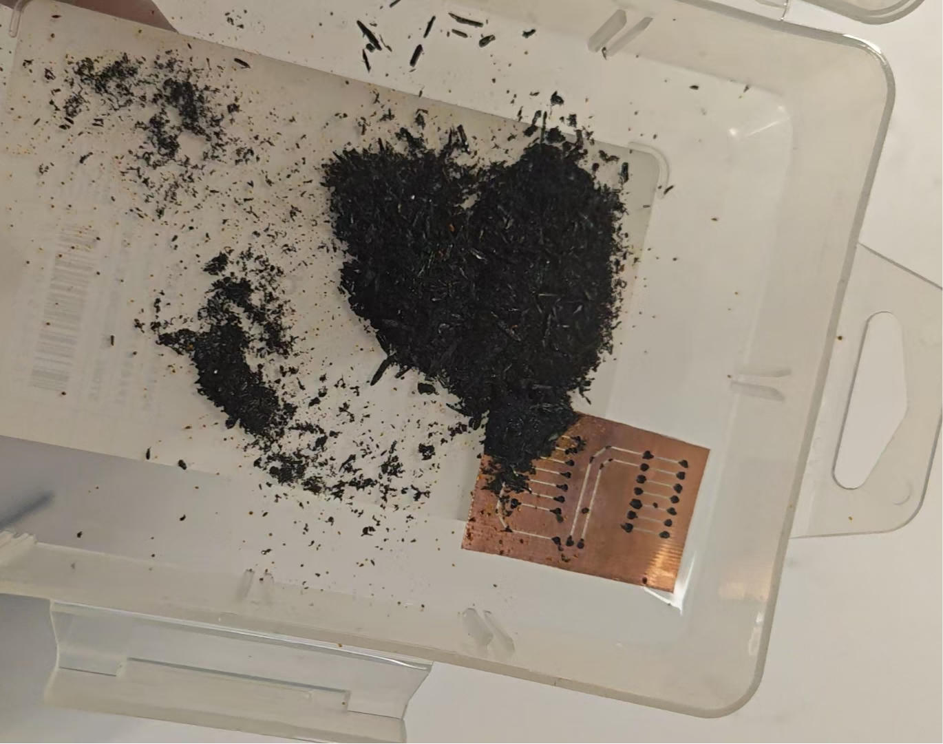
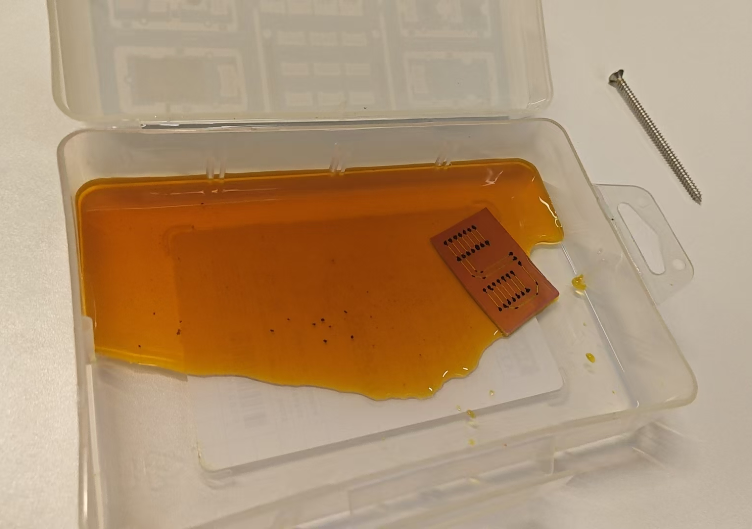
I poured ferric chloride solution into a plastic container, warmed it slightly, and placed the board inside. I gently shook the container to help the etching proceed evenly. After about 20 minutes, the exposed copper was completely etched away, leaving only the desired pattern.
⚠️ I wore gloves and a mask throughout the process and worked in a well-ventilated area to ensure safety. - Cleaning and Refinement
I rinsed the board thoroughly with water, then used nail polish remover to wipe off the toner and reveal clear copper traces. - Drilling and Soldering Preparation
Finally, I used an electric drill to make component holes. After cleaning up the burrs, the PCB was ready for soldering!
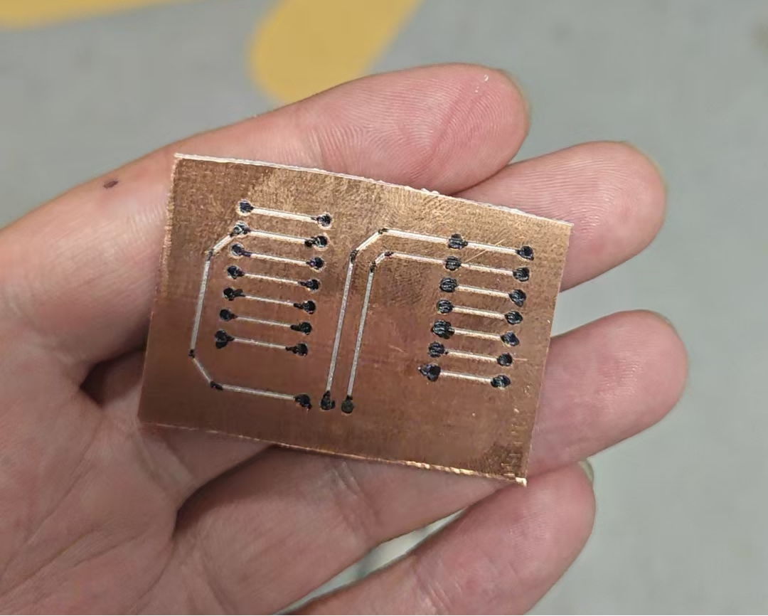
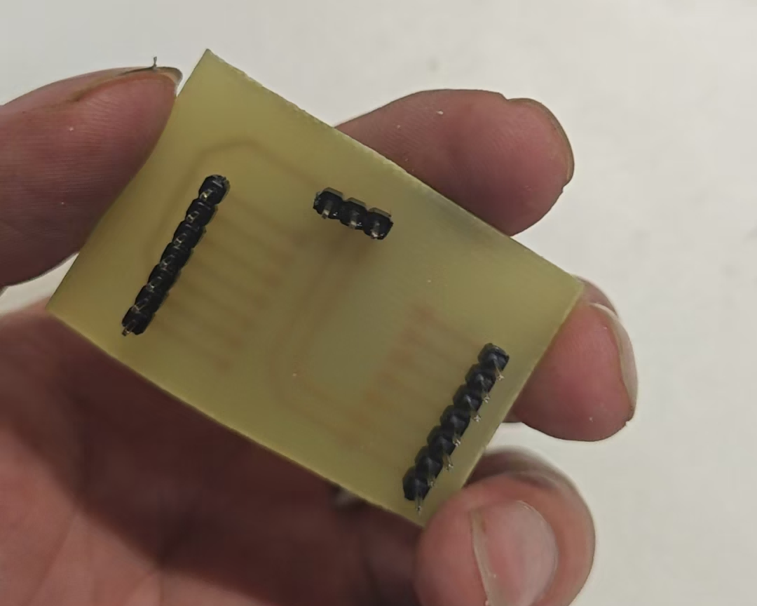
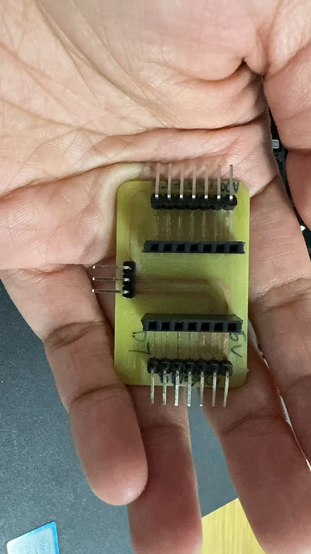
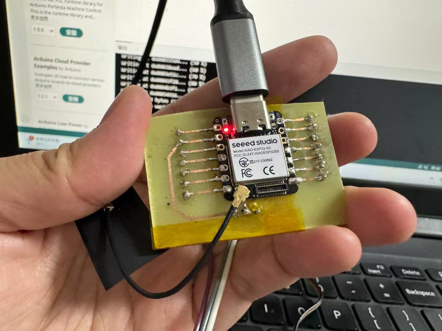
After applying a solder mask sticker, I proceeded with soldering. I soldered the ESP32S3 main board onto the extension board.
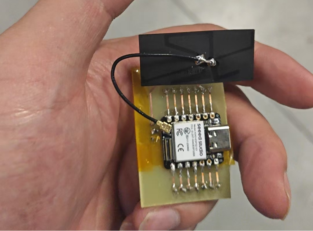
Test: LED Blinking Program Verification
After completing the PCB etching process, I continued with functional testing of the output device. This time, I chose a single-color LED module and used simple programming to make it blink, in order to verify whether the output pin on the extension board was functioning correctly.
Wiring Instructions
The LED module I used comes with a built-in current-limiting resistor, so it can be connected directly to the development board without an external resistor. The module lights up with a HIGH signal.
| LED Module Pin | Connection |
|---|---|
| VCC | 3.3V |
| GND | GND |
| Signal | GPIO2 (D2) |
Arduino Code
I wrote the following simple code in Arduino IDE to make the LED blink in a 0.5-second cycle:
#define XIAO_ESP32S3_D1
                #define LED_PIN 3  // Connected to D2

                void setup() {
                  pinMode(LED_PIN, OUTPUT);
                  digitalWrite(LED_PIN, HIGH);  // Turn on the LED
                }

                void loop() {
                  digitalWrite(LED_PIN, HIGH);
                  delay(500);
                  digitalWrite(LED_PIN, LOW);
                  delay(500);
                }
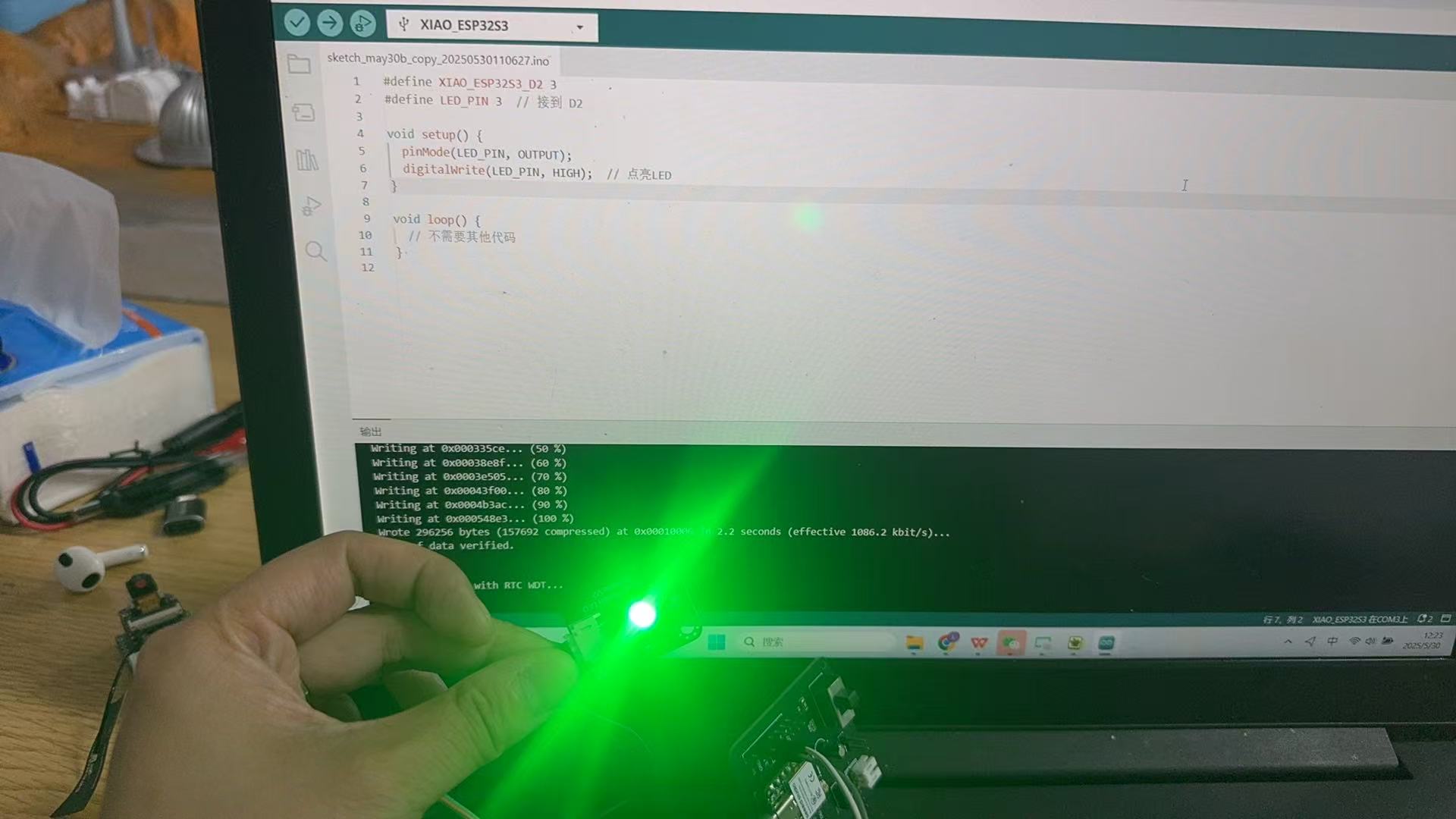
Testing Process and Results
After uploading the code, the LED module started blinking as expected.
I tried modifying the delay() values to observe changes in the blinking rhythm.
At the same time, I confirmed that the D2 pin on the extension board was outputting the correct logic level.
There was no heat or abnormality from the power wiring or the module, indicating that the current-limiting design worked well.
Through this small test, I verified the following:
- The custom-made PCB extension board had reliable connections, and the D2 pin functioned correctly.
- The LED module responded well, and the program logic produced the expected output.
- I gained a deeper understanding of digital output control (HIGH → ON, LOW → OFF).
- This was also the first successful "power-on" test after completing the entire circuit board, which made it especially meaningful!
Process Record of Using Snapmaker CNC to Mill a FR4 Copper-Clad PCB
1. Materials and Tools Preparation
| Item | Description |
|---|---|
| Material | Single-sided FR4 copper-clad board |
| Tool | PCB engraving bit |
| Equipment | Snapmaker 2.0 with CNC module |
| Software | Snapmaker Luban |
| Mounting | Fix the PCB with double-sided tape or clamps |
2. File Design and Preparation
1. Circuit Design and Export
Export the top layer routing diagram as a DXF file:
- The DXF file should retain only the trace outlines (used for engraving paths).
2. Upload DXF to Snapmaker Luban
- Open Snapmaker Luban and select the CNC function.
- Click “Import” > upload the DXF file.
- Choose the appropriate engraving surface size and align the design to the center of the workspace.
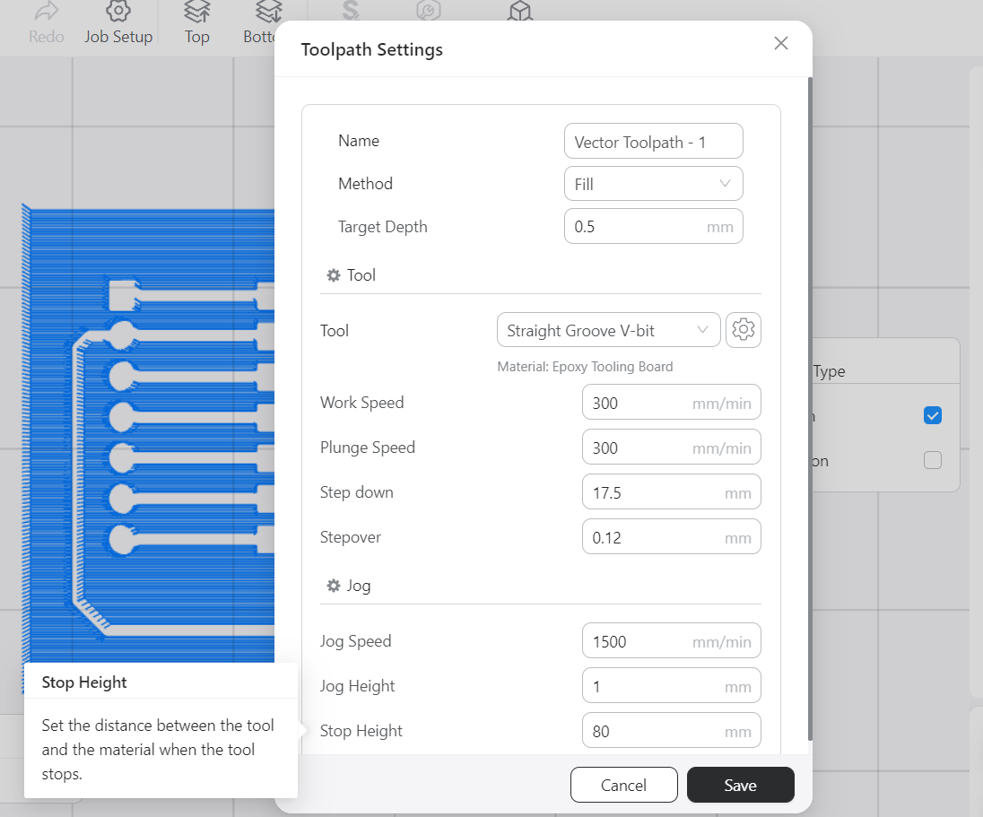
3. Toolpath Setup
1. Set Tool Parameters
In Snapmaker Luban:
- Select tool type: V-Bit (tapered engraving bit)
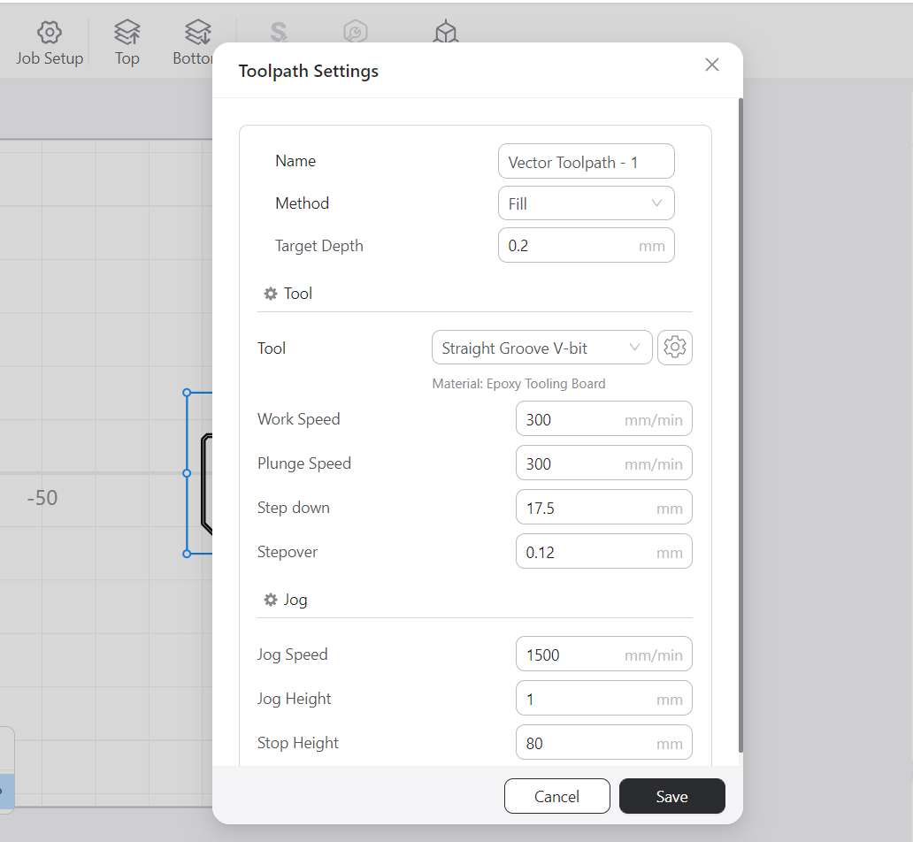
2. Generate Toolpath
Under “Create Toolpath”, configure relevant parameters.
3. Export G-code
After setup, click “Generate G-code” and save the file to a USB drive.
4. Machine Setup and Engraving Process
1. Install the Tool and Secure the Material
- Install the engraving bit and tighten it with the provided wrench.
- Use clamps to firmly fix the PCB board onto the CNC platform.
2. Set Origin (X/Y/Z)
On the touchscreen, use "Manual Control":
- Move the bit tip to the center of the PCB and set it as the XY origin.
- Lower the Z-axis until the bit just touches the copper surface and set it as the Z origin.
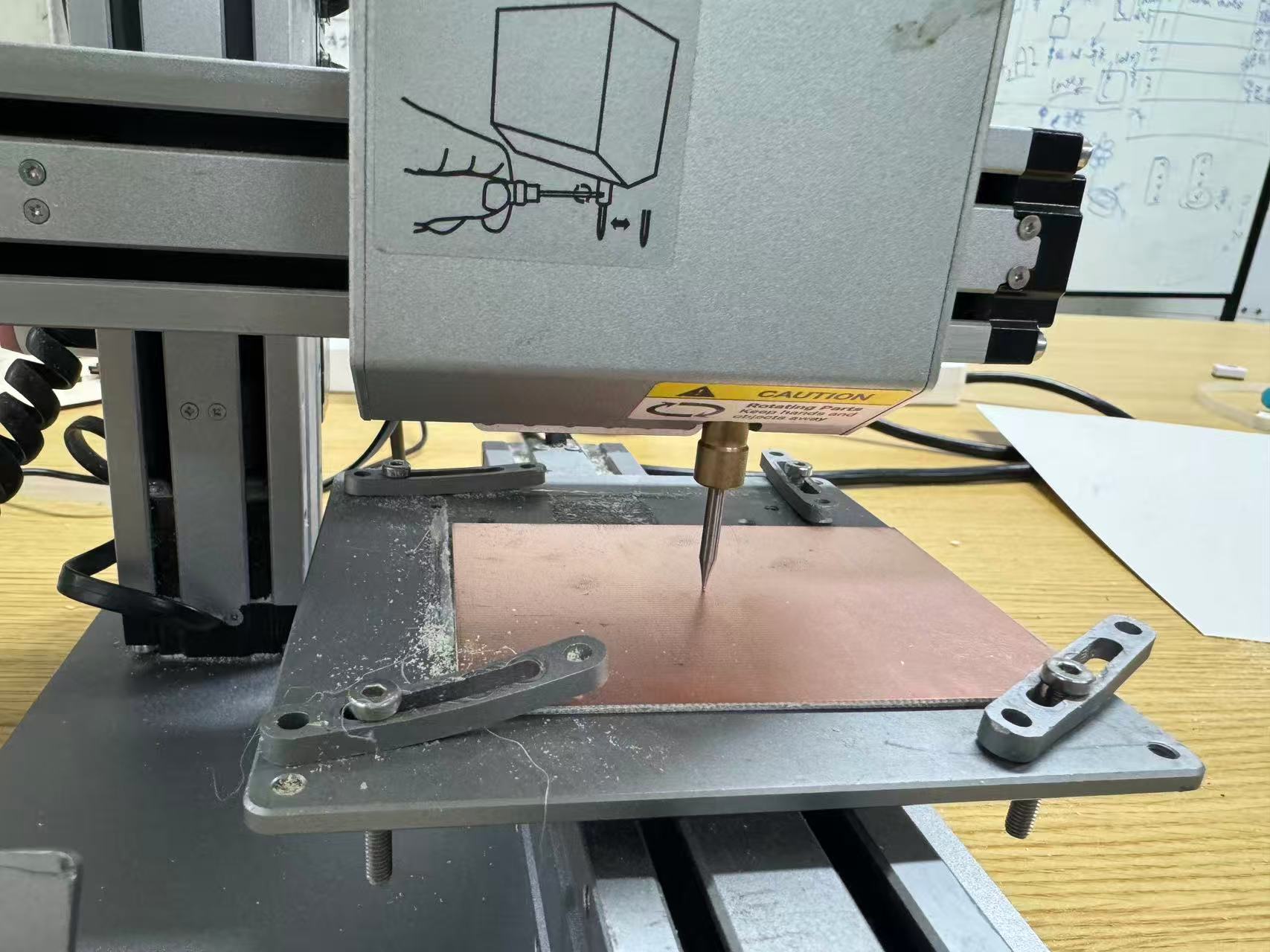
3. Start Engraving
- Select the corresponding G-code file to start engraving.
- Keep an eye on the process to ensure the bit does not shift or loosen.
5. Post-Processing After Engraving
1. Clean Debris
Use a brush to remove dust.
2. Check the Circuit
Use a multimeter to test circuit continuity.
3. Drilling and Soldering
The PCB has through-holes; I manually drilled them and soldered the components.