Electronics Design
Back to HomeGoals
Group assignment:
- use the test equipment in your lab to observe the operation of a microcontroller circuit board
Individual Assignment
- use an EDA tool to design and check a development board that uses parts from the inventory to interact and communicate with an embedded microcontroller
- extra credit: try another design workflow
- extra credit: simulate your design
- extra credit: design a case around your design
Group Assignment
Project Background
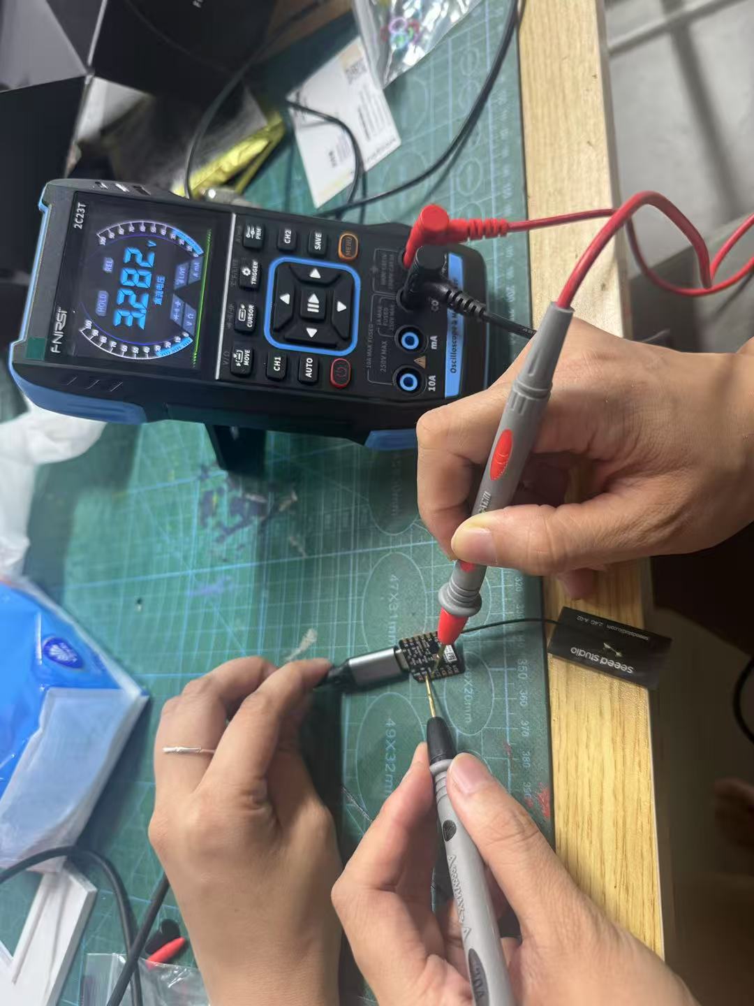
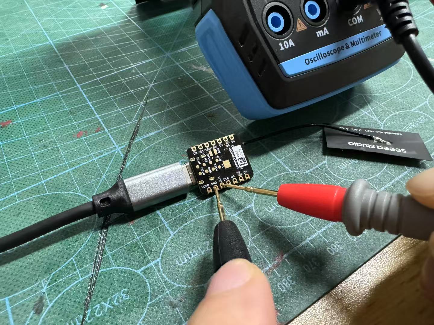
As part of this week's electronics design assignment, our group used lab equipment to observe and analyze the behavior of a Seeed XIAO ESP32 development board. This task helped us understand power, signal, PWM, and UART communication in real conditions, preparing us for our own board design.
Equipment Used
- Digital Multimeter – to measure voltage and logic levels
- Oscilloscope – to visualize PWM and switching signals
- ArduinoIDE
Testing Procedures and Results
1️⃣ Power Test (Multimeter)
We verified the 3.3V output from the VCC pin.
2️⃣ PWM Signal Observation (Oscilloscope)
The uploaded code on the XIAO is designed to make the LED connected to D9 fade in and out.As a result, we can observe on the oscilloscope that the waveform's duty cycle is continuously changing.
                    /* Fade example for Arduino */
                    int led = 9;
                    int brightness = 0;
                    int fadeAmount = 5;

                    void setup() {
                      pinMode(led, OUTPUT);
                    }

                    void loop() {
                      analogWrite(led, brightness);
                      brightness = brightness + fadeAmount;

                      if (brightness <= 0 || brightness >= 255) {
                        fadeAmount = -fadeAmount;
                      }

                      delay(30);
                    }
Individual Assignment
Project Background
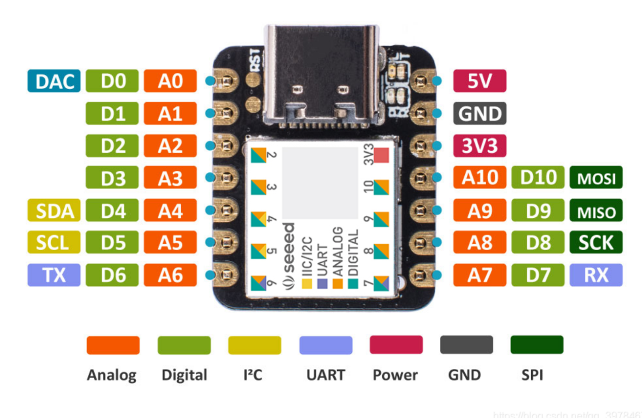
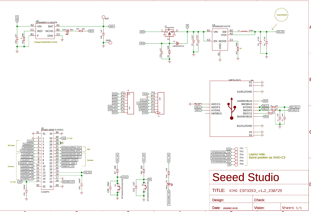
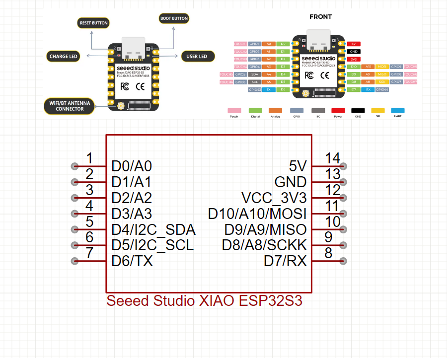
This is one of my assignments for Fab Academy — to use PCB design tools to create a functional circuit board. I chose to design an extension board for the Seeed Studio XIAO ESP32-S3 microcontroller, with the goal of making this compact board easier to connect with external devices.
Before getting started, I reviewed the official hardware documentation of the XIAO ESP32-S3 to understand its pin layout, power requirements, and interface limitations. This research was very helpful for the design work that followed.
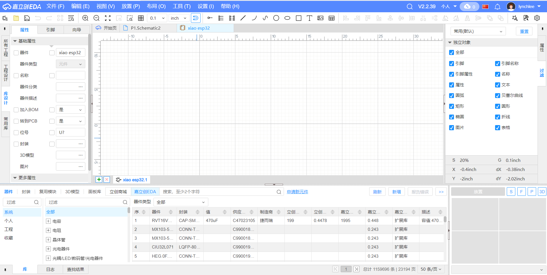
Schematic Design (Using JLCEDA)
Tool Overview: JLCEDA
JLCEDA is one of the most widely used online PCB design tools in China, developed by JLCPCB. It is completely free and provides the following features:
- Schematic design
- PCB layout
- Component library management
- One-click Gerber file generation
- Seamless integration with JLCPCB's fabrication service
I chose JLCEDA because of its clean interface and intuitive operations, which make it suitable for both beginners and advanced users.
One feature I particularly appreciate is that JLCEDA is tightly integrated with the JLCPCB manufacturing service, which offers two free PCB orders per month for boards up to 100mm × 100mm. This is especially student-friendly.
Official JLCPCB website: https://www.jlc.com/?from=PZ-pLpu&s=JC

Create the Schematic Project
First, I downloaded the JLCEDA Order Assistant for PC from the official site: https://www.jlc.com/portal/appDownloadsWithConfig.html?spm=PCB.Homepage.functionbar.1022 and registered an account.
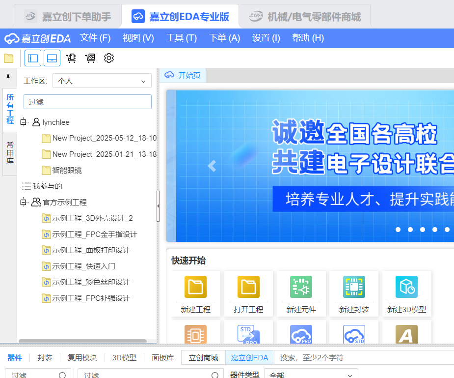
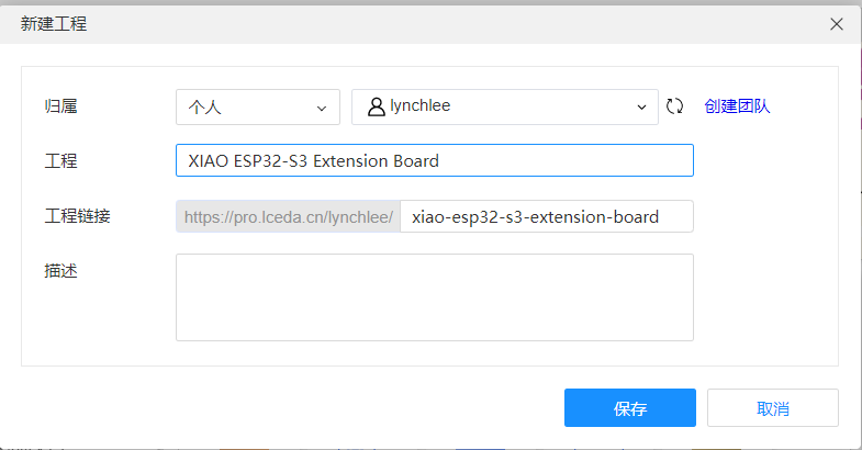
Then I opened the EDA Pro version. On the Quick Start page, I clicked "New Project" → "Schematic + PCB Project".
I named the project "XIAO ESP32-S3 Extension Board" and used the default settings.
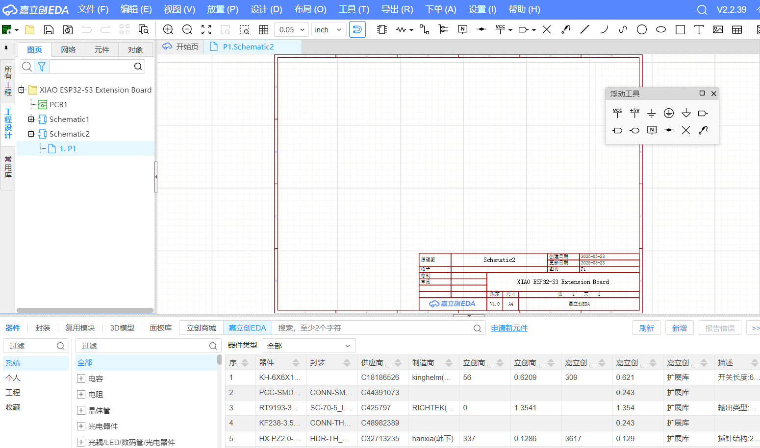
After creating the project, it automatically entered the schematic editor interface.
Design Plan
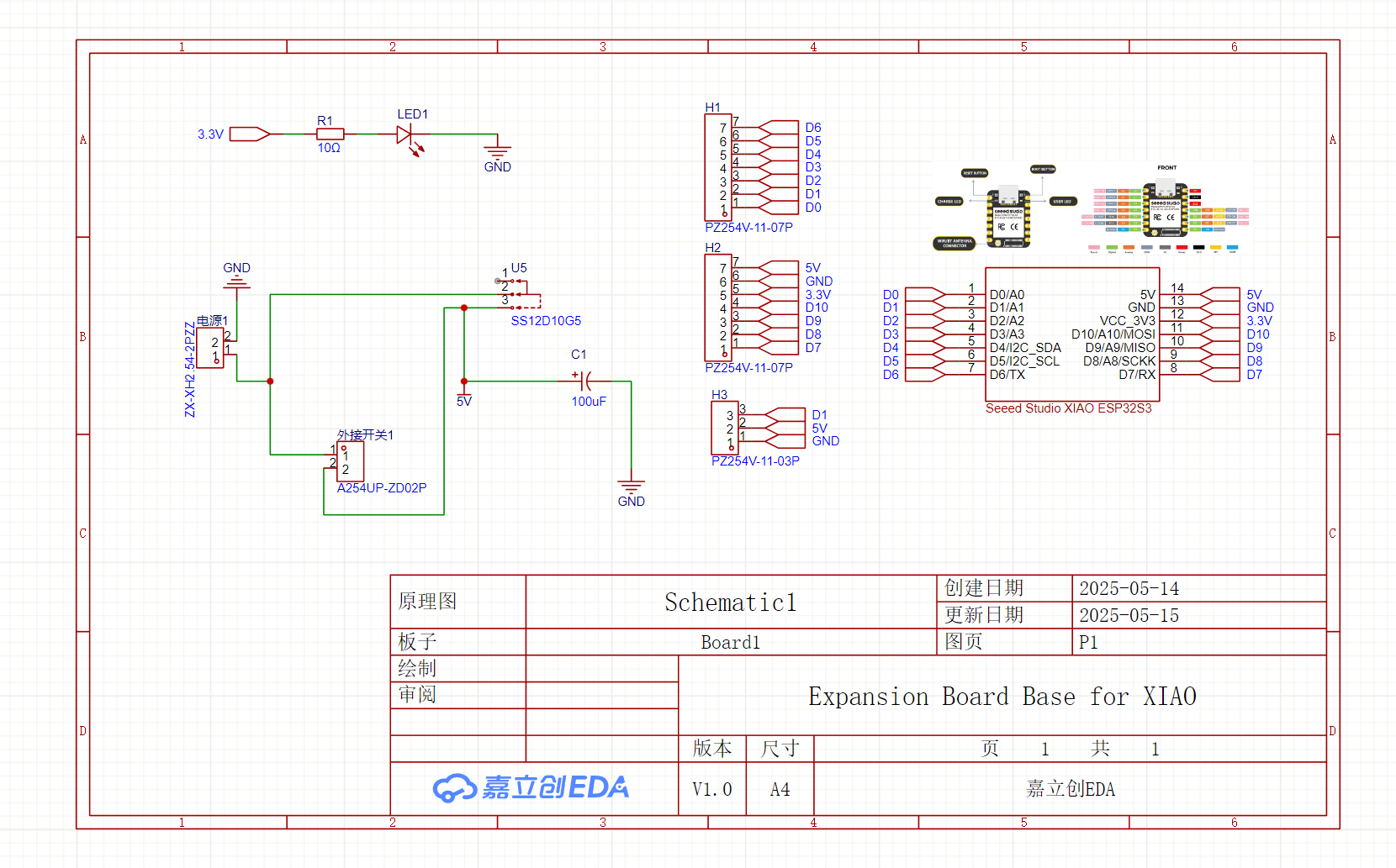
In this step, I used JLCEDA to draw the schematic for the extension board. Right from the beginning, I decided to include the following four major functional modules:
- An external push-button input
- A servo motor control interface
- GPIO pin breakout headers
- One additional GPIO expansion pin
Manually Creating the XIAO ESP32-S3 Component
This was the most time-consuming but also the most rewarding part of my entire design process.
Creating the Symbol
I clicked the top menu "My Components" → "New Component" to start building the symbol manually.
I named the component "XIAO ESP32-S3". The core pins I included are:
- 3.3V power input
- GND
- Common GPIOs (e.g., D1, D2, D3, D4)
- I2C: SDA, SCL
- UART: TX, RX
I drew all these pins as a dual-row header (2x7) in the schematic symbol editor to match the physical layout for breakout purposes.
In the symbol editor, I manually added 14 pins arranged in two vertical columns:
- Left side: D0, D1, D2, D3, 3V3, GND, RST
- Right side: TX, RX, SDA, SCL, D4, D5, 5V
Each pin was configured with its correct electrical type (e.g., Power, Input, Bidirectional, etc.), aligned neatly, and labeled accordingly.
After confirming the layout and checking for consistency, I saved the symbol to be used in the schematic.
Key Circuit Modules in the Schematic
External Push-Button Circuit
I used a simple push-button connected to a GPIO pin along with a 10kΩ pull-up resistor:
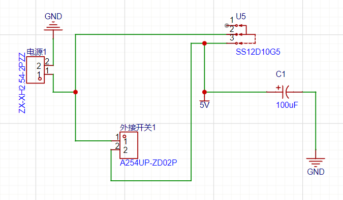
            GPIO → Button → GND
                ↘ 10kΩ ↗
                3.3V
The pull-up resistor prevents the GPIO pin from floating when the button is not pressed. In the code, I configured the pin as input with pull-down mode to detect HIGH and LOW transitions reliably.
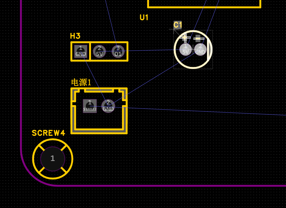
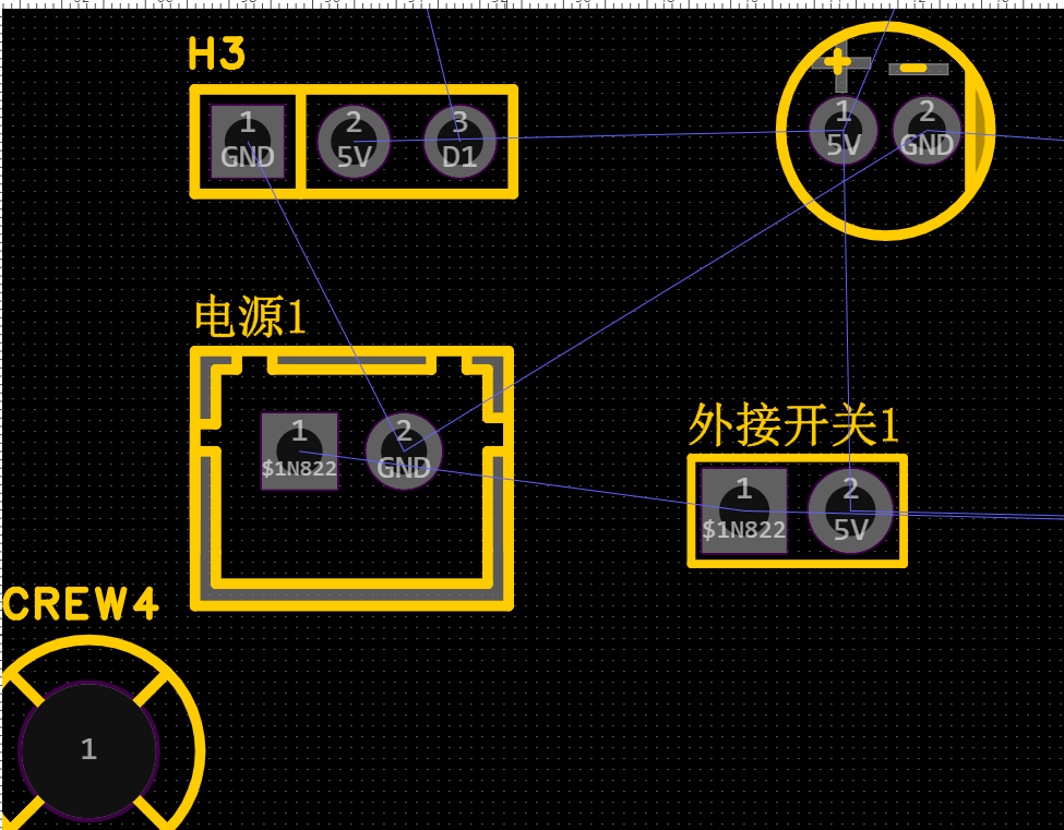
Servo Motor Control Interface
Servo motors usually operate at 5V, so I created a dedicated 3-pin header (VCC, GND, PWM) for the servo:
- The PWM signal pin is connected to D3 (or another PWM-capable GPIO)
- VCC is sourced directly from the XIAO ESP32-S3's 5V USB input
- GND is shared with the board's ground
To suppress electrical noise and provide power stability, I added two capacitors between VCC and GND:
- A 100μF electrolytic capacitor for bulk filtering
- A 0.1μF ceramic capacitor in parallel for high-frequency decoupling
These three connections are output through a standard 3-pin servo header on the PCB.
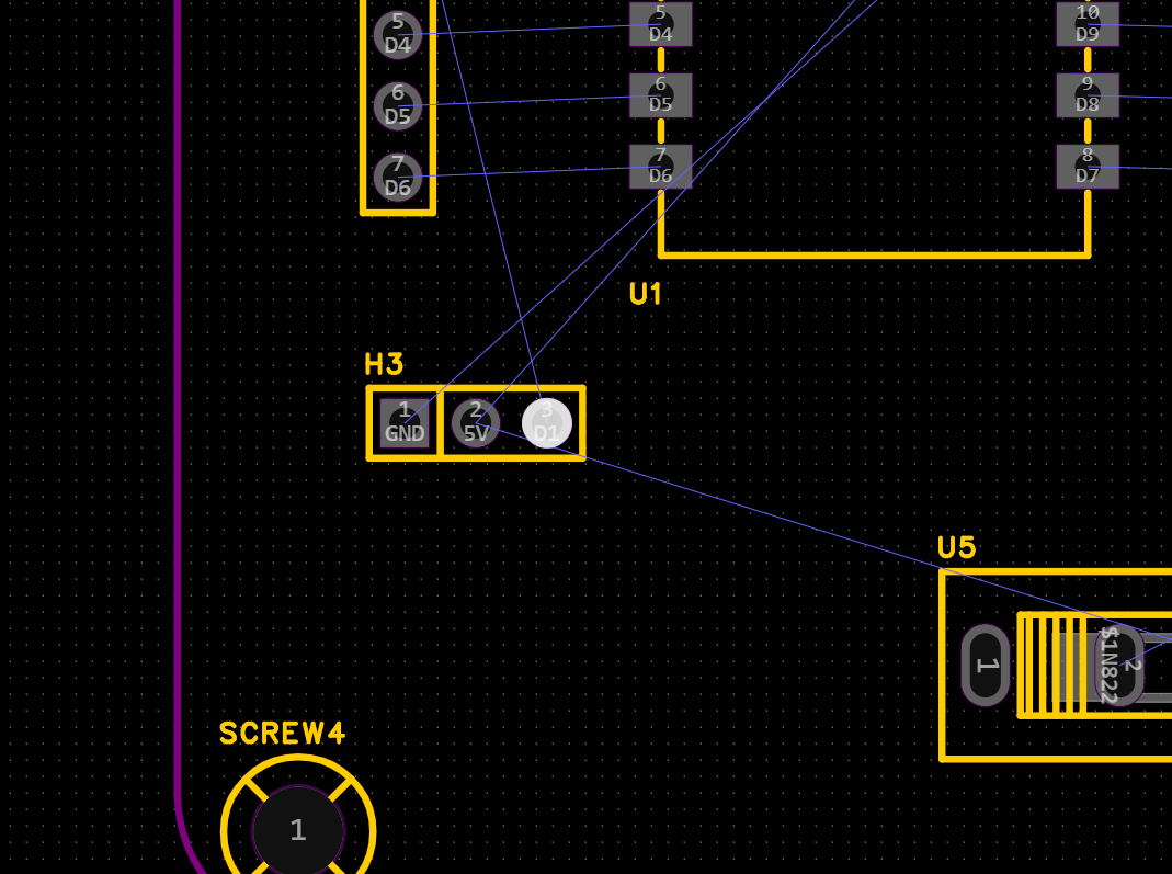
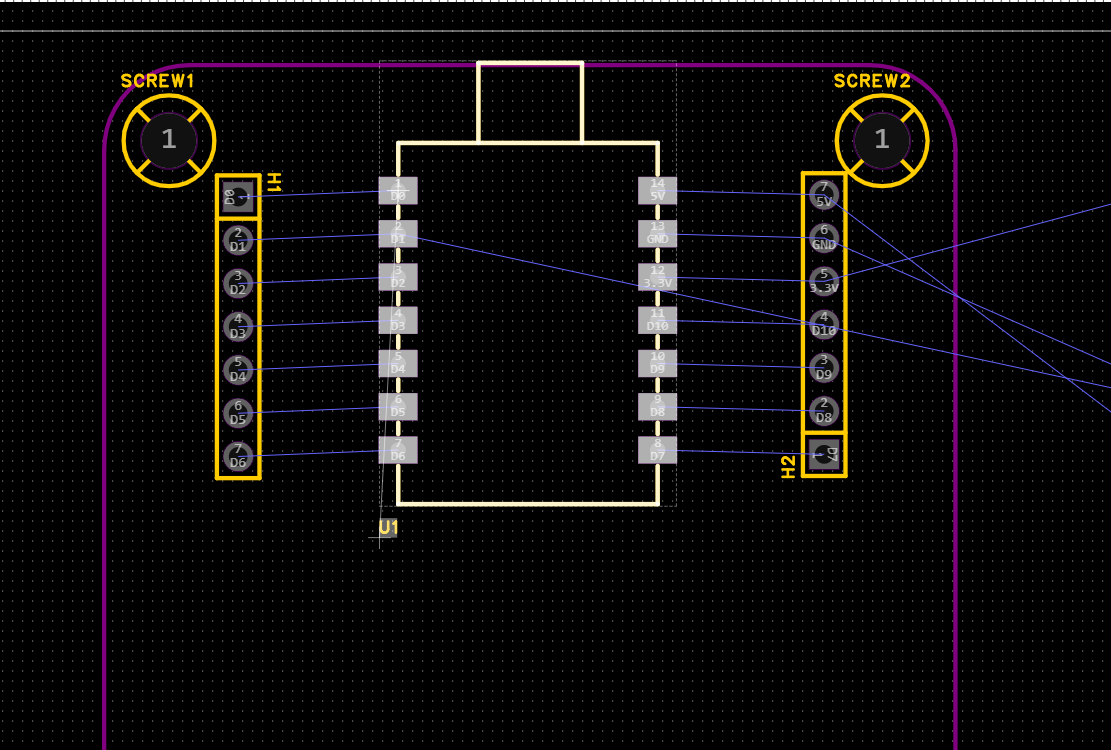
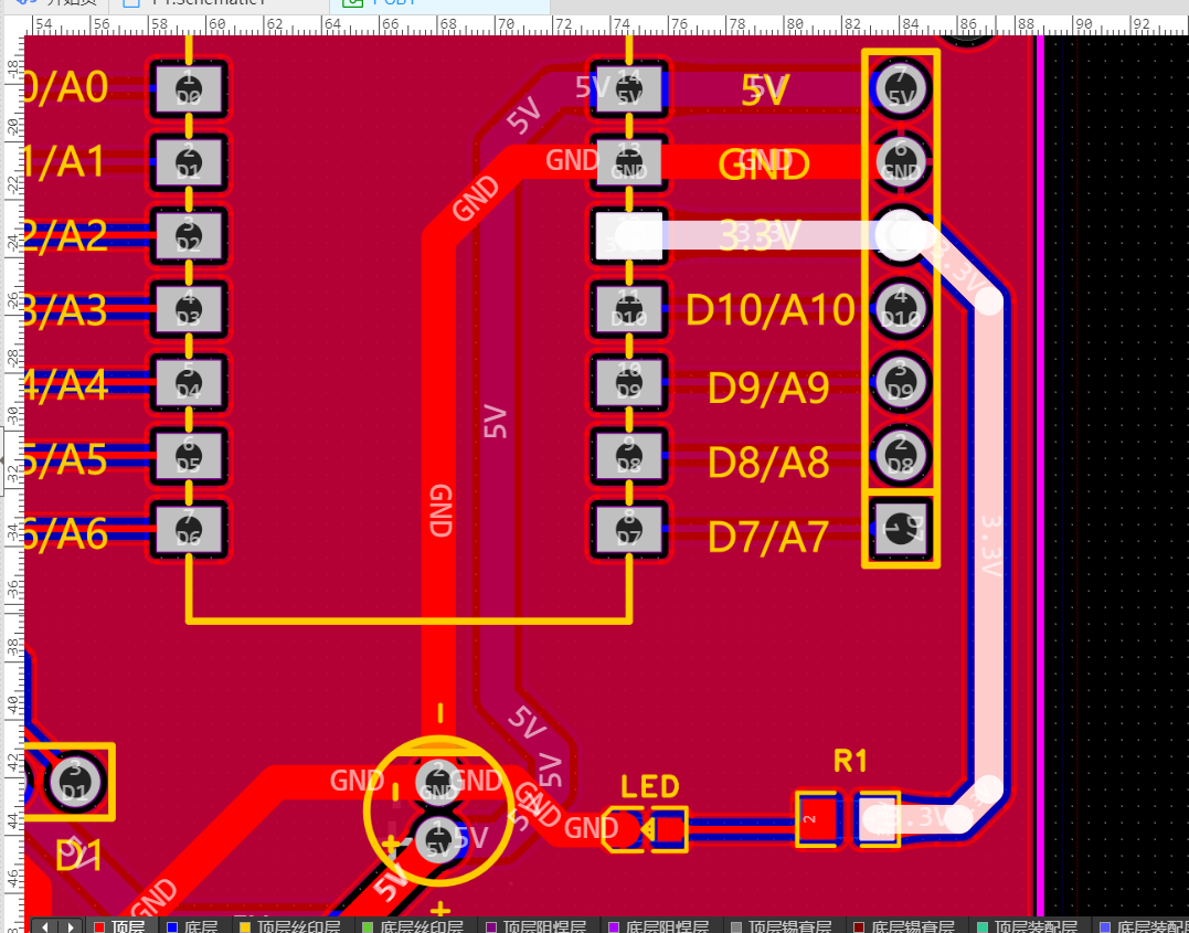
GPIO Pin Breakout
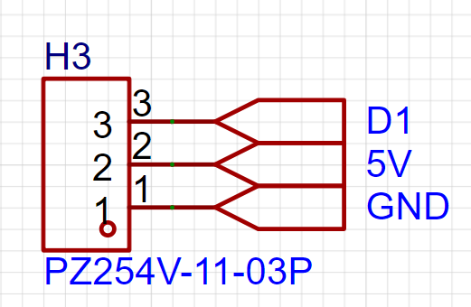
I broke out several unused GPIO pins from the microcontroller (such as D4, D5, TX, RX) to a pin header.
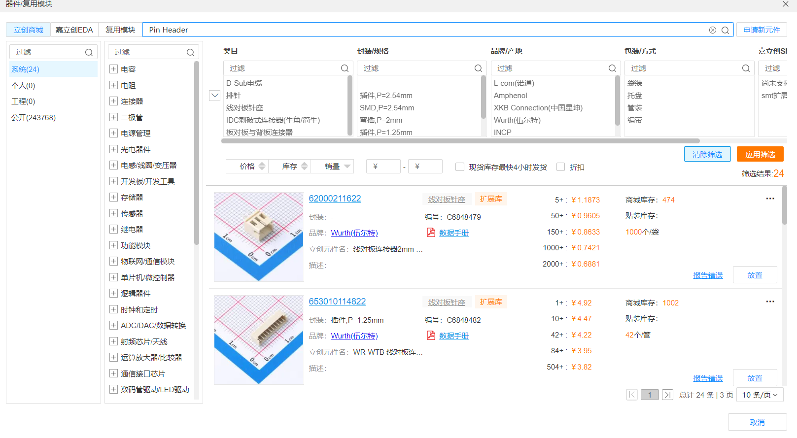
- I searched for the Pin Header component in the library and selected a 1x7 header
- I connected each GPIO to a separate pin on the header using wires in the schematic
- I labeled each pin with its corresponding function and name in the schematic
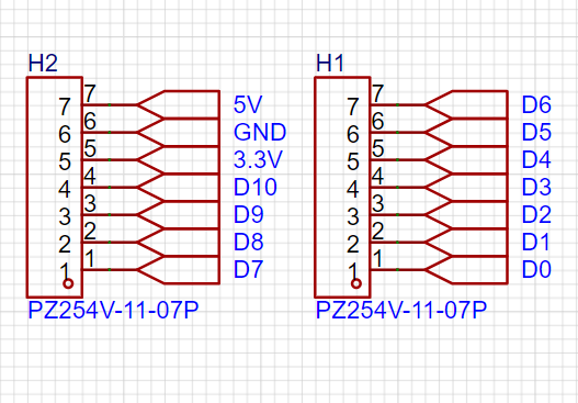
These labels will also be printed as silkscreen on the PCB surface to make it easier to identify pins during use.
The breakout header makes it convenient to connect LEDs, sensors, serial modules, or other external components.
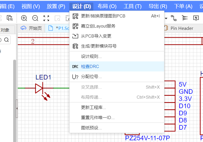
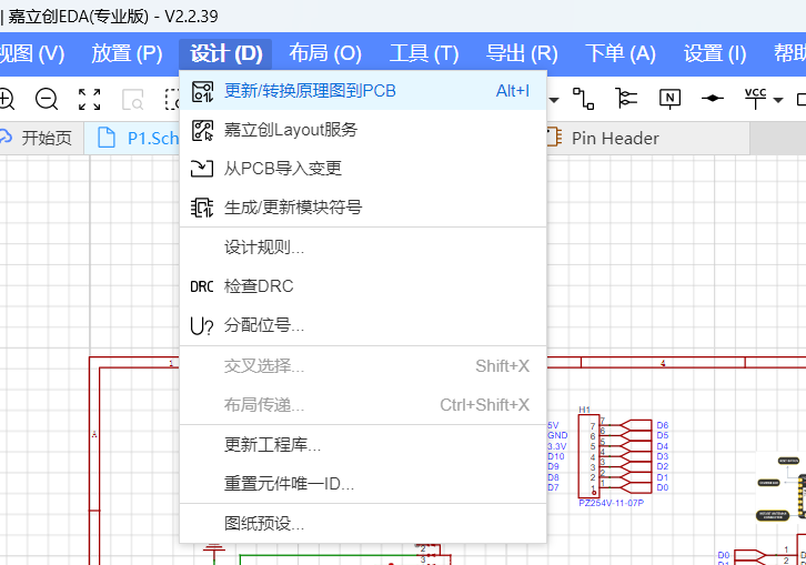
ERC Check (Electrical Rule Check)
After connecting all the wires in the schematic, I clicked "Design" → "ERC Check" in the top menu of JLCEDA. This step is crucial to make sure there are no "fatal errors" in the circuit design.
The system automatically scans for common issues like unconnected pins, short circuits, or missing power connections.
If there’s a warning, I simply click on the red icon and the software jumps directly to the problematic area — super convenient!
Once all the red warnings disappeared, I knew that my schematic was logically sound and ready to move on to the PCB layout stage!
PCB Layout Design
After completing the schematic, I moved on to the PCB layout stage using JLCEDA’s PCB editor. This part took me quite some time to fine-tune, because I had to consider not only the correctness of the electrical connections, but also the aesthetics, compactness, solderability, and usability of the final board.
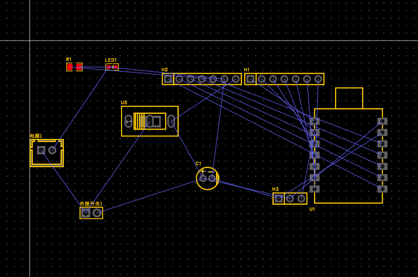
To start, I clicked "Design" → "Convert Schematic to PCB" from the top menu in JLCEDA.
To be honest, I was a bit overwhelmed at first.
All the components were automatically scattered across the canvas, and the screen was filled with a web of blue "air wires" (also called ratsnest lines). The connections looked like a tangled mess — I couldn’t tell what was going where at all. It felt like someone had dumped a whole bowl of spaghetti on the screen.
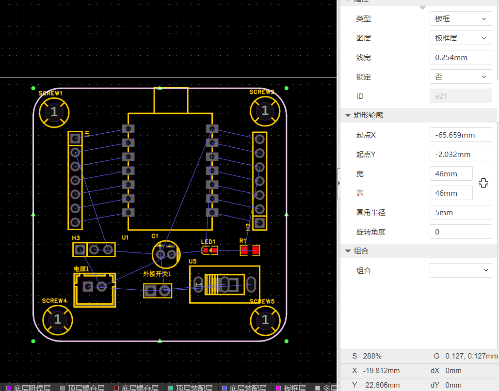
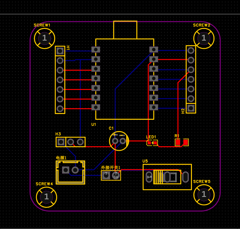
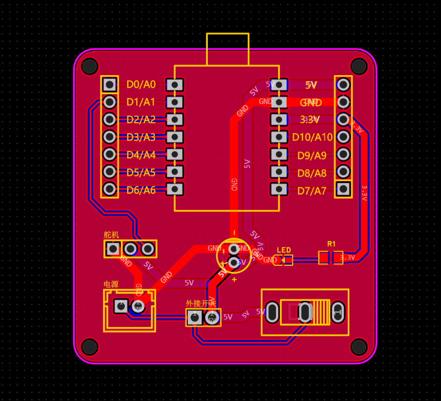
Drawing the Board Outline and Setting Dimensions
I started by drawing a rectangular outline along the edge of the canvas to define the shape of the board.
I set the size to 50mm × 50mm, which I estimated based on the number of components I needed to place.
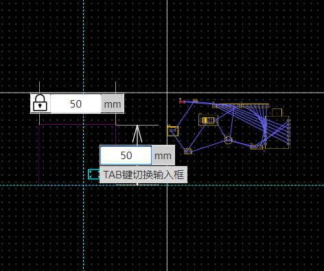
I personally think that rounded corners make the PCB look nicer, so I set a 5mm corner radius in the board outline properties.
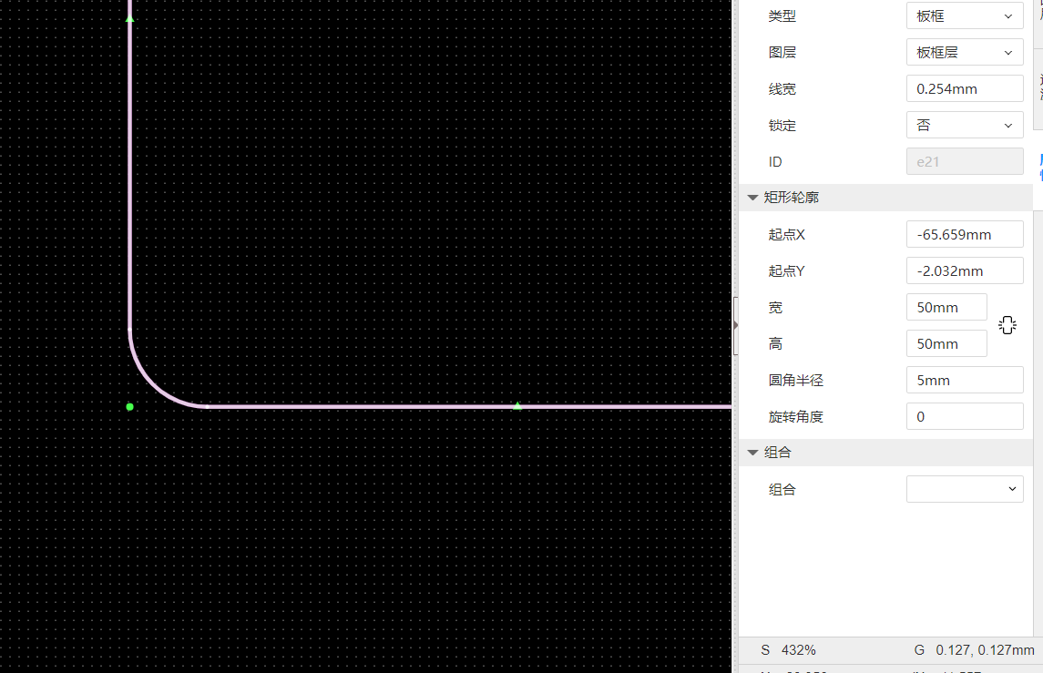
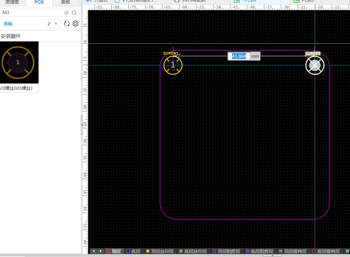
Next, I added four mounting holes — each with a diameter of 3mm — at the corners of the board. These will allow me to fix the board into a case or chassis later on.
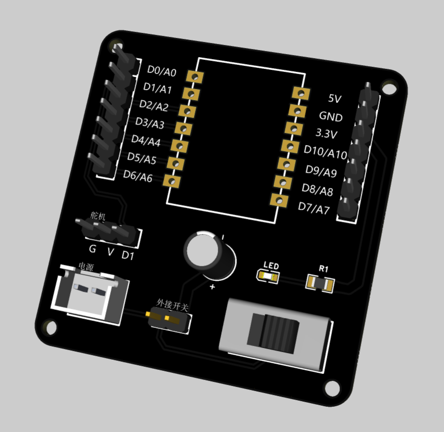
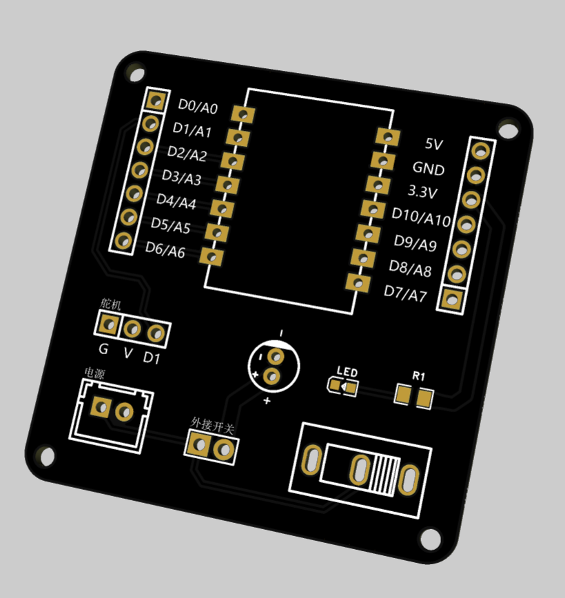
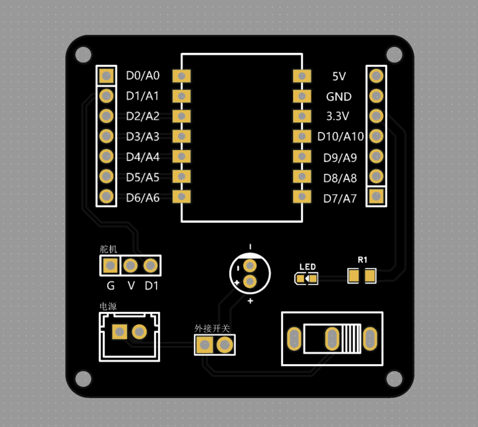
Most importantly, I fixed the position of the XIAO ESP32-S3’s pin headers right away, because they form the core of the entire expansion board layout.
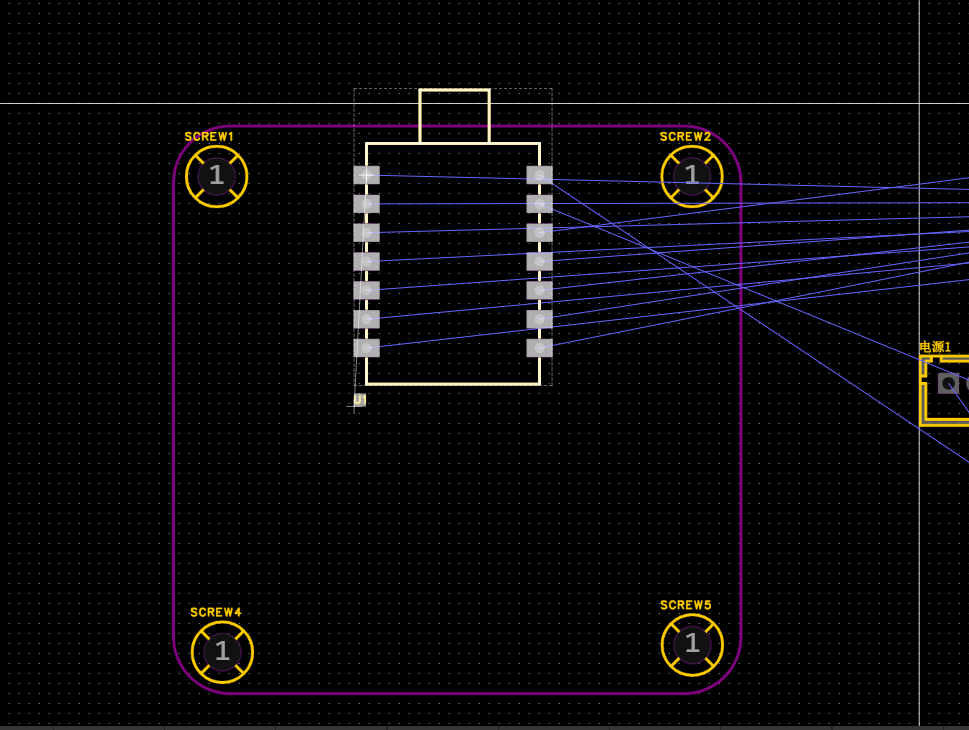
Component Placement Strategy
For the layout, I followed a strategy of “functional zoning first, then compact adjustment.”
- Main XIAO header pins: Placed along the sides of the board, aligned and close to the edges to make plugging and unplugging easier.
-
Servo interface: Positioned in the bottom-left corner, with a clearly labeled 3-pin connector (PWM / 5V / GND).
The PWM signal trace is kept short, and the 5V supply is routed from the USB input.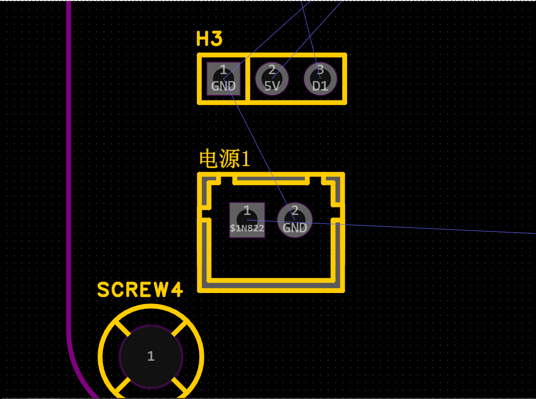
- Decoupling capacitors: A large 100μF electrolytic capacitor and a 0.1μF ceramic capacitor are placed near the servo connector.
- Button module: Also located in the bottom-left area of the board, with a hole reserved in the outline so the button can be easily accessed.
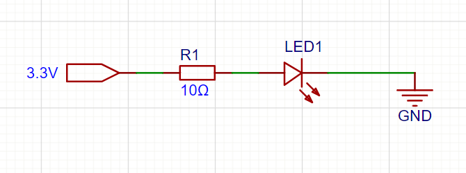
- Power indicator LED: Positioned near the bottom center of the board. It's a surface-mounted LED with a series current-limiting resistor.
- Extra GPIO breakout: Placed directly below the LED, allowing for easy access to additional I/O pins.
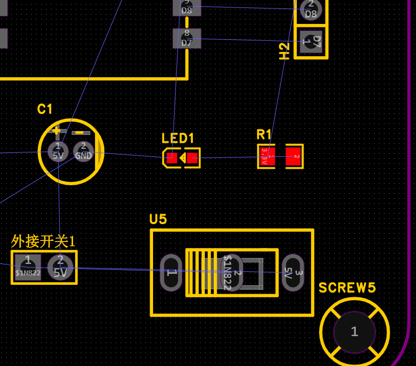
After placing all the components, I felt the board outline was a bit too large, so I resized it down to 46mm × 46mm to make the layout more compact.
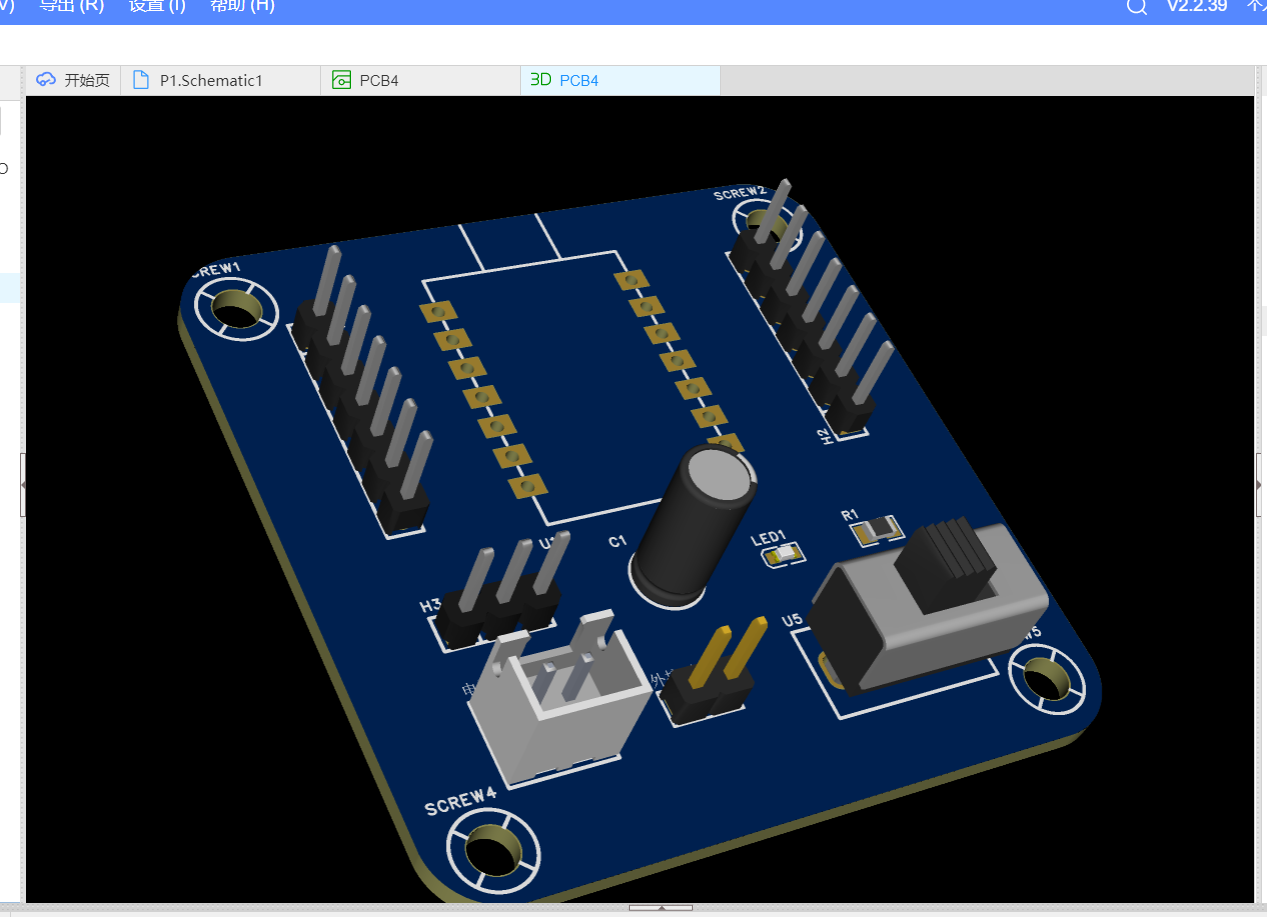
After arranging all the components, I clicked the "3D" button in the toolbar to preview the board in 3D.
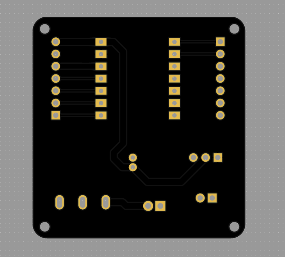
I used the auto-routing feature to automatically connect all the nets on the PCB.
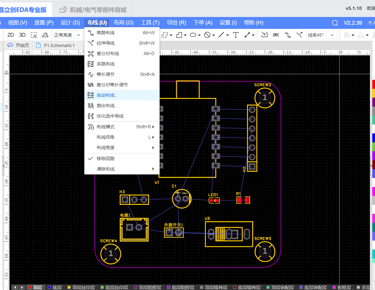
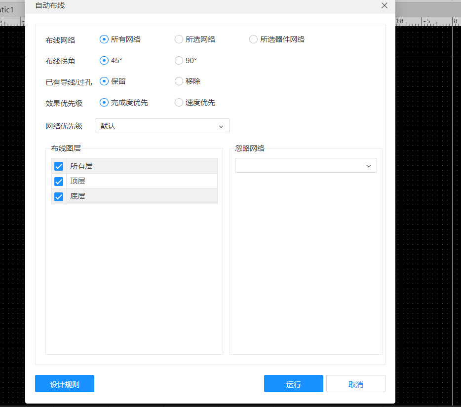
After completing the auto-routing, I made several manual adjustments based on standard routing principles to improve performance and reliability:
Power Traces (3.3V, 5V)
- I used 0.8mm wide copper traces to ensure sufficient current capacity.
- The 5V trace going to the servo header was made especially wide and routed with minimal turns to reduce voltage drop and noise.
Ground Plane
- I poured GND copper on both top and bottom layers to enhance grounding and signal integrity.
- To further reduce impedance, I added multiple vias to connect the top and bottom GND planes.
Signal Traces
- I kept all digital signal lines short and straight to minimize resistance and potential interference.
- I maintained tight and parallel routing for I2C and UART signals to ensure clean communication paths.
Vias and Layer Switching
- I used standard 0.6mm vias to connect traces between the top and bottom layers.
- In cases where traces needed to cross power lines, I used vias to reroute them on the opposite layer to avoid interference.
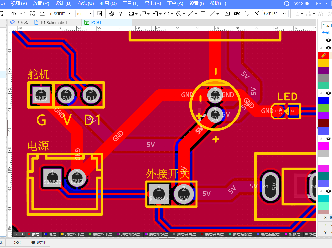
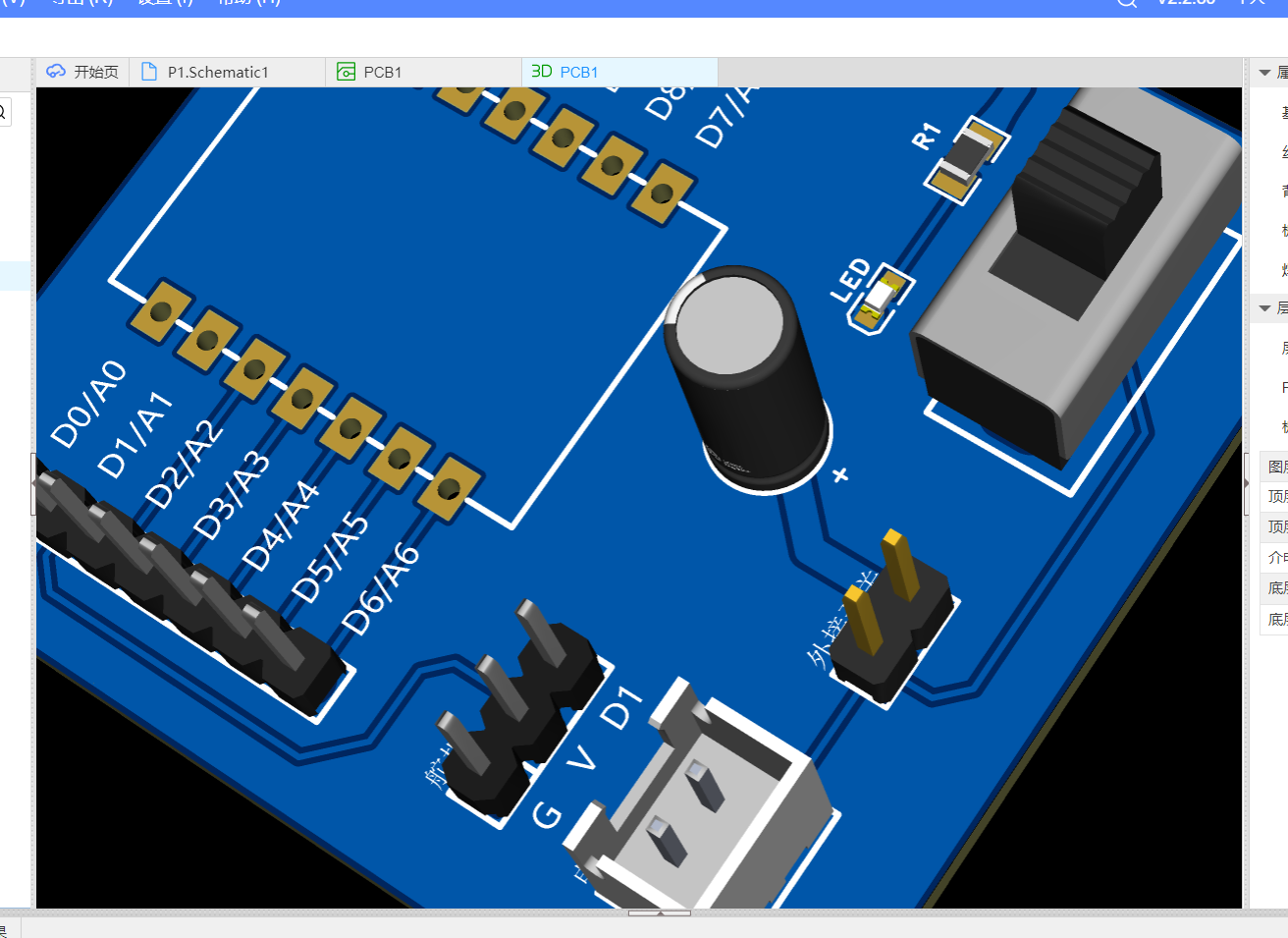
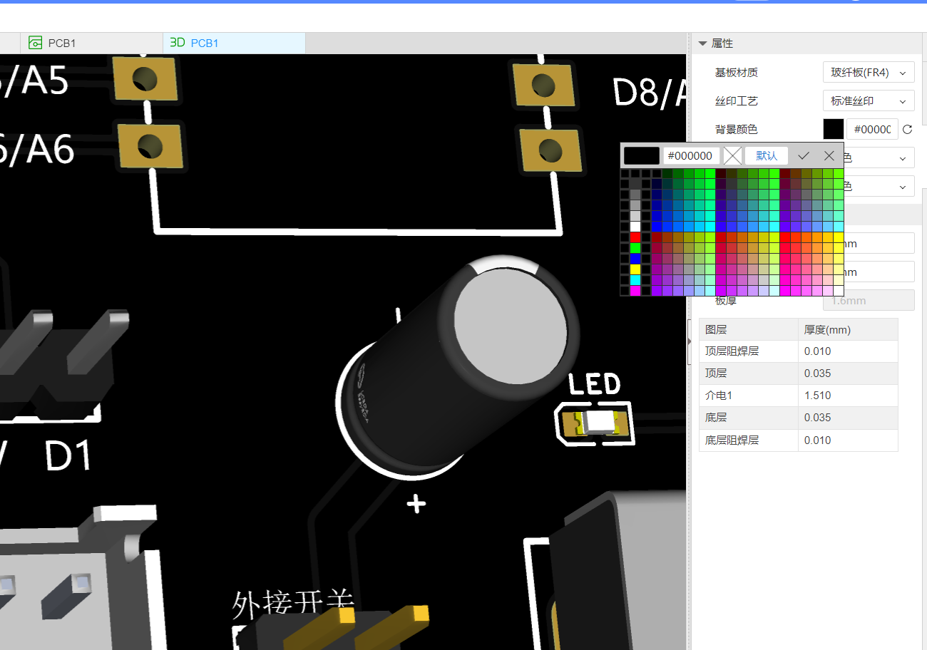
After completing the layout and routing, I generated a 3D preview of the board to visually inspect the component placement and overall design.
To do this, I clicked on "View" in the top menu bar and selected "3D Preview".
This feature allowed me to see a realistic model of the PCB and helped me confirm that all the components were properly aligned and that the board layout was as expected.
For the final look of the board, I customized the appearance settings before placing the fabrication order.
I set the PCB solder mask color to black, giving the board a sleek and professional look.
For the pad finish, I chose ENIG (Electroless Nickel Immersion Gold), which gives the pads a shiny gold color and improves solderability and corrosion resistance.
Final Result
Project Summary
This was my first time independently completing the entire process — from schematic design to PCB layout, fabrication, and soldering — to build a fully functional extension board.
For me, this experience wasn’t just about finishing an assignment; it felt more like a hands-on journey into maker thinking and practical problem solving.
From manually creating the XIAO ESP32-S3 component symbol and footprint, to feeling overwhelmed by a screen full of tangled air wires, and then gradually making sense of everything — I went through a process of exploration, research, trial and error, and iterative improvement.
Throughout this project, I learned:
- How to read hardware pinouts and datasheets to understand circuit structure
- How to use schematic design to express module functionality and build a working system
- How to manually route traces and optimize power and signal paths for better performance and aesthetics
- How to use JLCEDA for custom components, ERC (Electrical Rule Check), and DRC (Design Rule Check)
In the end, my expansion board successfully implemented external button input, servo control interface, and multiple GPIO breakout pins — all functional and ready for real-world use.
ProPrj_Expansion_Board_Base_for_XIAO_1_.epro