Assignment
- use an EDA tool to design an embedded microcontroller system using parts from the inventory, and check its design rules for fabrication
- extra credit: simulate a circuit
- extra credit: try another design workflow
- extra credit: design a case
To design a board I will be using KiCad with the KiCad FabLib which is a library for electronics components schematics and footprints found in the fab inventory. This allows me to design my PCB without separately designing each symbol and footprint.
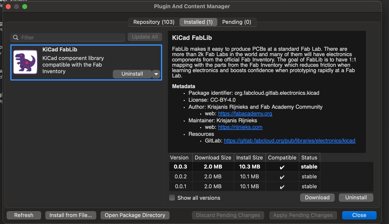
I used the plugin and content manager to download the library by following the README instructions on the GitLab repository. For this board I aimed for a XIAO-based board where I can have input and output pins alongside an I2C connection for future testing.
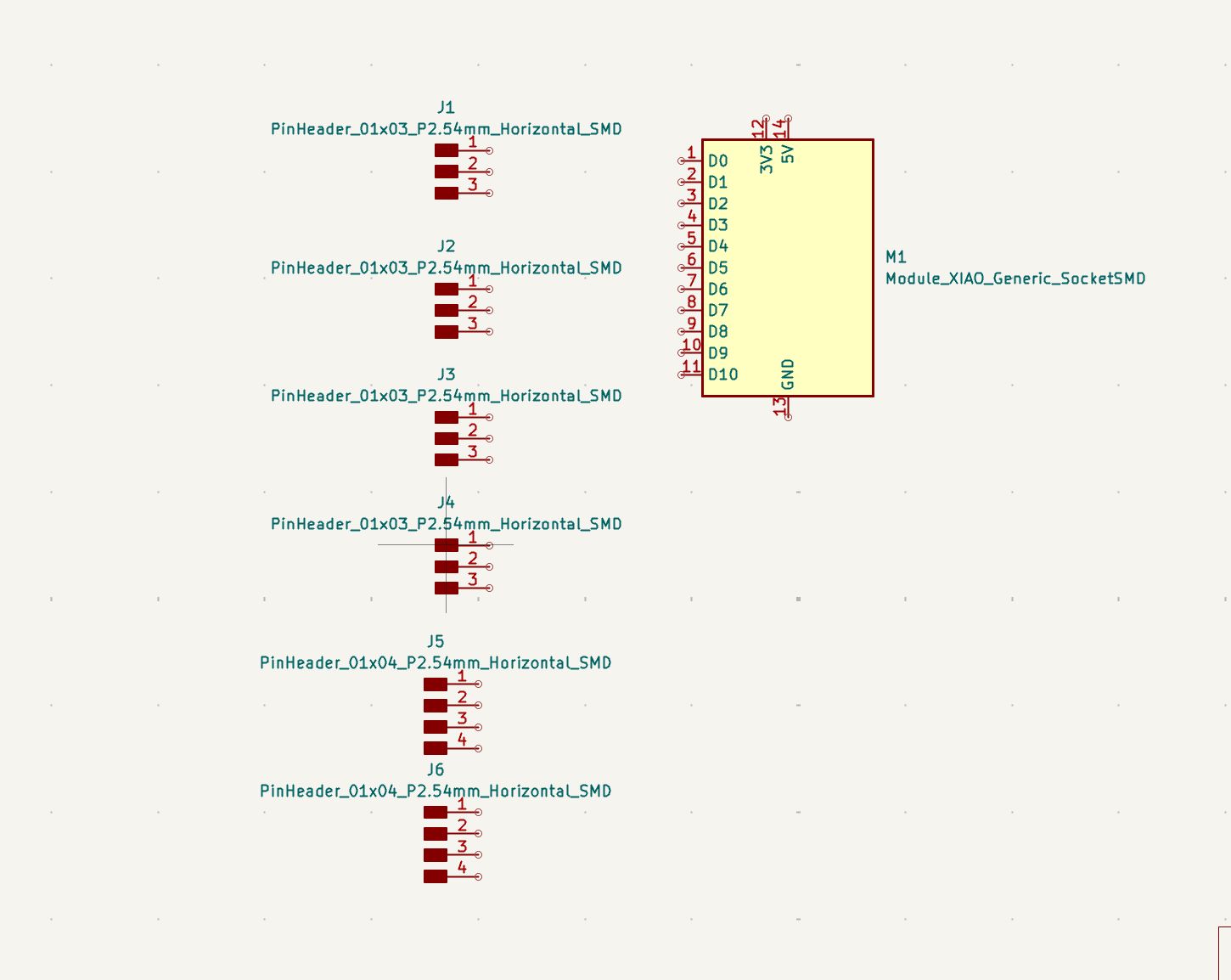
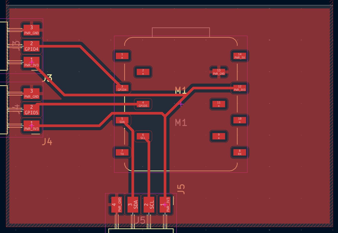
I used 4x 1x3 and 2x 1x4 pin headers and the generic XIAO Socket SMD. Two 1x3 headers are for 3V3/GPIO/GND and the other two are for 5V/GPIO/GND for peripherals. One 1x4 is for I2C and the other is for UART. I preferred the socket so I can swap the XIAO board if needed.
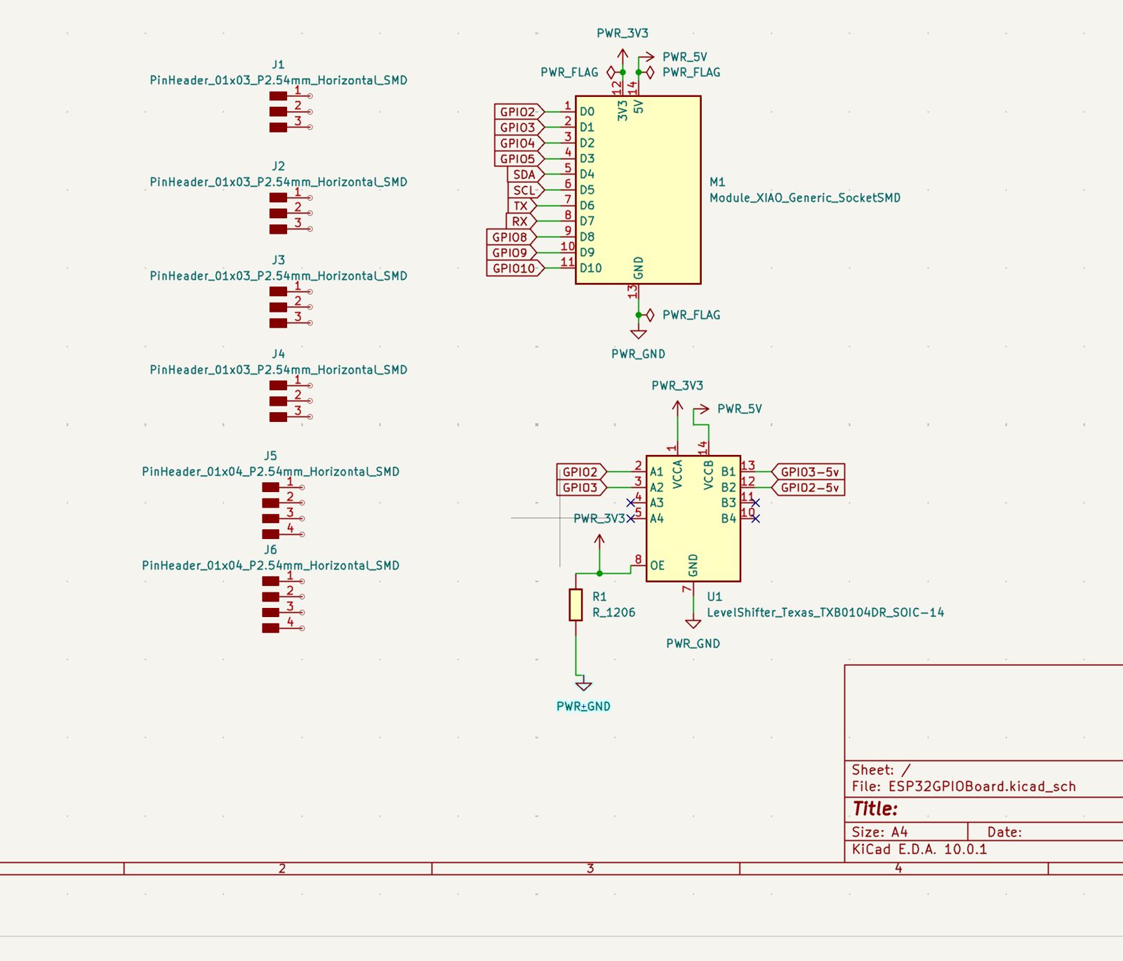
Then I added the level shifter for shifting 3V3 GPIOs to 5V so I can drive 5V logic peripherals like servos. I used global labels for RX, TX, SCL, SDA, and GPIOs, then added power components for 5V, 3V3, and GND. I also added power flags because the board power comes from the USB-C on the XIAO board.
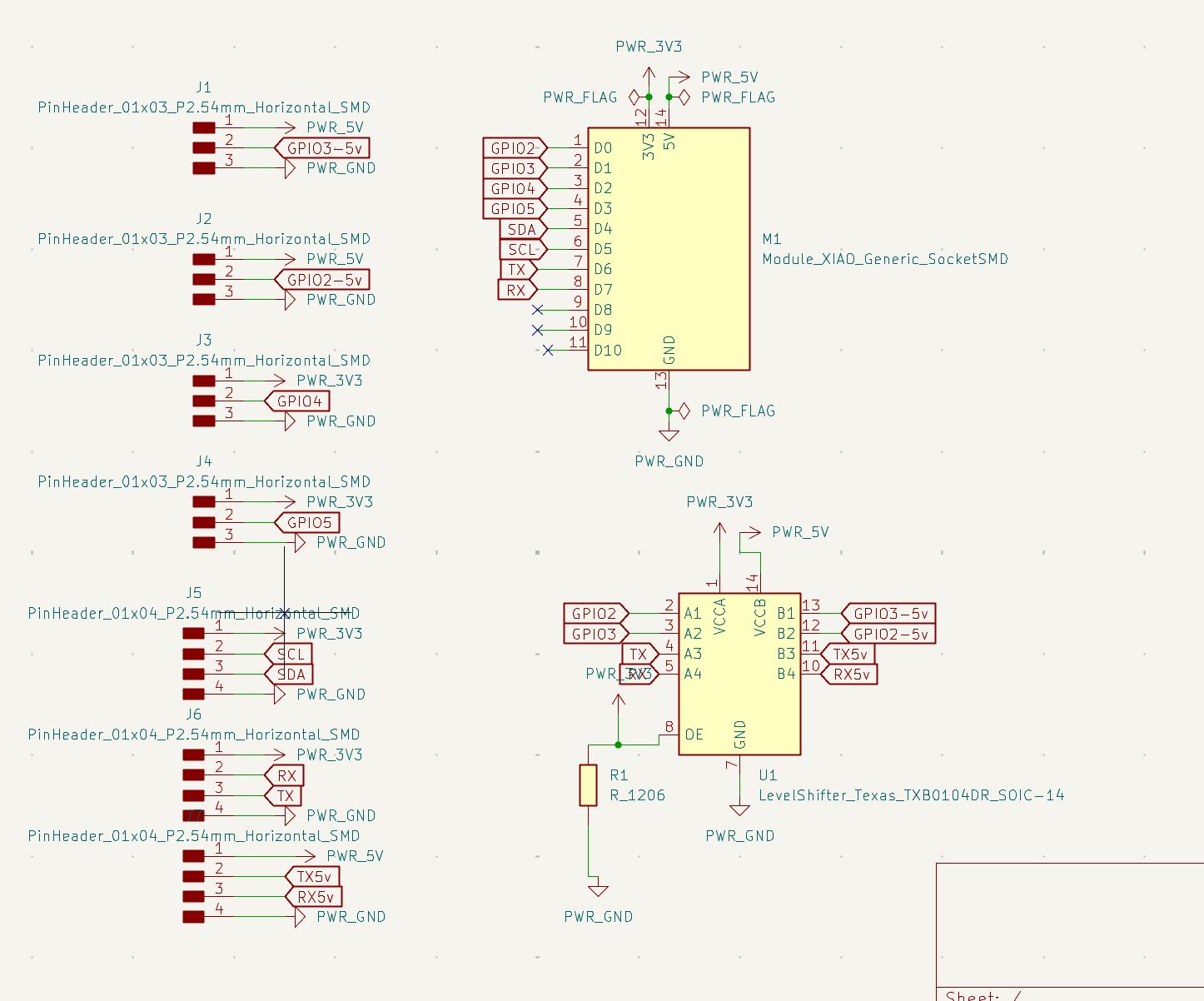
Then I connected all these pins to horizontal pin headers so I can connect the board to peripherals.
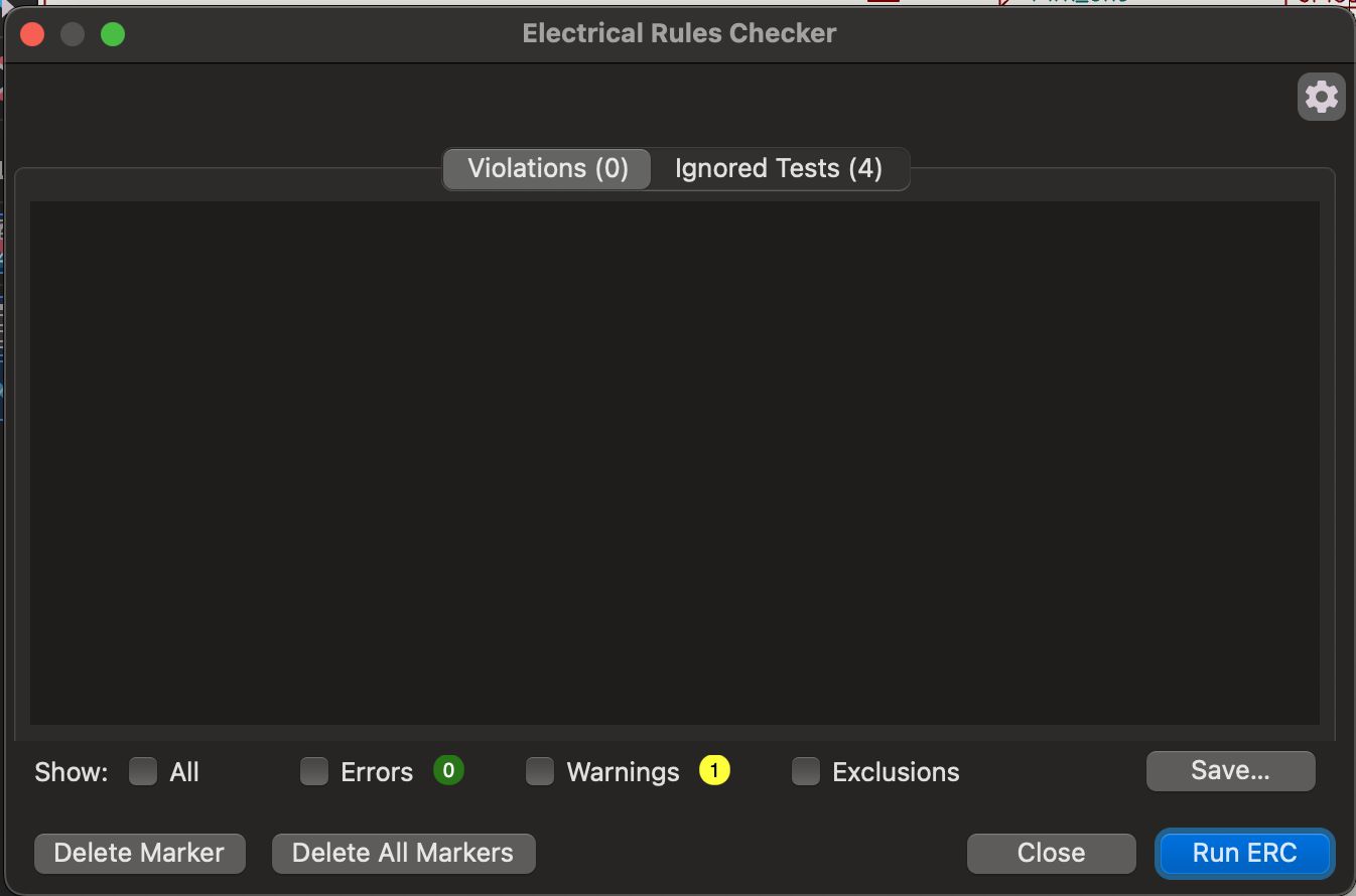
The electrical rules checker came out clean, so I proceeded to PCB Editor.
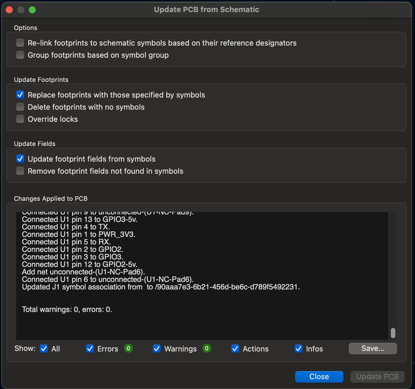
I used “Update PCB from Schematic” to import all footprints.
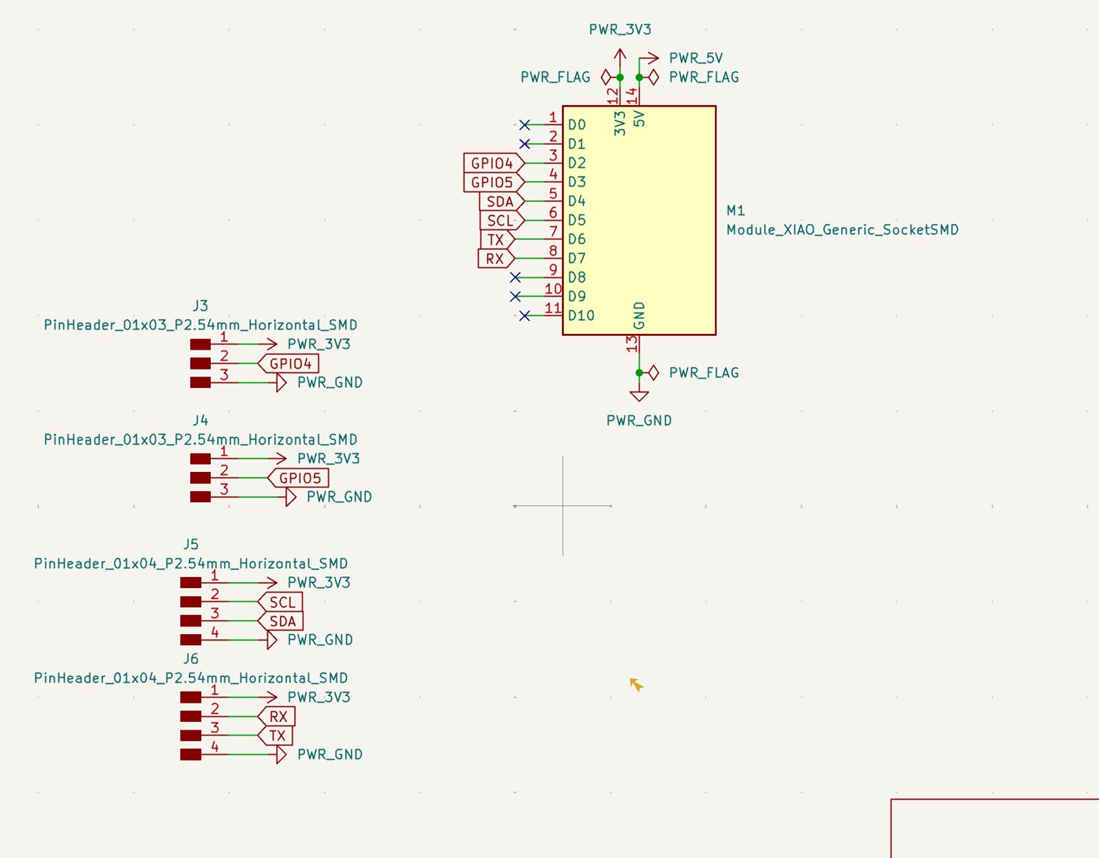
I deleted the level shifter and updated the PCB so it no longer included 5V logic routing.
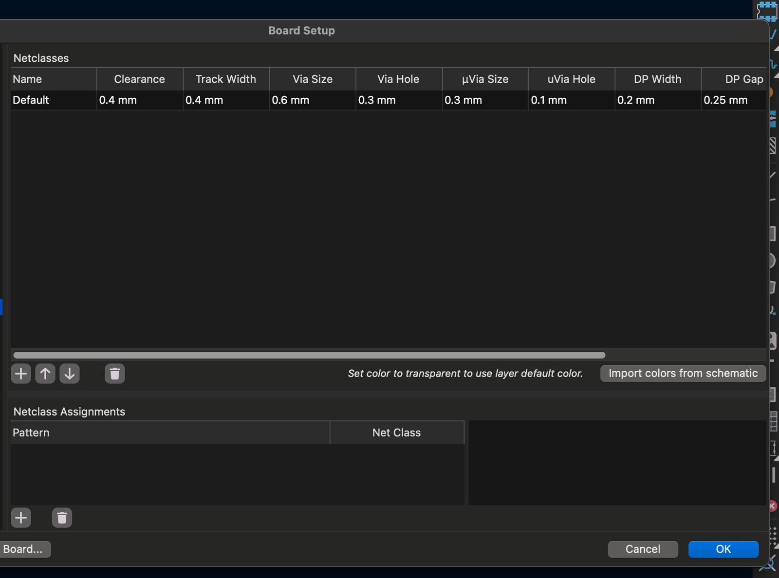
I edited net classes to have 0.4 mm clearance and track width for local milling constraints.
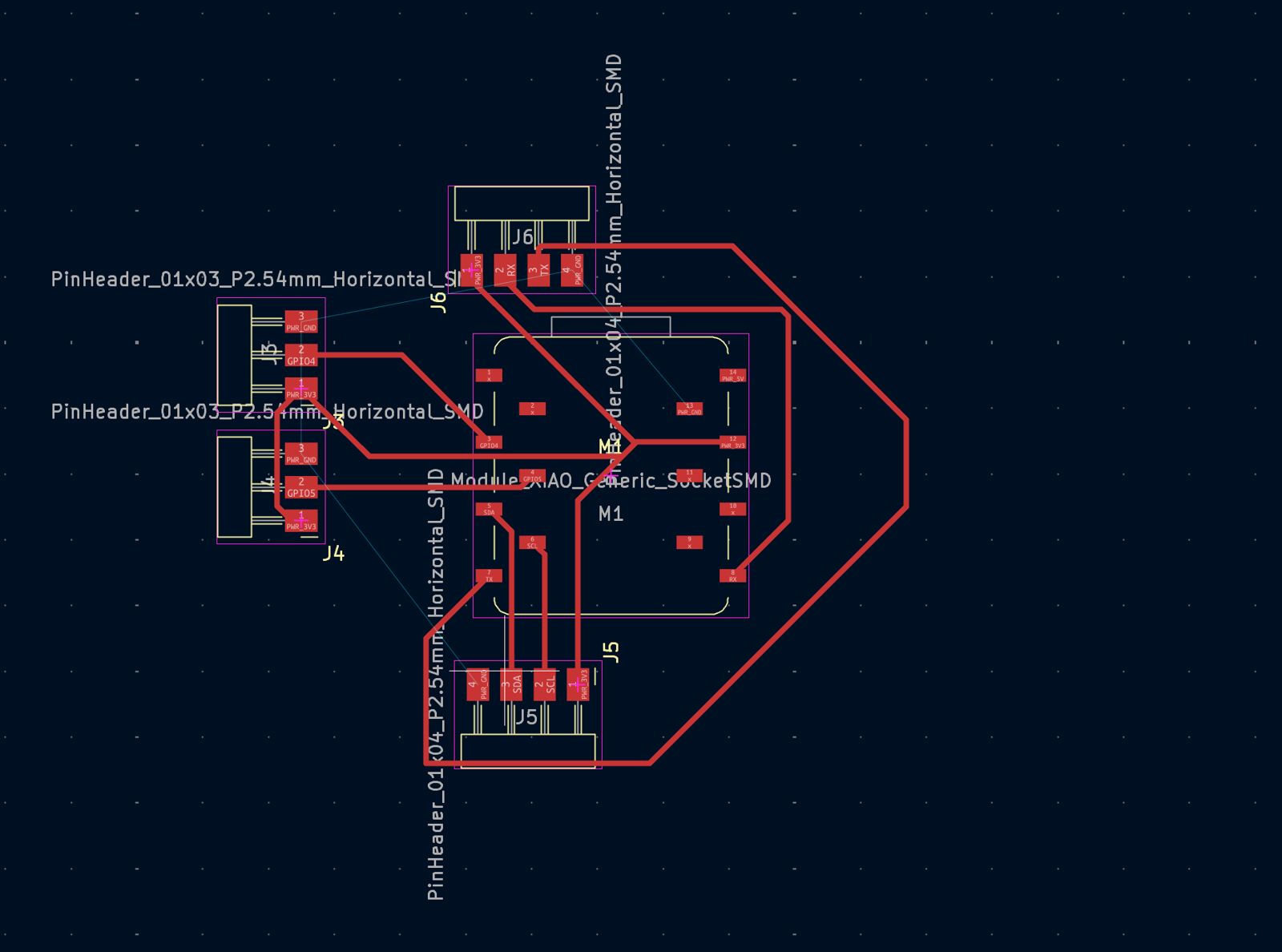
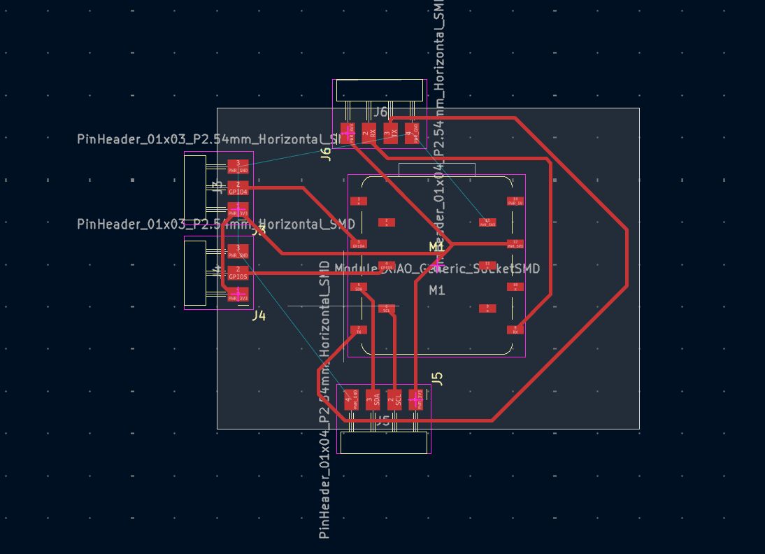
After that I moved components and routed connections according to the schematic. Then I selected Edge.Cuts and defined the PCB outline.
Then I used a filled zone on F.Cu to connect ground.
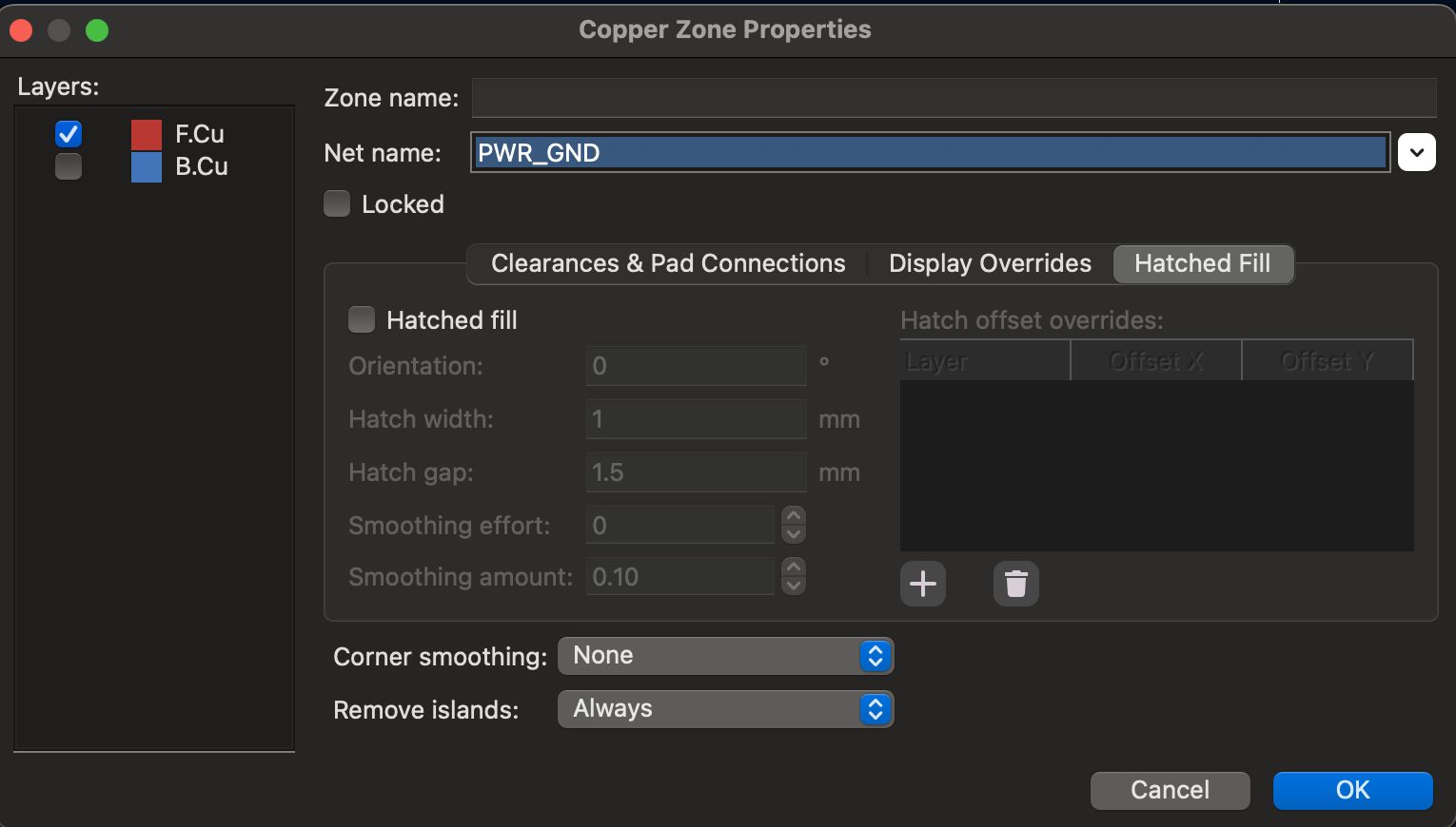
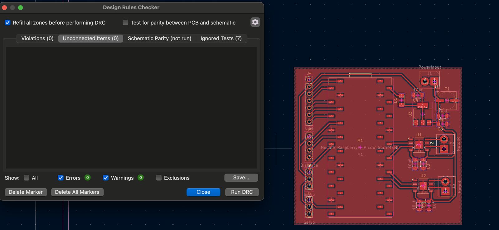
Then I defined the filled zone around the edge cuts and ran DRC.
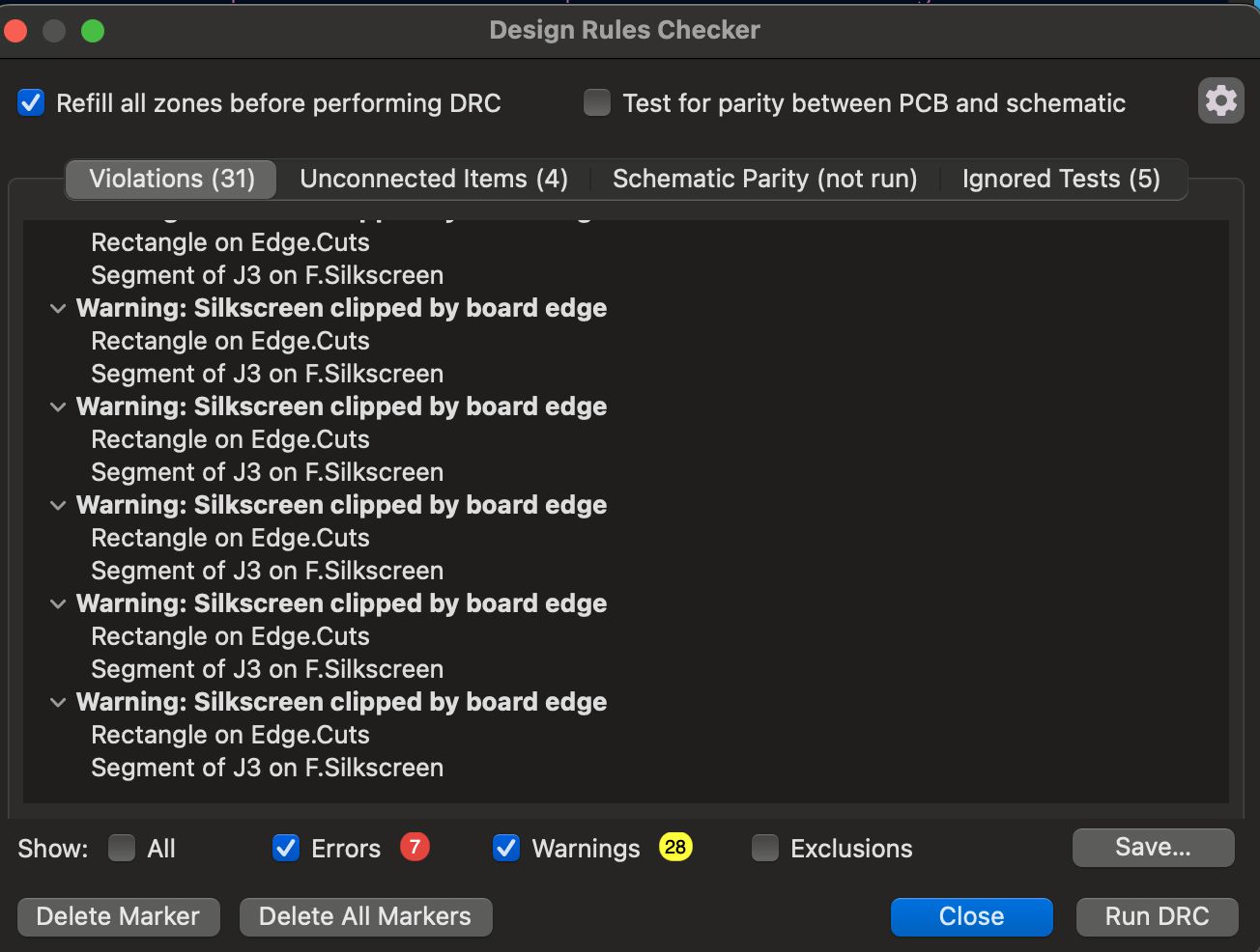
It returned silkscreen clipped warnings, which I ignored because I am not producing silkscreen on this PCB.
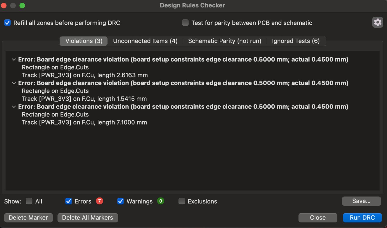
After that I resolved board-edge clearance violations by expanding edge cuts and rerouting where needed. I also removed the UART 4-pin header to simplify rerouting.
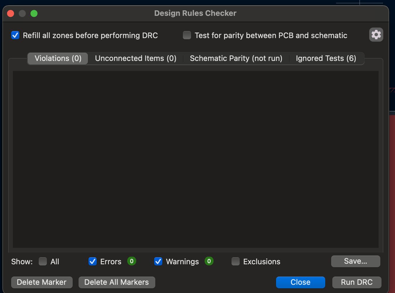
This is the final result and the DRC came out clean.
In conclusion, I designed a board that can connect a XIAO board to GPIO pins and an I2C connection for future use.
Final Project PCB
I want to design a PCB for my final project that features a DC motor driver and GPIO ports for sensor connections and future expandability. I want to use at least an ultrasonic sensor and a line-following sensor, while being able to drive at least 2 DC motors.
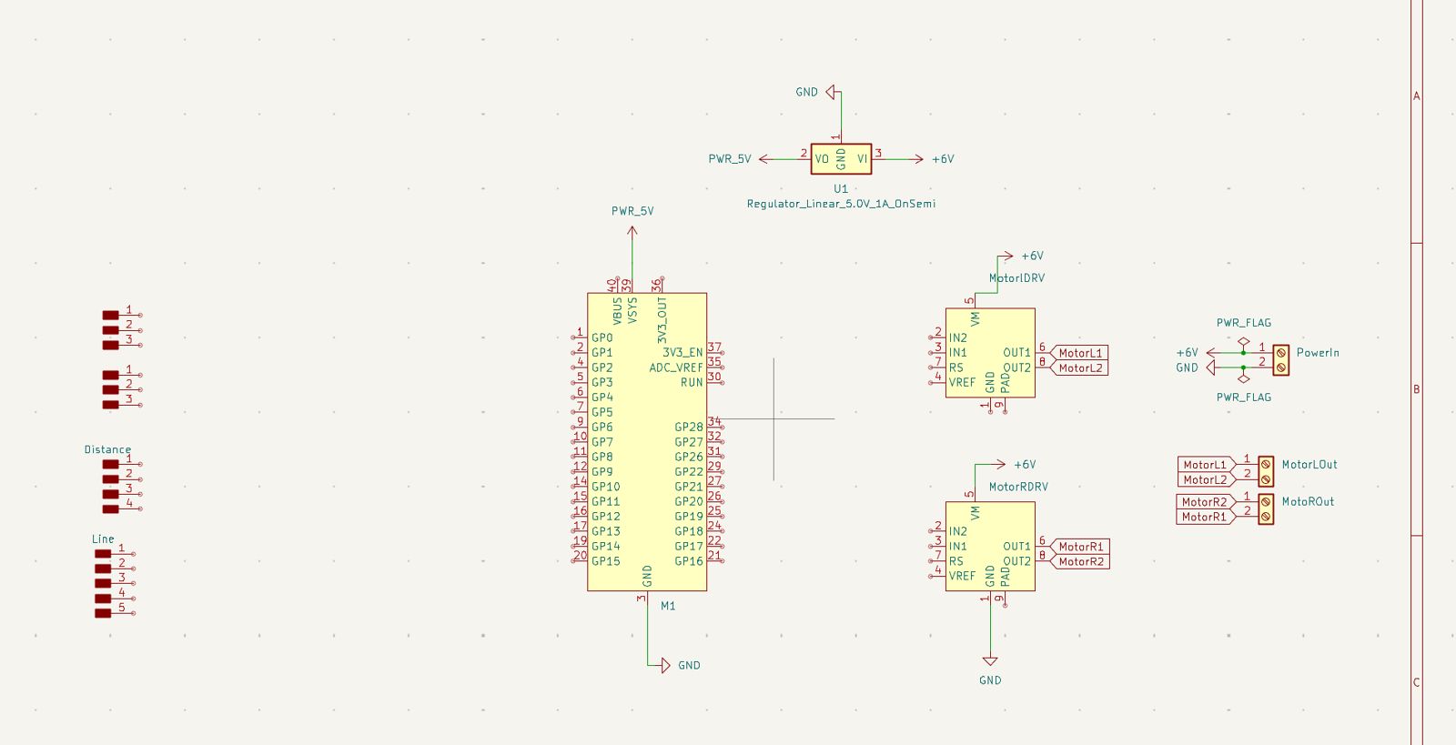
For this version I planned to use a Pico as MCU and power the PCB using 4 AA batteries so it matches DC motor voltage (6V). Since Pico VSYS accepts up to 5.5V, I planned an inline voltage regulator for VSYS. I used the TB67H451AFNG,EL motor controller from Fab inventory for each motor. I added 3 screw terminals (1 power input, 2 motor outputs), 2 vertical 1x3 headers for servos, 1 1x4 for distance sensor, and 1 1x5 for a 3-array line-following sensor.
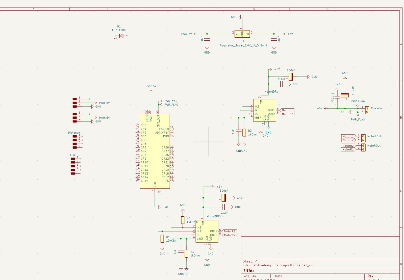
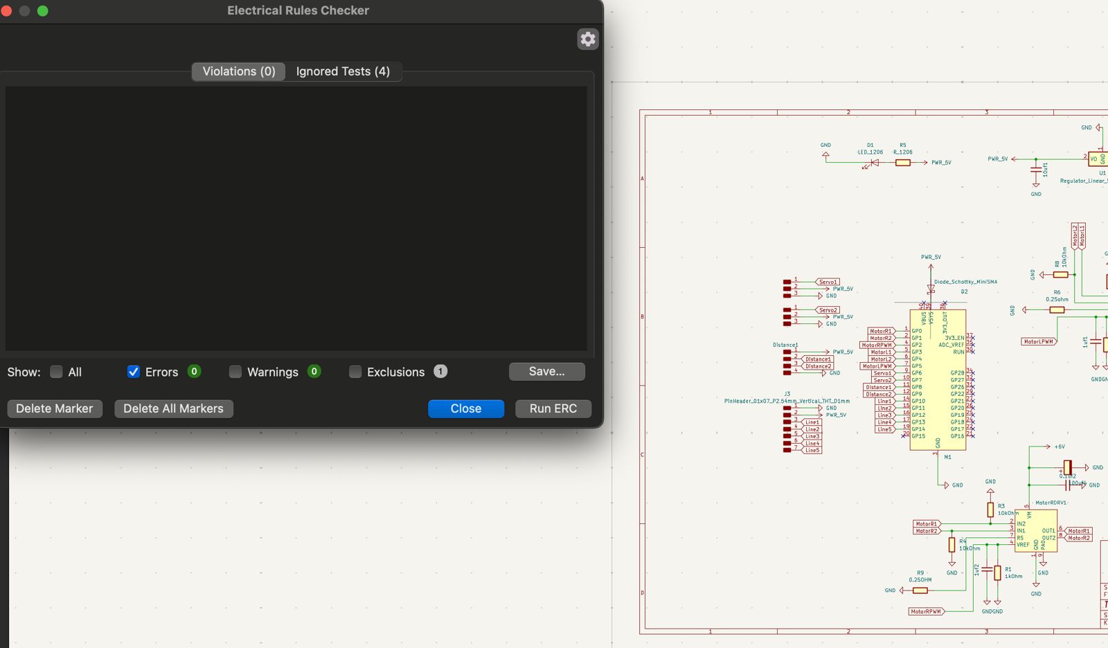
Then I added capacitors and resistors where needed. Capacitors are placed where stable current is needed, such as motor controller power inputs, before and after the voltage regulator, and main power input. I also added resistors on motor inputs and PWM lines to filter noise, then ran ERC.
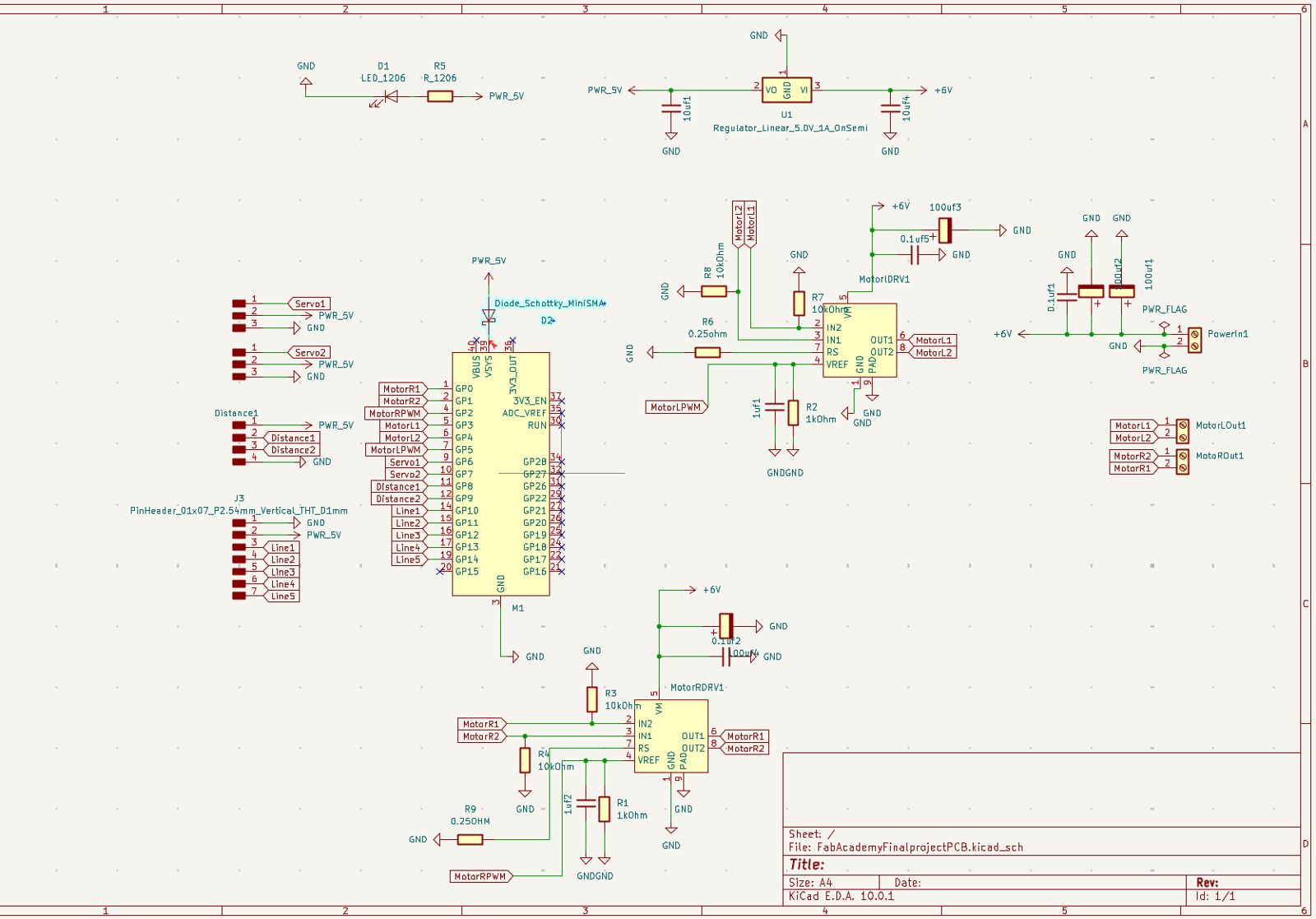
This is how the final schematic looks.
Then I proceeded to PCB Designer to route the board.
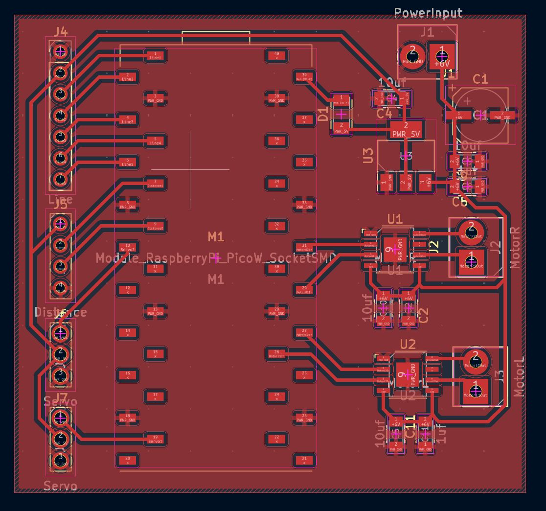
I connected each connector, made a ground fill zone, and ran DRC which came out clean.