KiCad
I downloaded KiCad and this GitHub repository by Krisjanis Rijnieks. These components are avaliable in all the labs so its convenient to use them for the production process.
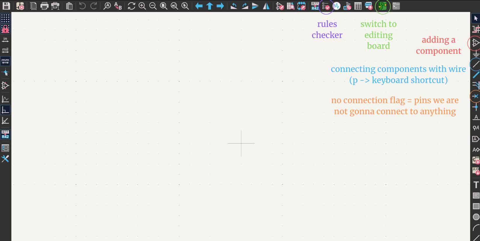
Explanation of the basic KiCad tools I used for my design:

After I cut out my first design I realized that the track widths were way too thin and it was about my KiCad Settings.
Track: use netclass width > Net Classes > Changed my settings to this:

Board 1
I wanted to start out by an easier desing first to get used to working with KiCad. I made a simple board with esp32c3, a led and a resistor.

Board 2
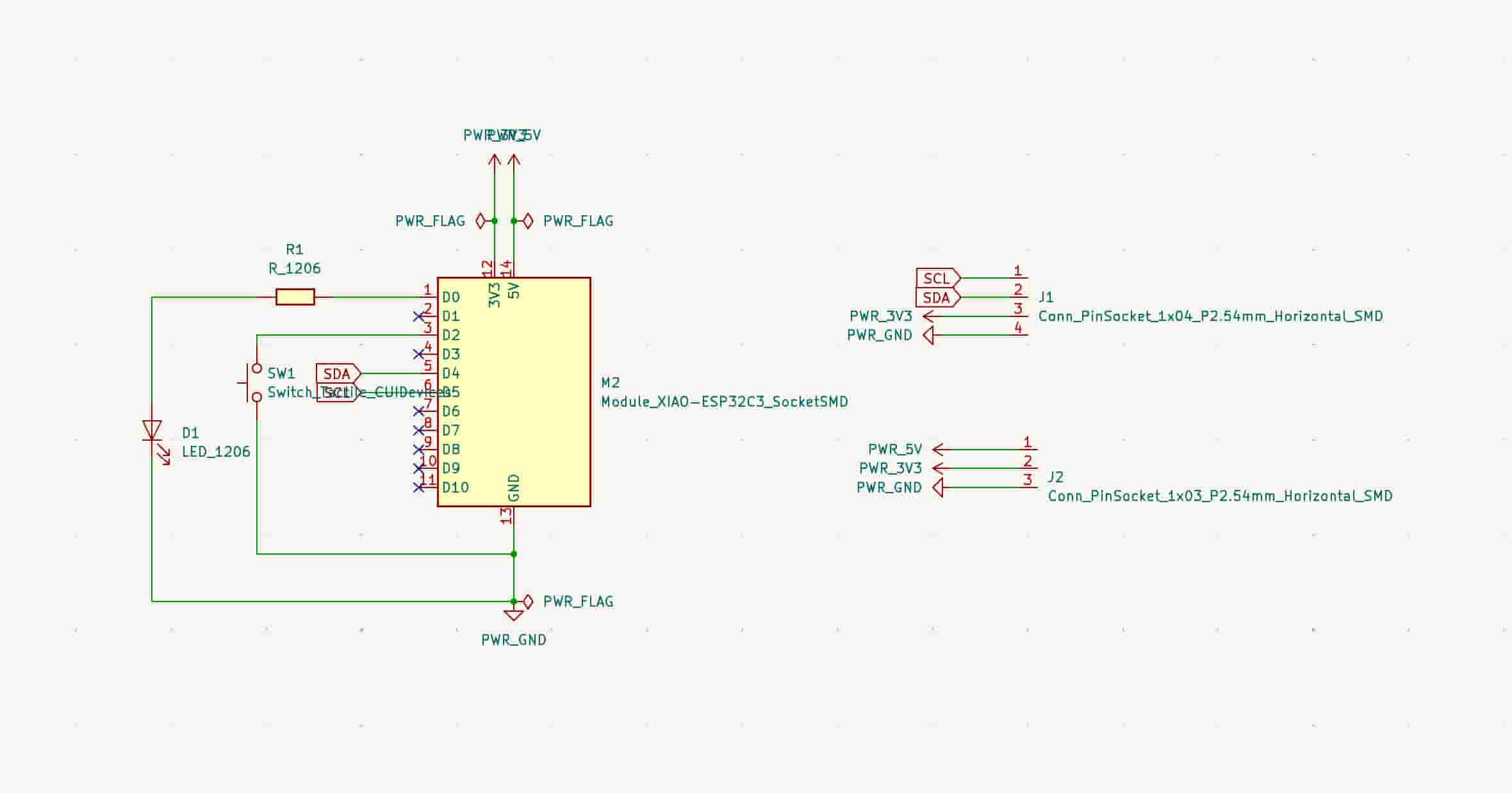
Here is the schematic design i made:

Here are the components:
- Main microcontroller: seeed studio xiao esp32c3
- LED 1206 with the Cathode (+) connected to GPIO2 and Anode (-) connected to GND
- Resistor 1206 between LED and GPIO
- Switch
- 4-Pin header for I²C Communication
PCB Editor - Design 1
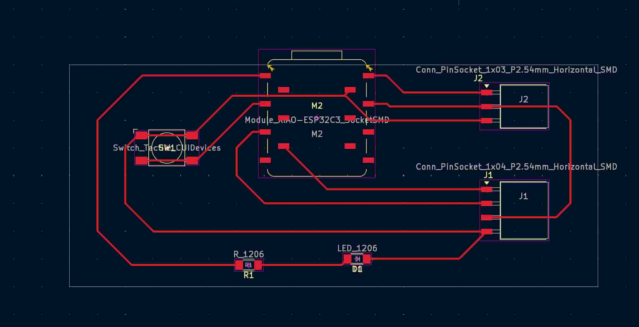
For my first design of this board I did a direct GND Connection to ESP32-C3
I opened the design in pcb editor and organized the parts. I clicked Route Tracks and the components I had to connect were highlighted.

PCB Editor - Design 2
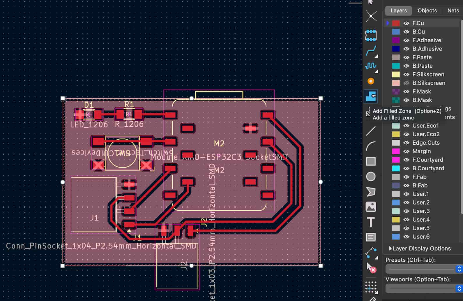
For my second design of this board I used a Ground Plane as GND
Here is a comparison of the two different methods:
| Direct GND Traces | Ground Plane |
|---|---|
| Poor Voltage Stability | Good Voltage Stability |
| Poor Thermal Dissipation | Better Thermal Dissipation |
| Poor Routing Simplicity | Easier Routing |
So it is better practice to use ground plane as gnd. To do this I selected F.Cu from Layers and added a Filled Zone:
Selected Filled Zone:

Select GND:

And then drew a rectangle around the components and pressed B on the keyboard. I pressed on the rectangle outline and Shape Modification > Fillet to make the edges round:

Adding a Filled Zone causes the gnd parts to look like this after printing the board. The cut outs in the squares allows flow between all the gnd parts after soldering.

Group Assignment
Here is our group assigment
File
Here is the zip files for the pcb design