This week I will start studying electronic design, which will be another great challenge for me, learning to draw a circuit board through video tutorials, designing an embedded microcontroller to use sound to control lights, which is really interesting.
Learning Objectives
Group assignment:
Use the test equipment in your lab to observe the operation of a microcontroller circuit board (as a minimum, you should demonstrate the use of a multimeter and oscilloscope)
Individual assignment:
Select and use software for circuit board design
Demonstrate workflows used in circuit board design
I used AI assistance to help me learn while summarizing the webpage content about the VICTOR 270 oscilloscope and the VICTOR VC890C multimeter for this week’s assignment.
Group Assignment
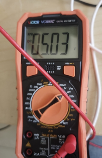
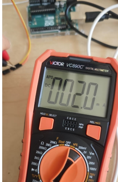
The main task has been completed: using the VICTOR 270 oscilloscope to test the waveform of an LED controlled by a button, and using the VICTOR VC 890C multimeter to measure the corresponding current and voltage values.
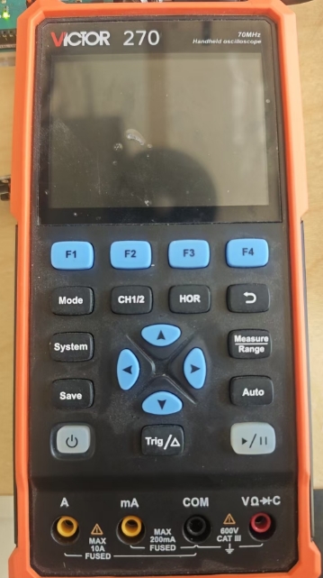
1.1 VICTOR 270 Oscilloscope
Introduction
The VICTOR 270 is a compact, handheld digital oscilloscope with a bandwidth of 70 MHz.
Power on the device by pressing and holding the power button.
Connect the probe: GND clip to ground, probe tip to the signal point (e.g., an Arduino pin).
Set the probe to 1X mode and ensure the oscilloscope input matches.
Adjust V/Div (voltage per division) to scale the signal properly, e.g., 2V or 5V/div.
Adjust Time/Div based on signal speed — start with 10ms/div for button press waveforms.
Use Trigger settings (edge trigger, CH1, ~2.5V) to stabilize the waveform.
Observe the waveform and use measurement tools if needed (frequency, voltage, duty cycle).
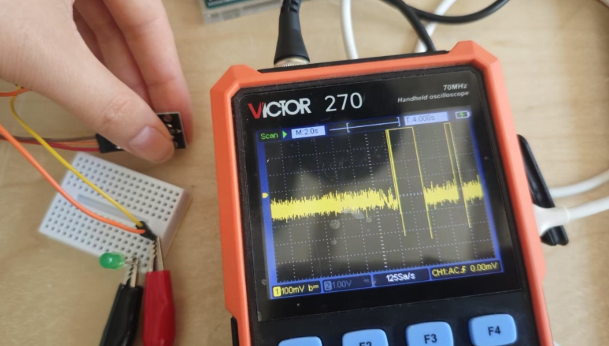
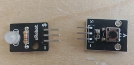
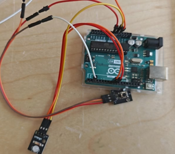
1.2 Using VICTOR 270 Oscilloscope to Test an LED Controlled by Button
1.2.1 Objective
Use the VICTOR 270 handheld oscilloscope to observe the waveform of an LED controlled by a button on Arduino UNO.
1.2.2 Circuit Overview
Component
Arduino Pin
Description
Button
D2
Using internal pull-up; press to LOW
LED
D13
With resistor to GND
1.2.3 Test Points
Test Point
Why
Expected Waveform
D10 (LED output)
Best choice: shows output waveform
HIGH (LED ON) ↔ LOW (OFF) square wave
D2 (button input)
Optional: input signal
LOW when pressed ↔ HIGH when released
1.2.4 Oscilloscope Settings
Probe: CH1 to D10, GND clip to Arduino GND
Voltage (V/Div): 5V/div
Time (Time/Div): 20ms/div to 100ms/div
Trigger: Edge trigger, rising or falling, CH1, level ~2.5V
Probe setting: Set to 10X on both probe and scope
1.2.5 Waveform
When button is pressed, D10 goes HIGH (LED ON); released, goes LOW (LED OFF).
    5V ─────────┐       ┌────────────
                     └───────┘
    0V
Video
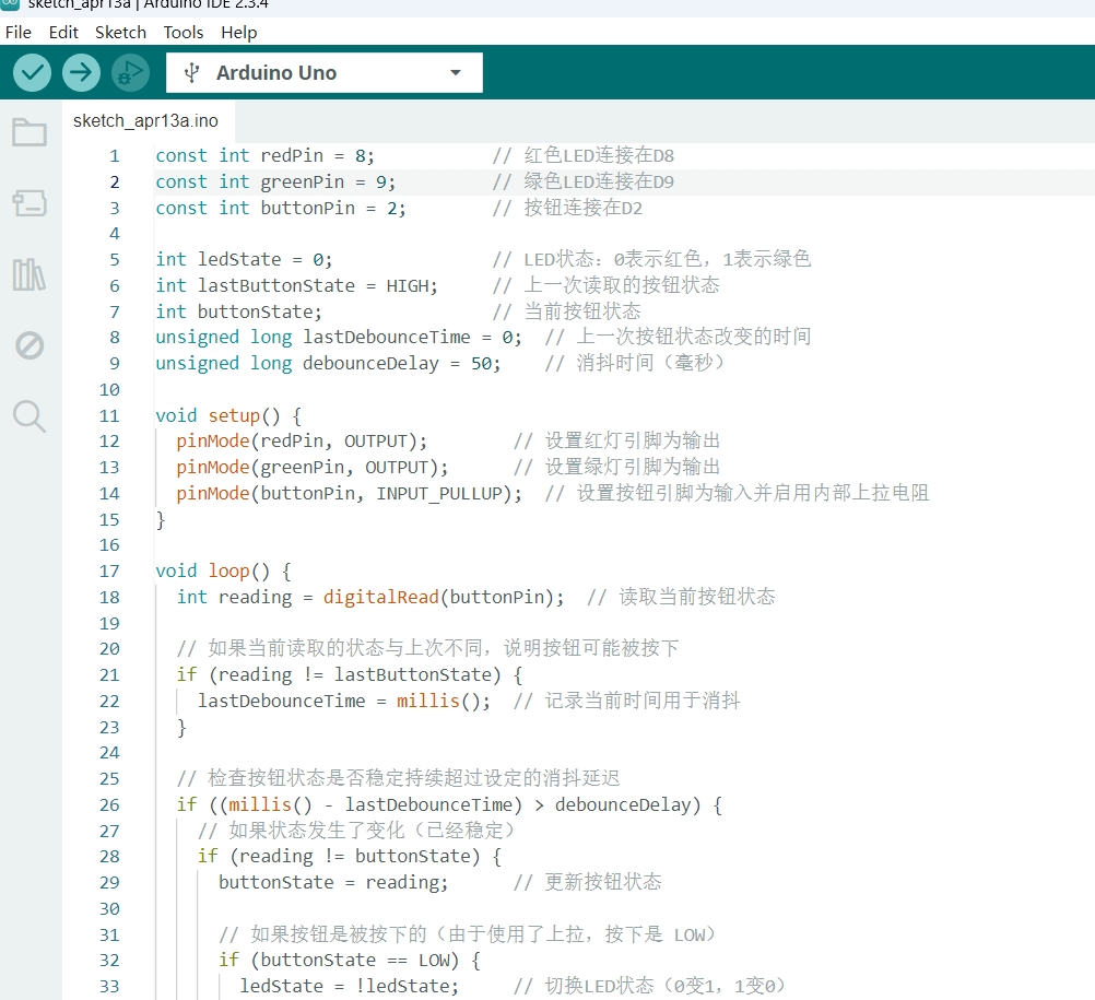
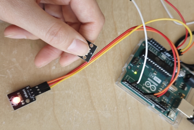
Button-controlled Dual-color LED
Button-controlled Dual-color LED is a simple yet practical project that demonstrates how to use a push button to toggle between two LED colors—red and green.
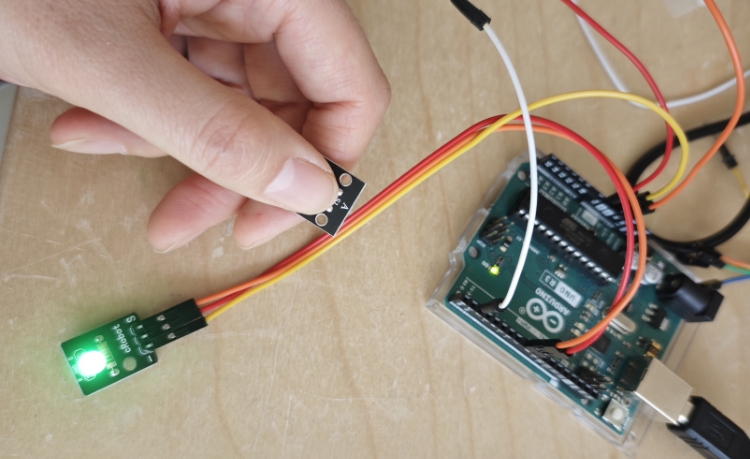
The VICTOR VC 890C is a professional-grade digital multimeter capable of measuring voltage, current, resistance, capacitance, temperature, frequency, and more.
Turn the rotary switch to the desired measurement mode (e.g., V for voltage, A for current).
Connect the black probe to the COM terminal.
Connect the red probe to the corresponding terminal:
VΩHz for voltage, resistance, frequency
mA or 10A for current (depending on expected range)
Ensure the measurement range is set correctly (use auto if unsure).
Apply the probes to the circuit points and read the value on the display.
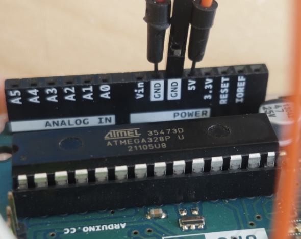
1.4 Example
Measuring the voltage and current of the 5V pin on the Arduino UNO board using a multimeter.
Individual Assignment
1 What is electronic design?
1.1 Introduction
It refers to the process of planning, designing and realizing the circuit and its components in the development of electronic products. It involves hardware design (such as circuit schematic design, PCB design) and software programming (if embedded systems are involved). It is a key link to transform theoretical knowledge into practical and usable electronic devices.
Identify product objectives and functional requirements, and provide lighting to facilitate nighttime operations.
Scheme Formulation
Select the right materials and determine the design cost.
Schematic Design
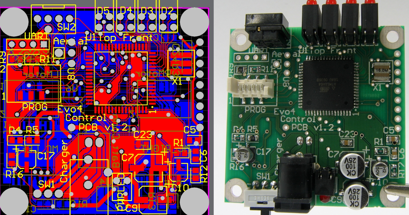
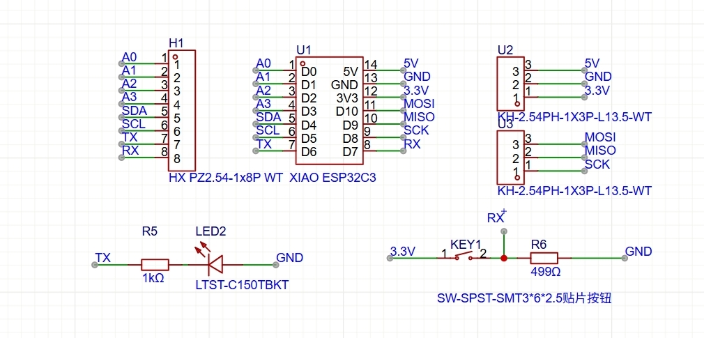
Use EDA software (such as KiCad, Eagle) to draw circuit schematics, defining the electrical connections between components.
PCB Design
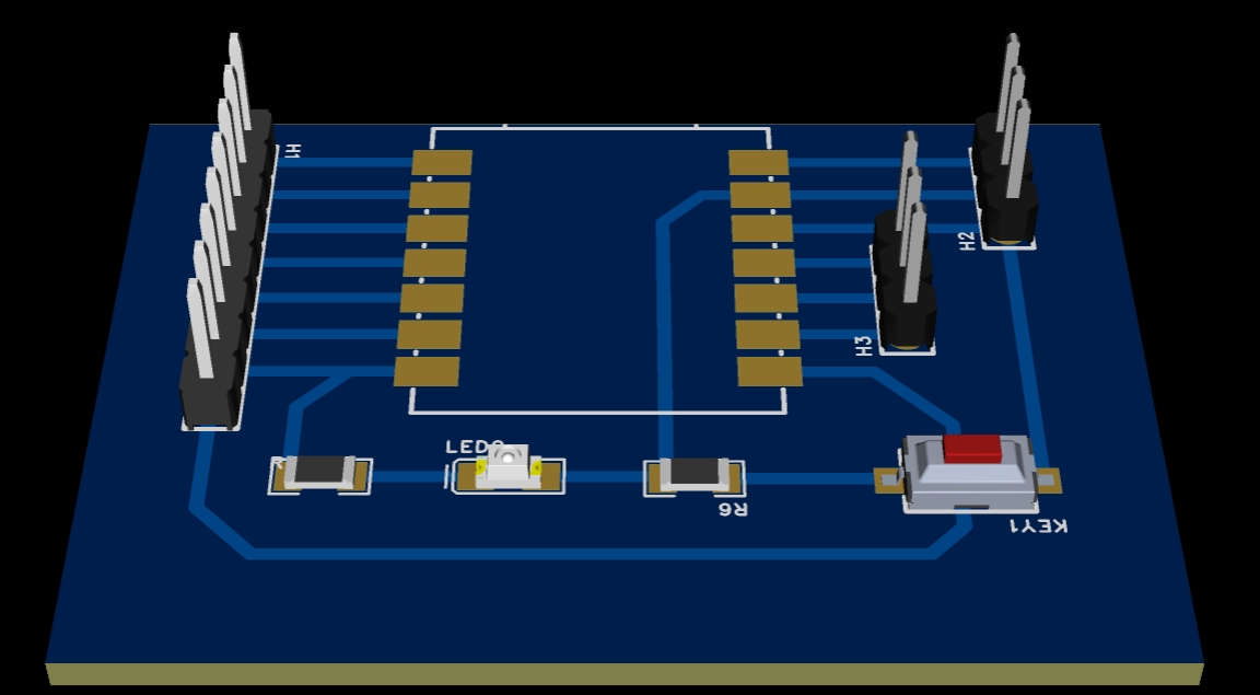
Complete PCB layout and routing in EDA software to ensure that both electrical performance and physical dimensions meet design specifications.
Prototype Fabrication
Utilize PCB manufacturing processes to produce physical circuit boards, proceed with component soldering and assembly to create a testable prototype.
Debugging and Optimization
Conduct functional and performance testing on the prototype, identify and resolve potential issues, optimize designs.
Production Preparation
Assemble the prototype according to the material and design.
2 EDA(Electronic Design Automation)
LC EDA is an online electronic design automation tool developed by a Shenzhen-based company specifically for circuit design and PCB design, providing a complete solution from schematic design to PCB layout. It is cloud-based, with a rich component library, powerful simulation capabilities, and integrated PCB design and manufacturing services to support team collaboration and resource sharing.
2.1 Register an account
EDA official websitelceda website And create an account.
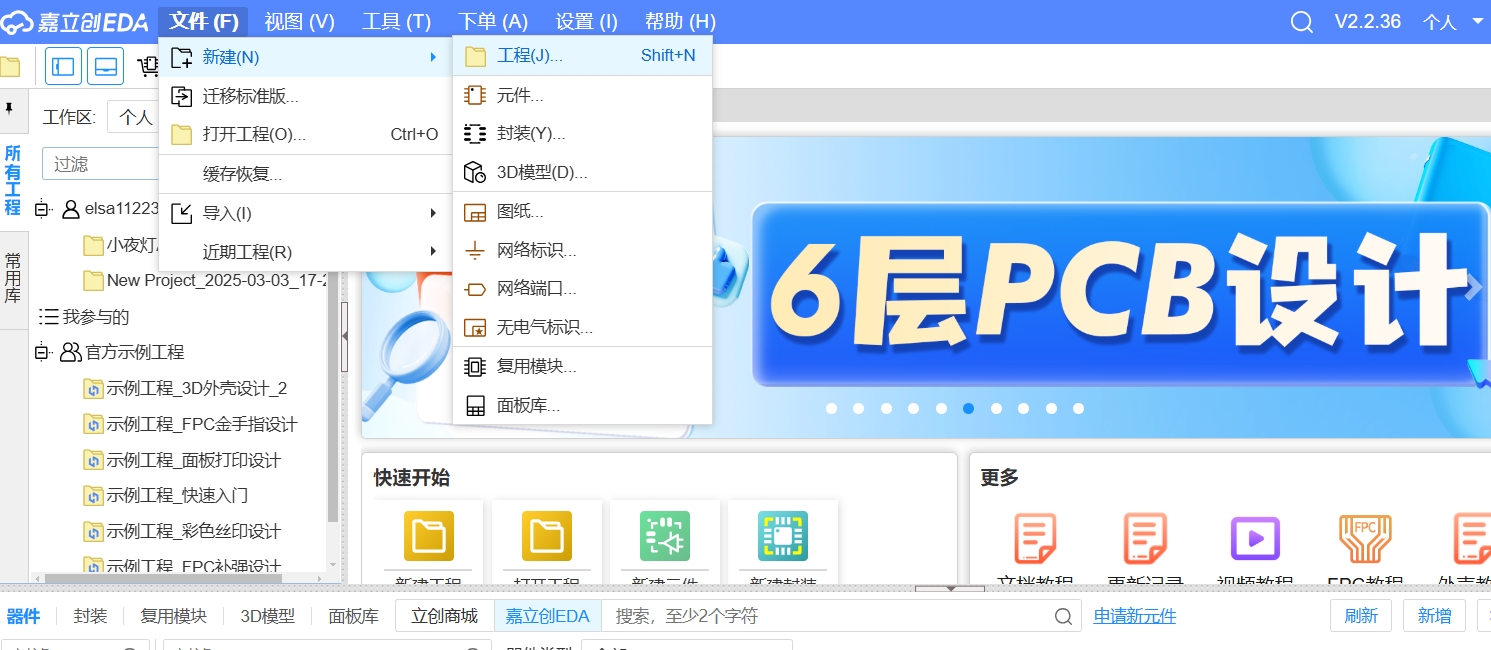
2.2 Create a project
After logging in to the Pro Edition, click the "New Project" button to create a project.
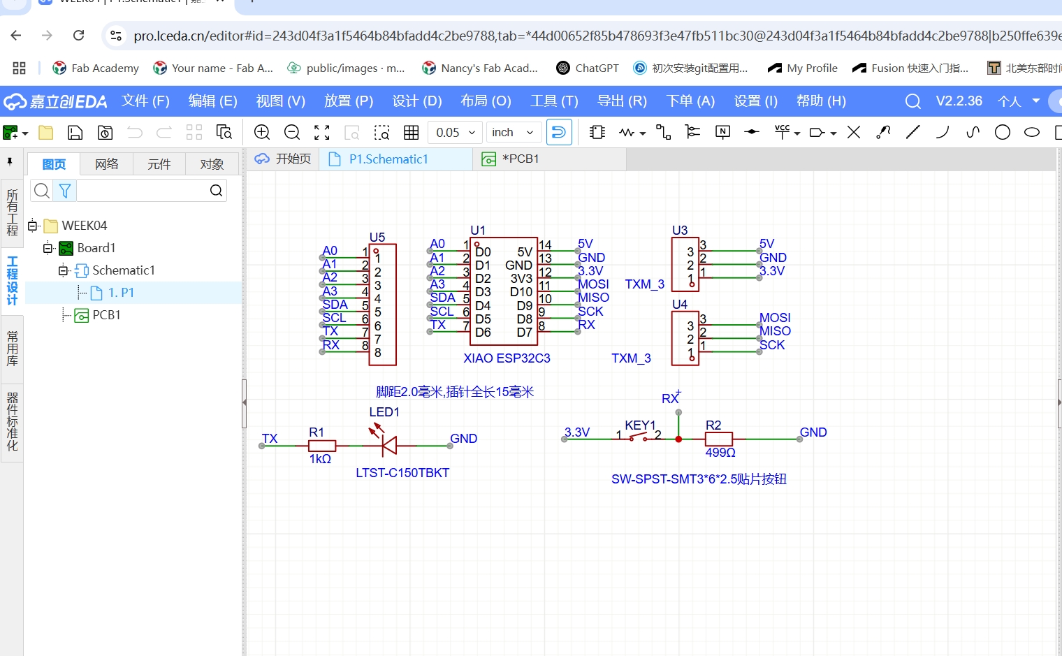
2.3 Draw the design schematic diagram
Refer to the learning video(Video reference),use the built-in component library to draw the circuit schematic, add the necessary components and connect.
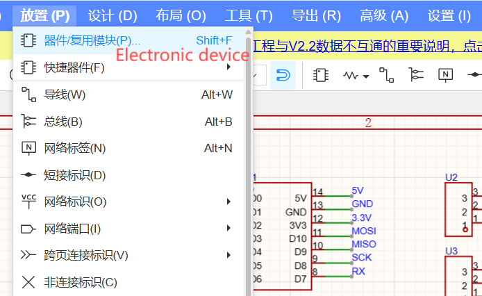
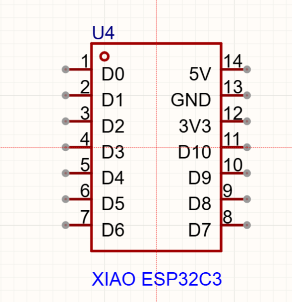
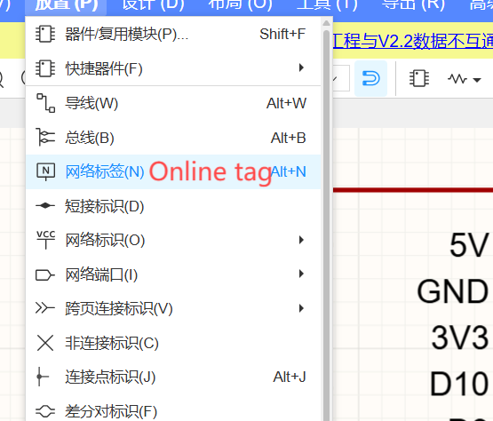
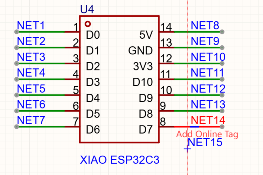
Click Place - Component
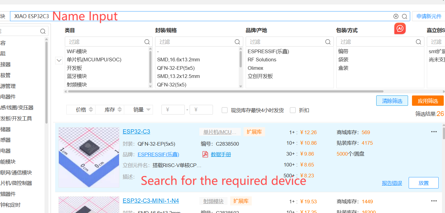
Enter the component name in the search box and select the model you purchased
Click the mouse to place the component on the canvas
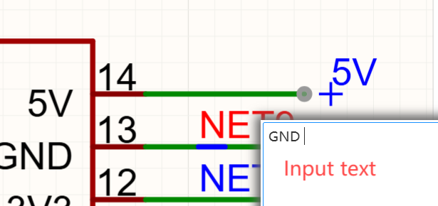
Click Place - Add online tag
Connect one by one
Enter the tag name
Finish the design
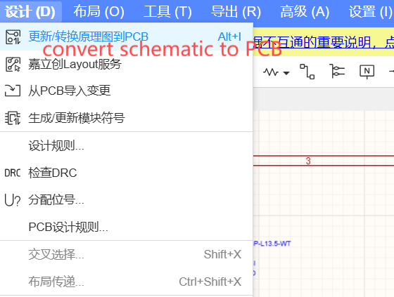
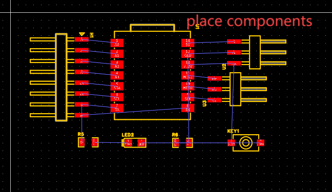
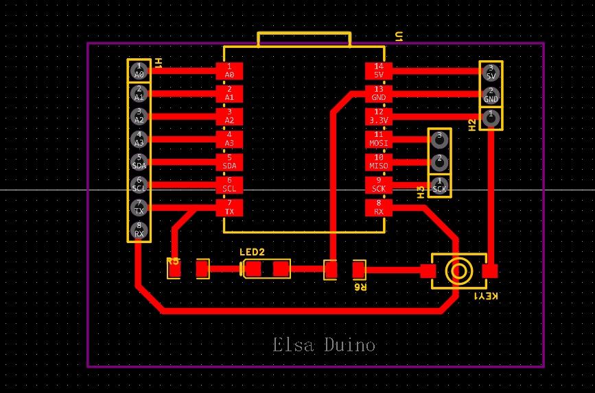
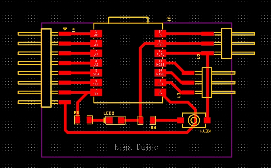
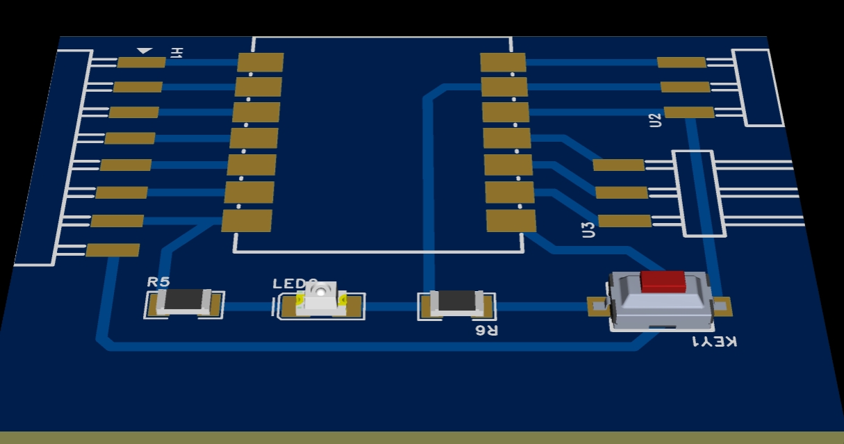
2.4 PCB layout
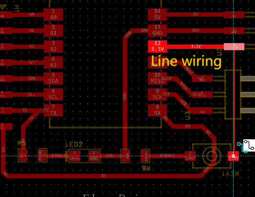
Generate PCB layout according to schematic diagram, adjust component position and route.
Design - Convert schematic to PCB
Arrange the components
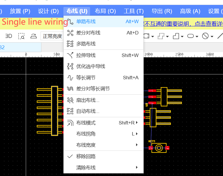
Routing - Single Track Routing
line Wiring
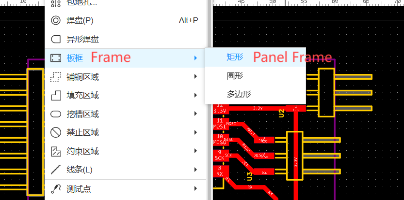
Click Place - Frame - Panel Frame
Board Frame
Place - Text
Input Text
2.5 Design Notes
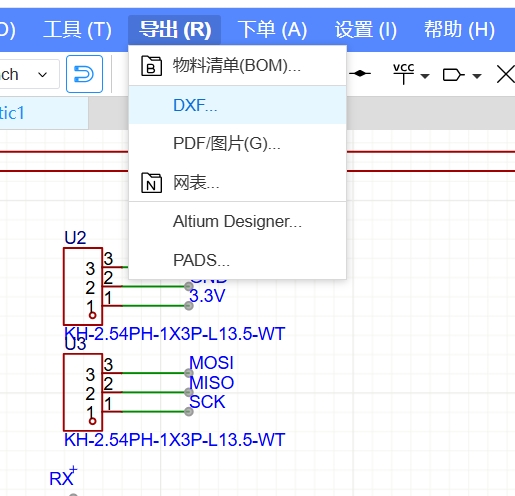
File Export
Export the necessary production files (e.g., Gerber files, BOM, drill files) for PCB manufacturing.
2.5 Version Optimization
2.5.1 Design Considerations
Component Selection: Use 1206 packages for resistors and LEDs, switches.
Pin Header Type: Choose between right-angle (horizontal) or straight (vertical) pin headers, with a standard pitch of 2.54 mm.
2.5.2 Through-Hole Version (V1)
Ensure the hole diameter is larger than the pin header diameter to allow proper insertion.
Avoid setting hole sizes too small to prevent poor soldering or mechanical stress.
2.5.3 Surface-Mount (Horizontal) Version (V2)
Based on PCB size, consider enlarging the pad area to cover more of the pin length.
This allows for better solder contact and improved mechanical strength during assembly.