6-Electronic Design
Assignments
Group assignment:
- Use the test equipment in your lab to observe the operation of a microcontroller circuit board (as a minimum, you should demonstrate the use of a multimeter and oscilloscope)
- Document your work on the group work page and reflect what you learned on your individual page
Individual assignment:
- Use an EDA tool to design a development board that uses parts from the inventory to interact and communicate with an embedded microcontroller
Include in documentation
- Linked to the group assignment page
- Documented what you have learned in electronics design
- Checked your board can be fabricated
- Explained problems and how you fixed them.
- Included original design files (Eagle, KiCad, etc.)
- Included a ‘hero shot’
The road map i made for this week can be accesed here
Group Assignment
We were firstly tasked to use the test equipment in the lab to observe the operation of a microcontroller circuit board (as a minimum, you should demonstrate the use of a multimeter and oscilloscope)
⚡ DC Voltage (Direct Current)
Flows in one direction only.The voltage stays constant, and it comes from batteries, solar panels, USB charger.Can be used in electronics
Example: A AA battery gives 1.5V DC
⚡ AC Voltage (Alternating Current)
Changes direction back and forth.The voltage goes up and down like a wave.It comes from wall outlets (mains power)and its used in fridges, washing machines, lights
Example: Wall sockets give 230V or 120V AC, depending on where you live.
Additional Understanding
🔌 Resistance (Ω) How much a material resists the flow of electrical current. Unit is in Ohms (Ω)
⚡ Continuity Whether or not there is a complete path (connection) for electricity to flow.The multimeter beeps if the path is complete — no beep means a break in the circuit.
🔋 Capacitance (F) A component’s ability to store electrical charge. Unit is measured in Farads (F), though usually in microfarads (µF) or nanofarads (nF).
Oscilloscope
Test 1 This was to test a blinking led(it was pre coded from arduino to blink every one second.)
During this test, we: - Turned on the oscilloscope - Connect the positive pin of the led to the hook and the clipper part to the shorter pin of the led - Connect the arduino connected to the led to a power source (we used a laptop) - Change the signals to try out how it works.

This is how the signal looked.

We used the tools to change how the signal looks.

/*
  Blink

  Turns an LED on for one second, then off for one second, repeatedly.

  Most Arduinos have an on-board LED you can control. On the UNO, MEGA and ZERO
  it is attached to digital pin 13, on MKR1000 on pin 6. LED_BUILTIN is set to
  the correct LED pin independent of which board is used.
  If you want to know what pin the on-board LED is connected to on your Arduino
  model, check the Technical Specs of your board at:
  https://www.arduino.cc/en/Main/Products

  modified 8 May 2014
  by Scott Fitzgerald
  modified 2 Sep 2016
  by Arturo Guadalupi
  modified 8 Sep 2016
  by Colby Newman

  This example code is in the public domain.

  https://www.arduino.cc/en/Tutorial/BuiltInExamples/Blink
*/

// the setup function runs once when you press reset or power the board
void setup() {
  // initialize digital pin LED_BUILTIN as an output.
  pinMode(LED_BUILTIN, OUTPUT);
}

// the loop function runs over and over again forever
void loop() {
  digitalWrite(LED_BUILTIN, HIGH);  // turn the LED on (HIGH is the voltage level)
  delay(1000);                      // wait for a second
  digitalWrite(LED_BUILTIN, LOW);   // turn the LED off by making the voltage LOW
  delay(1000);                      // wait for a second
}
The LED is going to be made to turn ON or a period of time than OFF for a period of time…so that the waveform generated on the oscilloscope can be understood more readily.
Test 2
This was a test to try out a light sensor. In the dark, the signal increases and in the light the Resistance signal decreases.


More light → Lower resistance
Less light → Higher resistance
This is why, when we blocked the light with our hand, the signal increased.
Multimeter
Test 1
This is when we tryed out a multimeter with a capicator.

We tryed this out with resistor as well

Test 2
We tested out the ends to check if they work or not. It turned out that one wires connection was weak, so we replaced it in the end

This is a overview of us learning from our local instructor for this weeks assignment!

Individual Assignment
Since the assignment for this week was to use an EDA tool to design a development board that uses parts from the inventory to interact and communicate with an embedded microcontroller, I chose to use Kicad.(it was also recomended by the previous fab academy students and my local instructer)
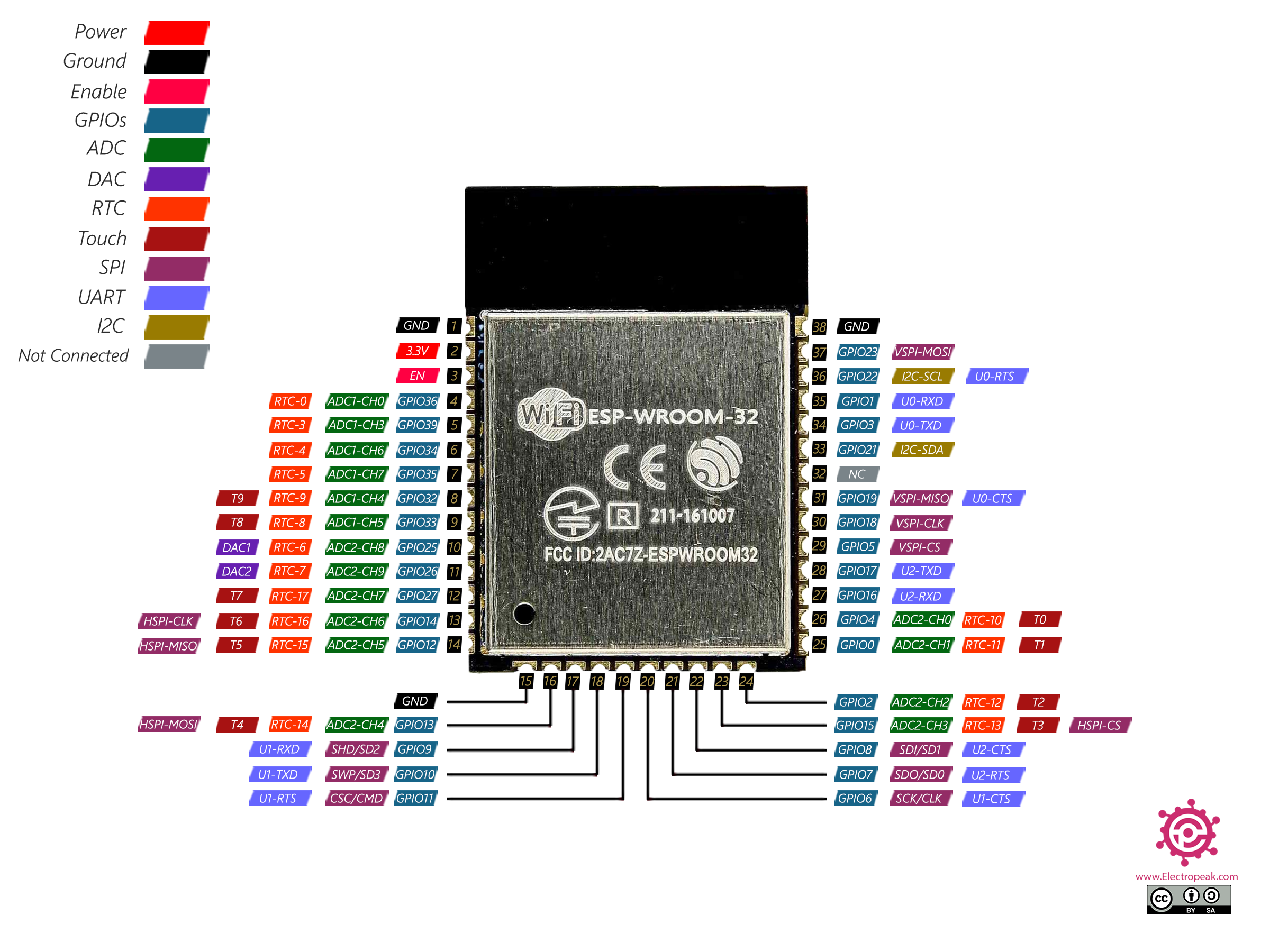
Microcontroller specifications
Before working on the design, I will check my microcontroller specifications to know what and how to make the circuit board.
Firstly, the board I chose to work with is calles an esp32 wroom 32.

I used the esp32 devkit and and arduino board to understand my connections better and use it as a refrence for my actual microcontroller

Designing process
Download KiCad
You can download kicad here
Chose which operating system you want to chose to download the file.

Circuit Sketch
I learned how the basic components are supposed to connect with the help of my local instructor.

These are the bacis connections I learned. For making an circuit, we need a few nessary components. - Microcontroller board - Switch(button)(to connect to the gnd and the en to make the reset button in the circuit board.) - Resistor(To ballence the flow of the vcc and the en) - Regulator(It converts the power supply which is 5v to 3.3v so that the esp can handel it and it won’t burn out.) - Capicator(to help the regulator with the currents flow) - Slide switch(for program run)

Download Kicad fab file
Step 1 - Search up fab library KiCad and click on the first link that pops up.

You can find the file here
Step 2 - After opening it in gitlab, than download the zip file

Step 3 - Now, open KiCad. (you should have it installedby now) and go to
Prefrences - Manage Symbol Library

Step 4 - Then, click on the bottom of the tab that shows up. There should be a folder like icon.

Step 5 - Then, when the files option shows up, go to downloads and select the fab KiCad file.

Your symbol library is now updated!
Step 7 - Now, you need to update the footprint library.Like before, go to:
Prefrences - Manage footprint Library
- Than, insted of the folder icon, select the plus(+) icon.Make sure to name the folder something thats easy to remember.

Step 5 - Then, click to the folder icon thats beside the new file you created.

Step 5 - Open the fab kicad folder to another file called fab pretty and select it.

After you select this, you are now done with updating the footprint library as well.We can now start with the actual Schematic Layout
KiCad Schematic Layout
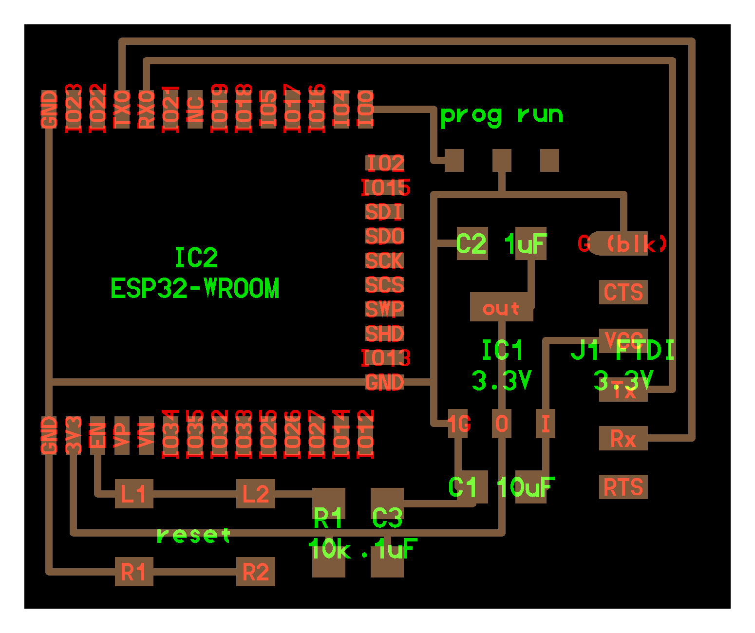
I followed the sketch I showed earler and made the circuit bellow.
Component Placement & Wiring
When placing components in KiCad, I start by adding the microcontroller, then place other components like resistors, capacitors, switches, and voltage regulators around it based on the functional blocks. I try to keep related components close together to reduce long traces.
To place components: I use the Add Symbol (a button with an op-amp icon) and search for the component I need.
To create wires: I use the Wire tool (shortcut W) to connect pins between components. I also use labels to simplify connections and avoid long crossing wires. Labels help especially when multiple wires need to connect to the same net, like GND or VCC.
Annotations: I add text notes near key connections for clarity, for example labeling which pin is for reset or IO functions.
Why Each Component is Needed
Switch / Push Button: This is connected between EN (Enable) and GND. Pressing it resets the ESP32.
Slide Switch: It allows switching the circuit between program mode (IO0 low) and normal operation. This is useful to upload code to the ESP32 without physically changing wires each time.
Resistors: Used to limit current to LEDs or provide pull-up/pull-down functionality. For example, the resistor near the EN pin ensures a stable voltage for reset.
Capacitors: Stabilize voltage and help the regulator handle transient currents.
Voltage Regulator: Converts 5V from USB or power supply to 3.3V needed by ESP32. Correction: I now connect the Vo (output) of the regulator to the 3.3V rail of the board to supply the microcontroller.
IO Pins:
Pins connected to the pin headers are used for external peripherals (sensors, LEDs, buttons).
Each pin has a label in KiCad for clarity (e.g., IO0 → programming mode, GPIO2 → LED).
- This is how the workspace looks when we open kicad and open a schematic sketch

- Now, making the circuit, to access the components we can click on the arrow icon in the toolbar like shown below.

This is the finished circuit.

Than, I started working on the pcb design.
Pcb circuit
While designing this, there were a few things that I needed to keep in mind.
Initial Placement
I start by placing the ESP32 footprint at the center of the board.
Next, I place critical components nearby: voltage regulator, reset button, slide switch, and capacitors.
Headers and pin sockets are placed on the edges for easy external connections.
Routing Challenges
Routing traces was tricky around high-density pins of the ESP32. I used different wire widths: 0.4 mm for signal GPIOs, 0.8 mm for VCC and GND.
Avoided 90° angles and crossed wires to reduce the chance of interference and short circuits.
Used labels for GND and VCC nets to simplify routing.
Basic Tools in KiCad
Add Symbol: Places components.
Wire Tool (W): Connects components.
Label Tool: Names nets to reduce messy crossings.
Rotate / Move Tool (R / M): Adjusts component orientation and position.
Design Rule Check (DRC): Checks if traces are too close or if there are missing connections.
Rules and steps
- No making 90 angle truns
- Don’t cross wires over the micricintroller board
- Don’t place the wires to close together, or it might shortcircuit.
- Change the wire sizes to keep things clear(0.4 for GPIO and 0.8 for gnd and vcc)
 (while setting predefined trace sizes helped with consistency, using Net Classes would make the design more organized and scalable, especially for projects with different current or signal requirements. I’ll try using this in the future)
- To rotate a component, click on the component and press r.
- Go to prefrences, manage footprint library to save the changes.
- While making a boarder for the finished circuit, use this tool(I was advised to make it a rectangle to keep it simple, and to be able to add my initals in inkscape.)

Keeping these in mind, I made the connections. Heres how to make the boarder for the finished circuit.
Exporting the file
Go to file- export- svg and change the settings according to your machine.


Error and Fixing
I went through a few errors while tring to access this file.The mistake I made was naming the folder instead of directing it from my laptop. This took help from a senior of mine to fix, so I wanted to advice anyone in case they make the same mistake!

Anyways, This is my first pcb design for this week!

Resizing the content in Inkscape ensures the PCB outline and traces fit exactly in the cutting area and maintain proper proportions. I resize the design content, not the F_Cu layer itself, to avoid trace distortion.
Adding initials or border: Helps identify the board after fabrication, but the actual border for cutting will be handled in the fabrication week using proper mods settings.
Notes for Fabrication (Preview)
During fabrication, I will use MODS settings for tool size, offset, and cut depth. For now, the SVG includes the outline and traces but the border is only for visual reference.
Finishing design
Inkscape
Firstly, after inkscape is opened, we have to import the design.To do this, go to file-Import.

Than, after your design shows up, we have to resize it. Press (Ctrl)+(Shift)+(D) than resize to content.

After thats done, write your initals if you want to and export(file-export) your design.
ModsCE
Now that we’re done with the inkscape design, now we can work on mods to get the cutting boarder line!
You can access mods here
Step-1 - Open mods and than right click. Select Programs-Open Program-Roland-mill 2D Pcb


Step-2 - This should have appered after the previous steps. Import the schematic layout you made from inkscape.

Step-3 - Invert the design you imported

Step-4 - Change the orgins to 0.

Step-5 - Delate a few unecessary mods

Step-6 - Right click again. Select Modules-Add modules-File-Save - Connect the new mod with the old one, and lastly click on calulate to get your circuit cutout.


Here is the finished product!

And here is my circuit board cutout!

(the toolpath generated had some errors so I changed the design file.The proper outcome will be in electronics production)
Original Design Files’
Thank you!