1. Group Assingment
The full group assignment can be found
here
For this week assignment we looked at two processes:
- Milling a board and cutting it with the CNC machine.
- Milling a board and cutting it with the CNC machine.
- Engraving the board copper paths with a Llaser machine and then cutting it with the CNC machine.
For the milling process we used the:
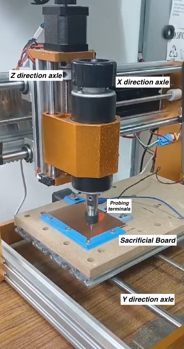
LUNYEE All-Metal 500W CNC Router Machine
Specifications:
- Working area: 300x180x80mm
- Machine size: 485x415x374mm
- Spindle: stnd configuration: 500W 10000 r/min
- Machine accuracy: +/- 0.1mm
- Max speed 5000mm/min
- Max cutting speed 2000mm/min
- Power supply 48V 500W
This machine is suitable for milling: wood,bamboo,acrylic,plastic, PVC, ABS, PCB, brass and resin.
In general terms, the machine consists of three axes that allow the milling bit to move in three directions. It features two pole terminals (positive and negative) used to determine the probing depth. One terminal is connected to the milling head, while the other is attached to the board. When the tip of the bit touches the metal plate, it completes an electrical circuit, allowing the machine to record the exact depth of the board surface.
Below we can find some safety guidelines:
- Be aware where the stop button is.
- Use appropriate goggles when operating the machine.
- Use appropriate breathing protection given the material you are cutting.
- If you have long hair tied it back.
- Do not use gloves as they can get caught in the spindle.
- Ensure proper ventilation
- When changing bits disconnect the machine.
- Make sure clamps are well fastened.
- Make sure there is no wiring in the cutting area for example remove the probes terminal before cutting.
- Double check that you have the right cutting area.
- Stay close by the machine while there is a ongoing cut job.
For engraving in the second process we explored we used the following laser engraver.
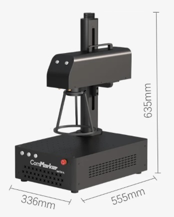
ComMarker B4 MOPA 60
An additional but important accessory of the laser is a safety enclosure that is made of an anti laser coating light absorbing material.
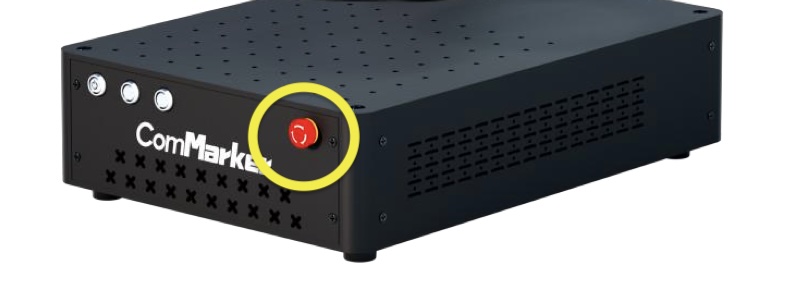
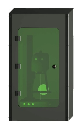 Please note that once the engraver is enclosed, the emergency stop
button (highlighted in yellow) will not be accessible from the outside.
Ideally, an additional emergency stop button should be installed on the
exterior of the enclosure for safety and easy access.
Please note that once the engraver is enclosed, the emergency stop
button (highlighted in yellow) will not be accessible from the outside.
Ideally, an additional emergency stop button should be installed on the
exterior of the enclosure for safety and easy access.
Specifications:
- Laser Source: MOPA-JPT
- Laser Power: 60W
- Laser Wavelength: 1064nm
- Engraving Accuracy: 0.01mm
- Engraving Speed: 0-15,000 mm/s
- Frequency 1-4000 KHz
- Pulse Width: 2-500ns
- Work Area: 110mm x 200mm dual lenses
- Primarily designed for engraving metals and plastics
- Can cut Stainless Steel, Aluminum, Brass, Copper, Silver and Gold.
In this page you can find a blog that describes the advantages that a fiber laser engraver have for PCB engraving. Below you canfind a short summary of this article.
The high precision laser technology of a fiber laser engraver allows to etch, cut and mark the different layers of a printed circuit board. Some specific advantages are:
- High Precision and Accuracy to achieve fine detail.
- Efficiency and Speed resulting in faster processing than traditional methods thanks to high speed galvo technology.
- Versatility: that allows processing several types materials.
- Auto Focus Technology: Allows adjustments based on material thickness and variations in the material surface.
This is a laser cutter that uses the MOPA technology i.e Master Oscillator Power Amplifier. This technology has a much wider frequency range than q-switch machines and it can also control the pulse width parameter enabling the control of the individual laser pulses.
In the fields of Electronics, Semiconductors, and ITO Precision Machining achieving precise lining is often essential. However, a Q-switched fiber laser struggles with this task due to its fixed pulse width. In contrast, a MOPA fiber laser, with its adjustable pulse width and frequency, effectively delivers smooth edges and precise results. Mopa Fiber laser has a tunable width which facilitates small laser spot and tunable energy (source: link)
Steps for engraving a PCB:
- Design Circuit Diagram
- Input the Circuit Diagram into EZCAD in our case we have a version of Lightburn.
- Set Parameters power, speed, and frequency
- Preview and adjust position and size
- Initiate the laser engraving process.
- Check the result.
Safety
These are additional safety guidelines that complement those outlined in Week 3, as this is a powerful and potentially dangerous machine. The following points are excerpted from the manual:
- Laser Safety
- The machines use Class IV lasers. The lasers are very powerful and can cause eye injuries and burnt kin. It is recommended to wear laser goggles when using the laser engraver.
- Avoid exposing your skin to Class IV laser beams, especially at close range.
- Do not touch the laser engraving beam while it is switched on.
- Material Safety
- Do not engrave materials with unknown properties.
- User Safety
- Use this laser engraving device only in accordance with all applicable local and national laws and regulations.
- Use this device only in accordance with this instruction manual and engraving software manual.
- DO NOT leave this device unattended during operation.
- Cut off all power to the machine and contact either our customer service or repair service if anything seems to be working abnormally.
- Be aware that where the
- Any untrained personnel who might be near the device must be informed the danger of the machine before operation
Milling/Cutting Materials for Electronics
Finally, it is important to metion some characteristics of the material we used (FR1) and the FR4 another commonly used material. Below you can find a summary from link by ChatGPT on the advantages and disadvantages of these materials (prompt: please summarise this in 2 paragraphs )
FR1 and FR4 are two commonly used materials in PCB (Printed Circuit Board) manufacturing, each with distinct compositions and properties that suit different electronic applications. FR1 is a paper-based material impregnated with phenolic resin, known for its low cost and ease of machining, but it offers lower mechanical strength, thermal resistance, and electrical insulation. In contrast, FR4 is made from woven fiberglass cloth and epoxy resin, providing superior strength, higher heat tolerance, and better electrical properties, making it more suitable for demanding electronic environments.
The choice between FR1 and FR4 depends on the specific requirements of the application. FR1 is typically used for low-cost, single or double-layer PCBs where performance demands are modest. On the other hand, FR4 is favored for multilayer PCBs and high-performance electronics due to its robustness and reliability under stress and heat. Understanding these differences allows engineers and designers to select the right material for optimal functionality and cost-efficiency in their electronic projects.
Finally, it is important to emphasize that FR4 can be a much more dangerous material to work with especially if aspired as it is fiber glass based.
Generating files in Kicad
This week, our goal was to simulate the process of sending a printed circuit board (PCB) design to a manufacturer. To achieve this, we needed to generate Gerber files—essential documents used in PCB production.
To create the Gerber files, we followed these steps:
- Navigate to the File menu and select Plots.
- Configure the production settings according to the specifications of our chosen manufacturer.
For a concise demonstration of how to format Gerber files specifically for NextPCB, refer to the video linked below.
Generating Gerber Files in KiCad
KiCad 9 has introduced several interface changes, which might make it
tricky to locate certain options. If you’re starting with the default
settings for generating Gerber files, you can navigate to File →
Fabrication Outputs → Gerbers. 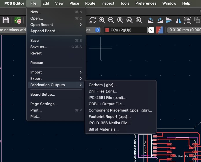
From there, you can use the default layer selections and settings provided by KiCad or you may want to modify if you know the correct settings.
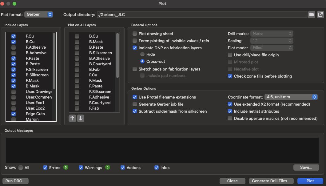
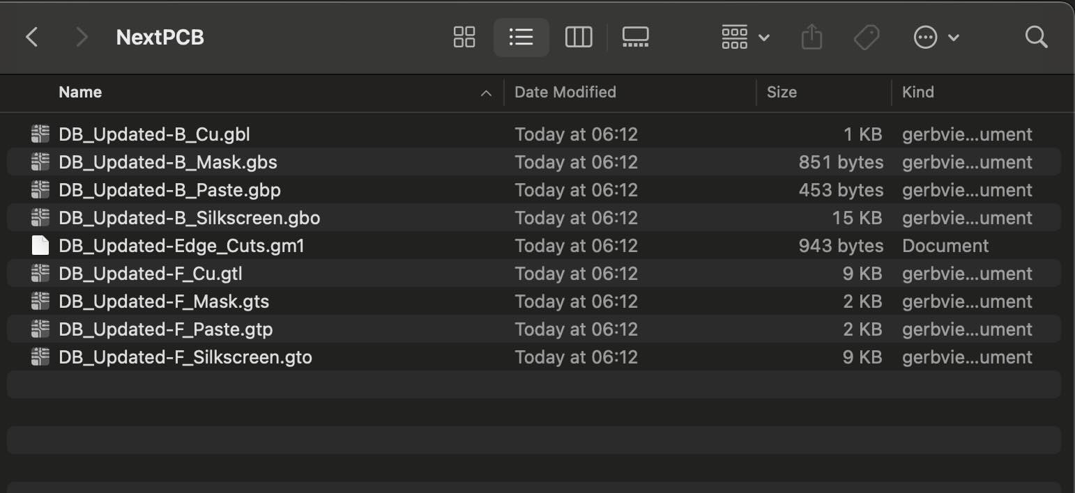
As per the video above we use the defaults and select use protel file name extension. In addition, create a dedicated directory to store your output files, as they can quickly become disorganized. Once the directory is set, press “Plot” and your files will be generated in the specified location.
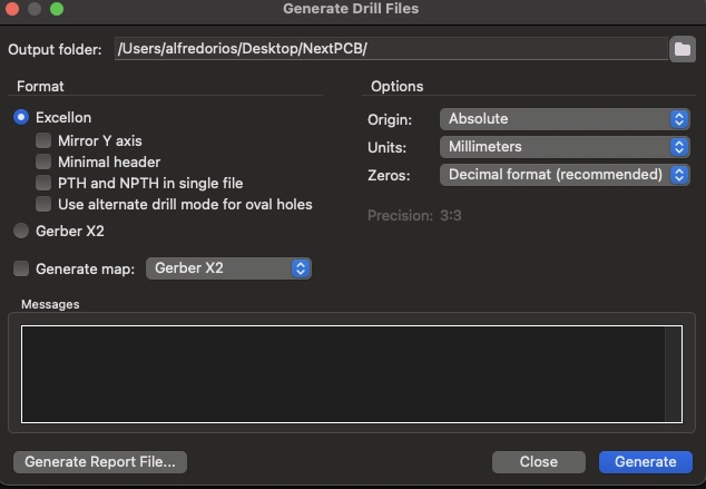
Next, press “Generate Drill Files.” This step is useful if your PCB requires holes to be drilled—for example, for mounting purposes.
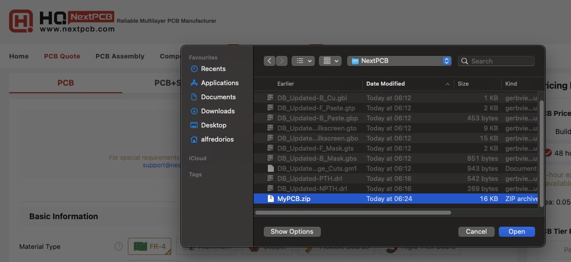
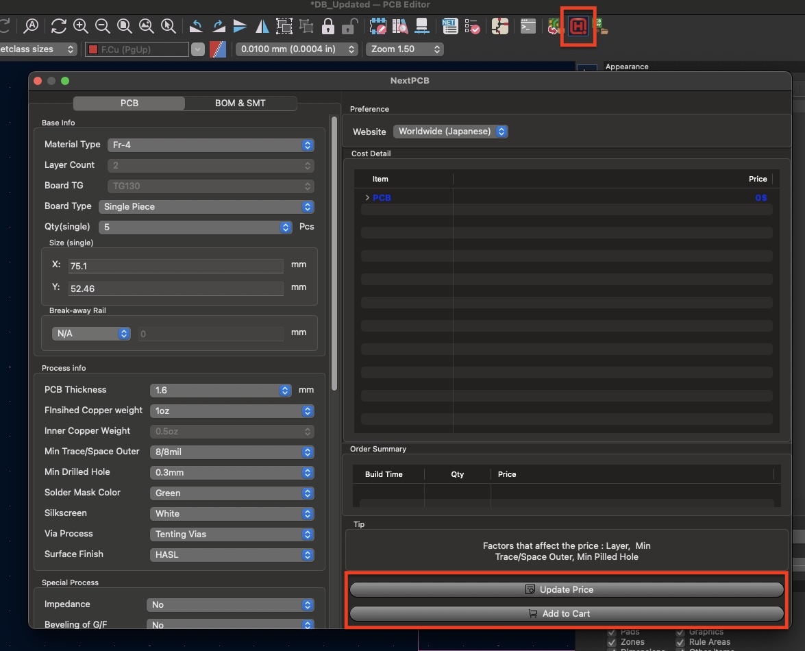
Thereafter, you will need to generate the zip file with all the files created in order to upload them to NextPCB page that you can see below.
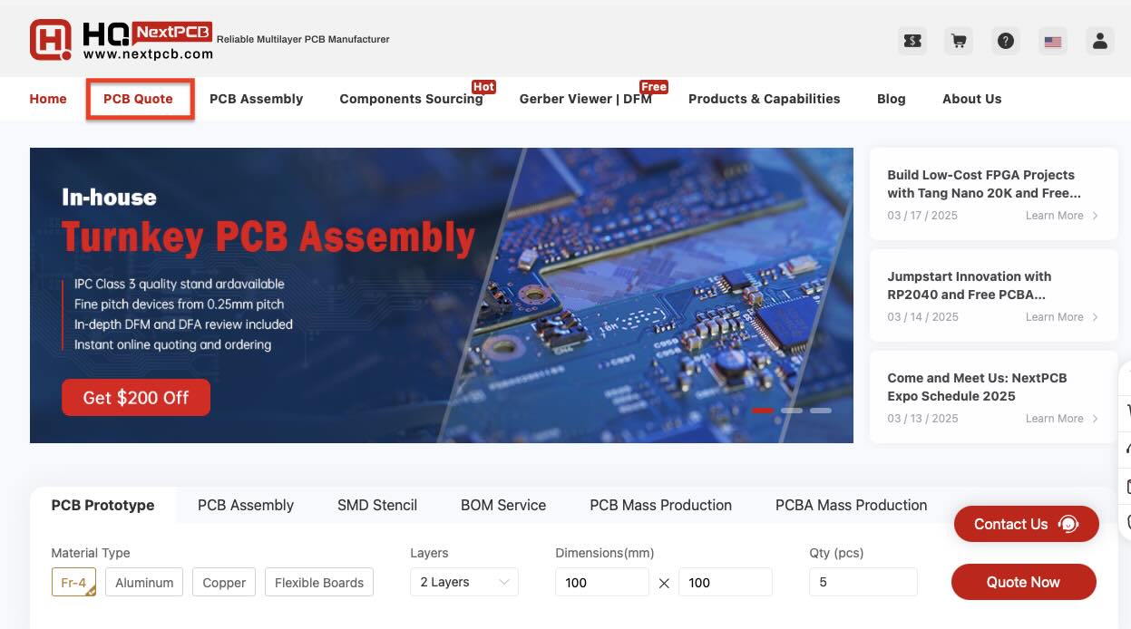
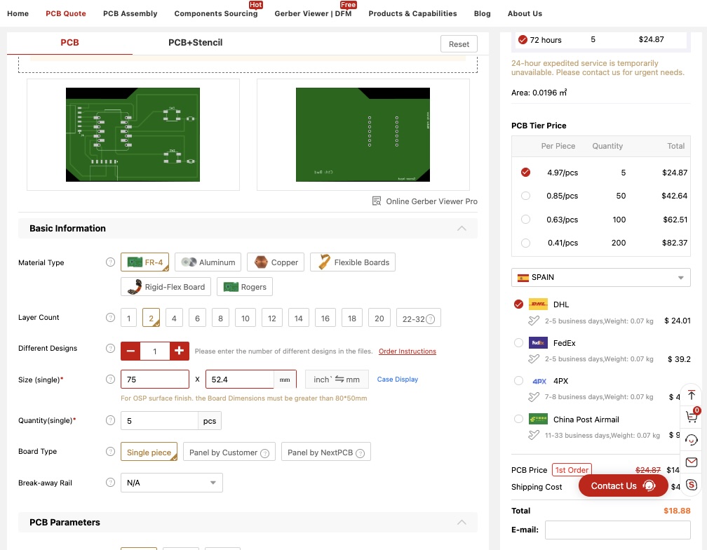
Here you can see the different options chosen and the price of the boards and shipping resulting from the uploaded files.
Alternatively, using a plugin can streamline the process. For example, plugins tailored for specific manufacturers, like NextPCB, can automatically configure the settings to match their requirements
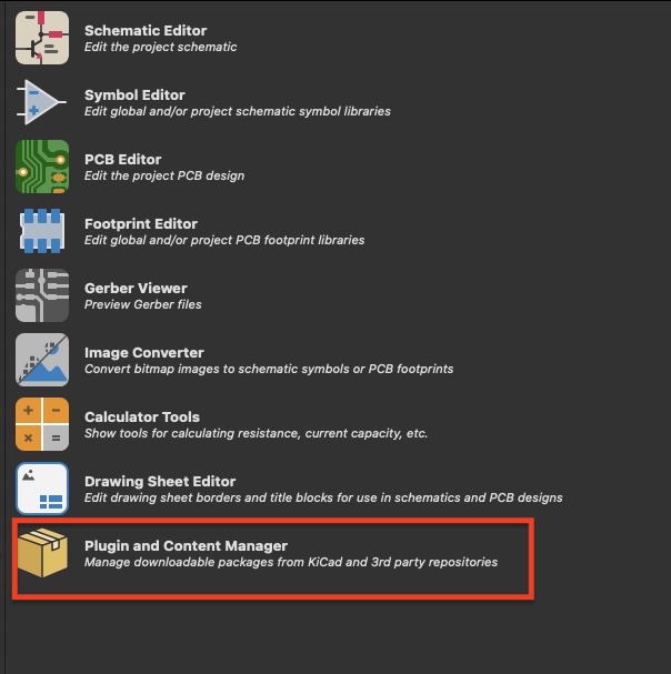
Once the plugin is installed, it can be accessed directly from the menu to review the configuration options provided by the company. This ensures that all necessary parameters for production are properly set. After verifying the options, you can click “Update Price” to receive an instant quotation for the board. If you’re satisfied with the setup and pricing, you can proceed by selecting “Add to Cart”, which will redirect you to the company’s website to finalize your order, just as before.
Happy ordering!
Individual Assignment
Board design and milling/Engraving
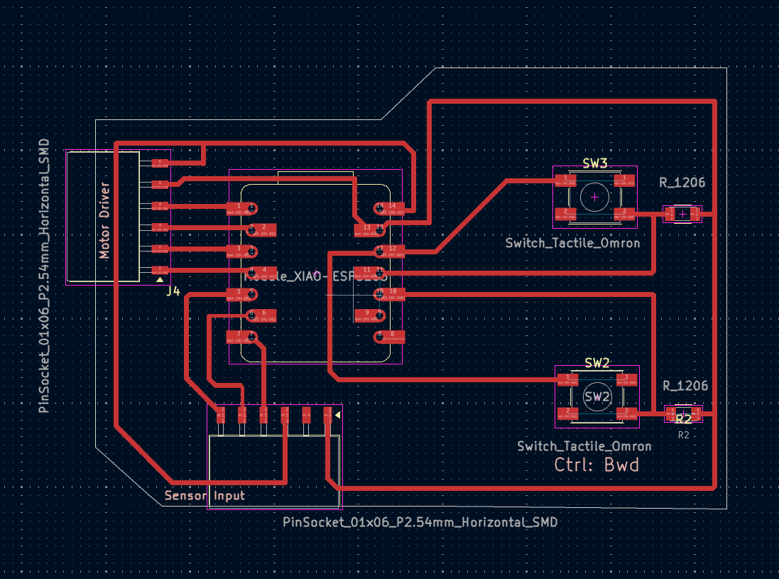
A goal for this week was to create a PCB for this purpose I used the board I designed in the electronic design week. Basically the goal of this board is to use it to test an half bridge to use a DC motor.
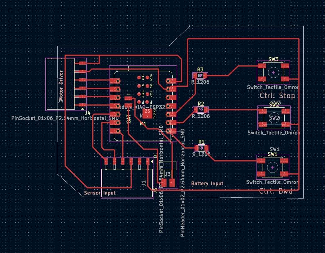
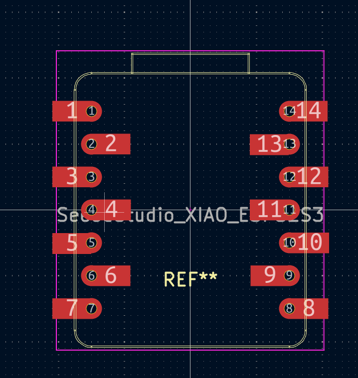
I had to do modify the board as I wanted to mount the micro controller on the board as a removable piece (soldered to a socket) and for this there were only pins that alternated from one side to the other.
In order to do this I did a quick fix by modifying the the micro controller footprint from the foot print editor. Note: this is not ideal better to find the right component. I moved the position of the Xiao board pads to fit the header pin feet.
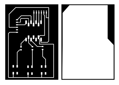
Then, I proceeded to generate some gerber files and used the Png to Gerber online app tool from fab lab Kerala
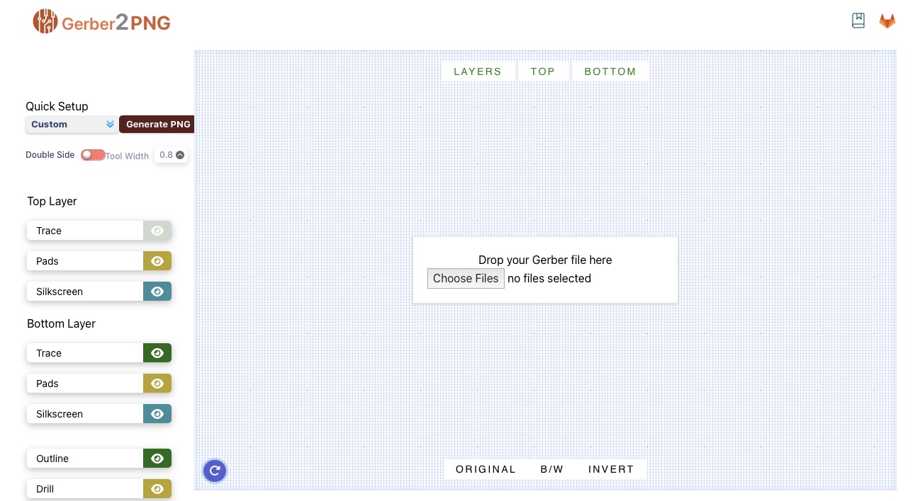
And produced two files one for cutting and the other one for the traces.
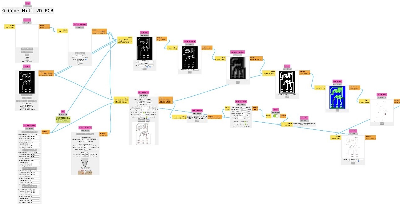
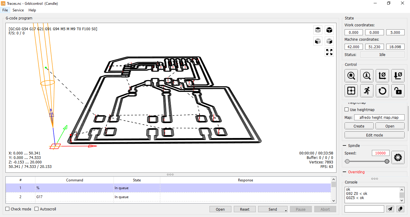
Therafter, in Mods I generated the two corresponding Gcode files. Basically, these files will create the parameters needed for cutting and the paths that the milling/cutting tool will follow.
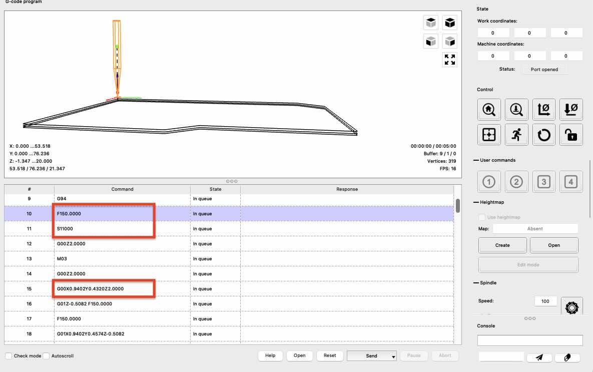
After generating the necessary files, I imported them into Candle.
You can download Candle for Mac from the following website: 👉 https://bachinmaker.com/?p=73
When using Mods, the software generates a G-code file. This file contains essential instructions for your CNC machine, including:
- Feed and spindle speeds
- XYZ movement paths
These instructions are based on the parameters you input into Mods. Each cell in the interface displays what the G-code is doing at each step. In our cutting file for example:
- The spindle speed is set to 11,000 RPM.
- Note: Candle limits the maximum speed to 10,000 RPM, which also happens to match the maximum spindle speed of the machine.
- The feed rate along the board outline is 150 mm/min (approximately 2.5 mm/s).
- The G-code also shows the precise XYZ coordinates that the cutting bit will follow.
Further inspection of the cells indicate the maximum cutting depth was 1.35 mm Intermediate depths were set at 0.5 mm and 1.0 mm The board thickness is 1.3 mm. This setup ensures the cutting process goes slightly beyond the board thickness, guaranteeing a complete cut through the material.
One can find the specific codes in the following wiki site.
https://github.com/gnea/grbl/wiki
Similarly, for the tracing we had the same values in spindle and feed speeds and a depth of 0.15 mm.
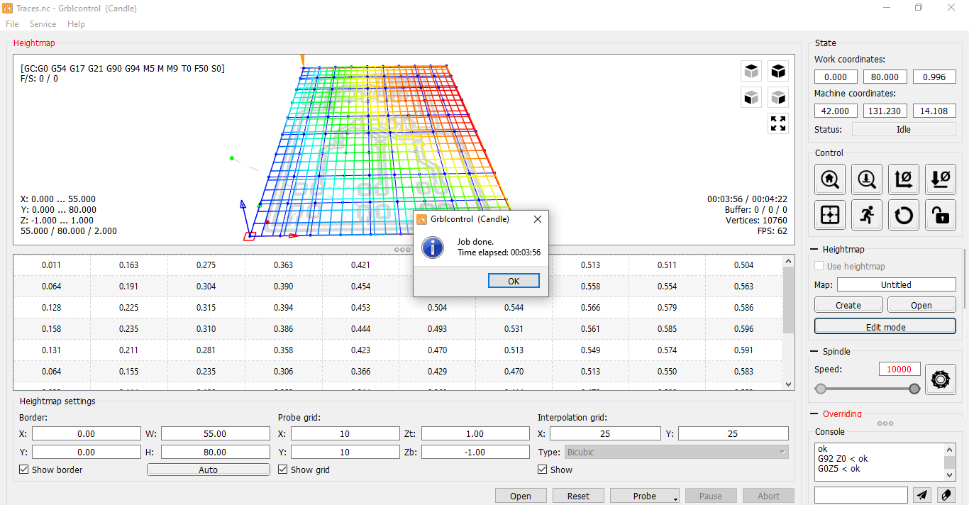
I used Candle to generate a height map, which helps the machine compensate for PCB bowing caused by clamping, as well as any thickness irregularities resulting from the manufacturing process.
Note: To generate the height map, the relevant G-code file must be opened in Candle.
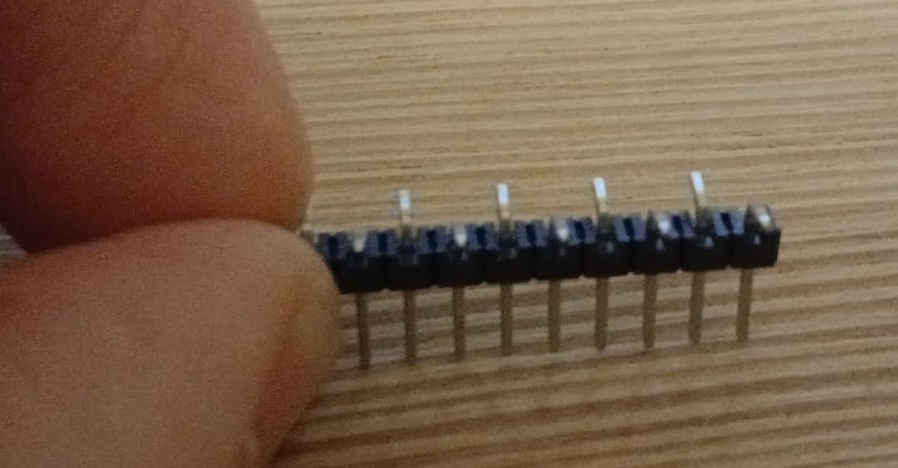
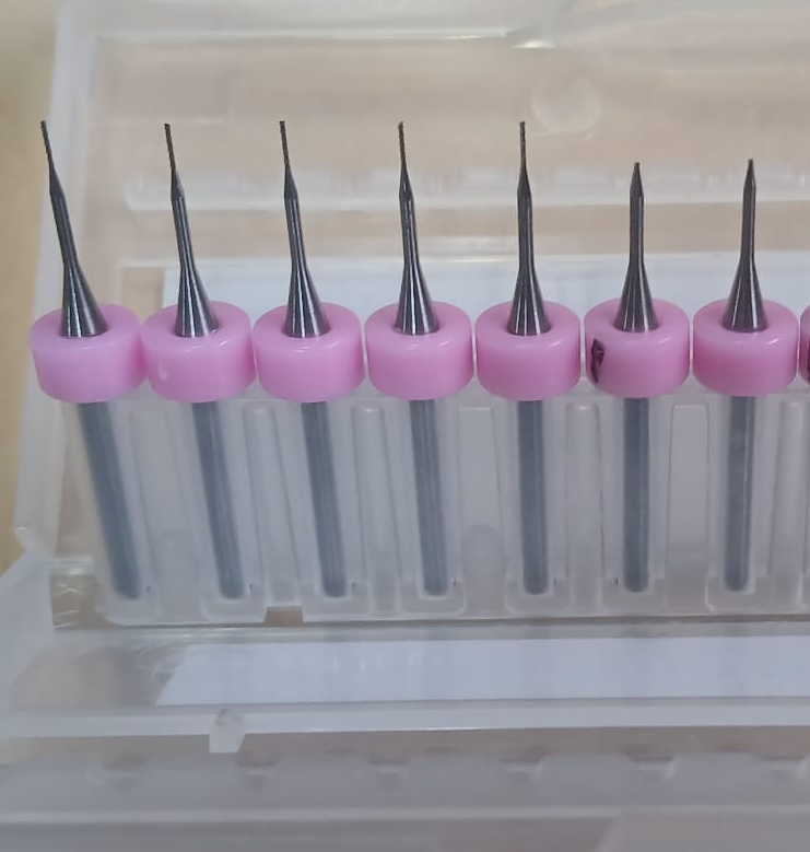
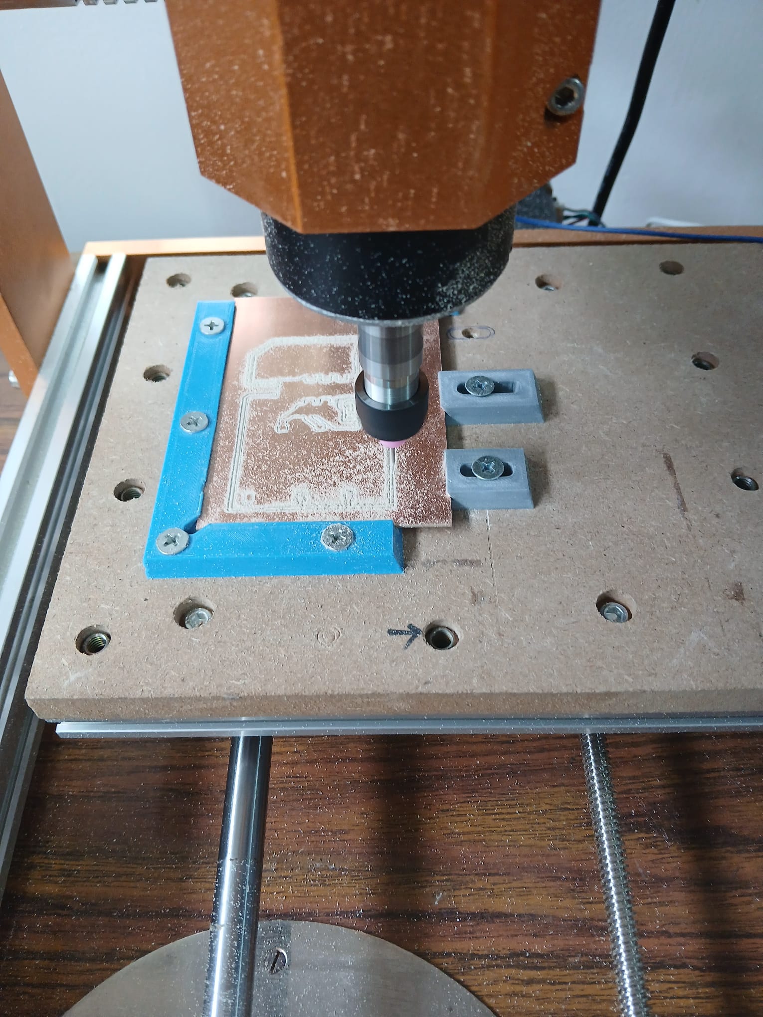
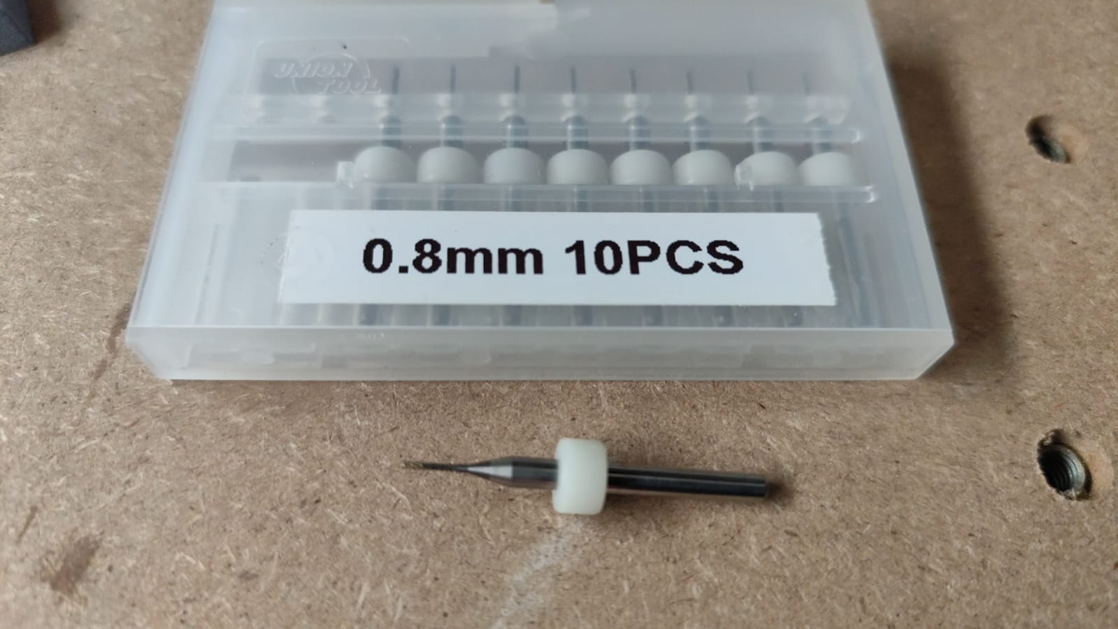
And then I sent the job for tracing. For this we used a 0.4 mm flat end bit. While tracing the board, I broke 2 flat end mill bits that you can see below.
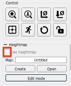
First, we thought the problem was the feed speed so we reduced it. but later I found out that I had not checked the height map option.
After this modification we found that no more problems but the job took more than an hour as I did not increase the feed speed (40%) just in case as we had already lost a bit of time.
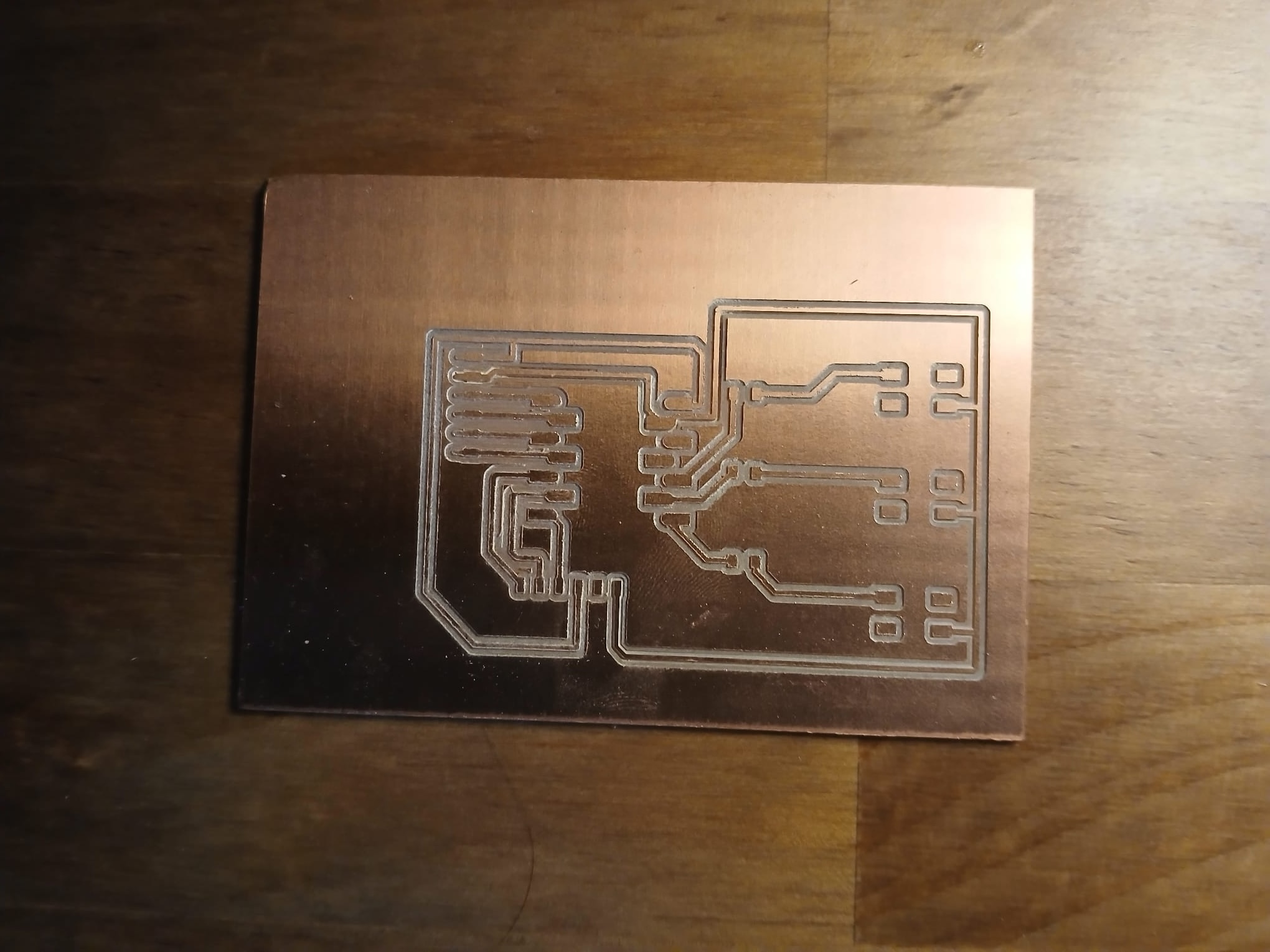
Below you can find the final board.
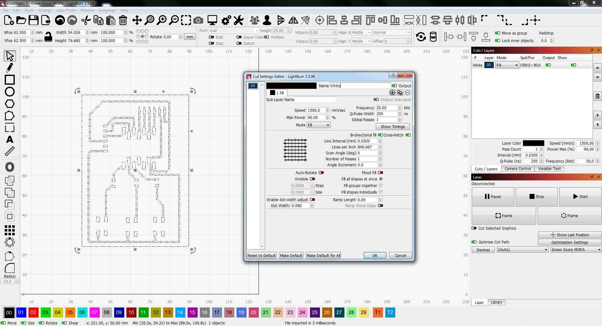
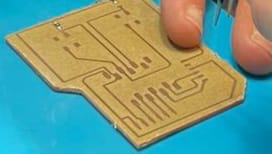
Thereafter, I used the ComMarker B4 MOPA 60 laser engraver in order to do the traces i.e. to test the second process. I imported an svg file to the Lightburn software which you can see below.
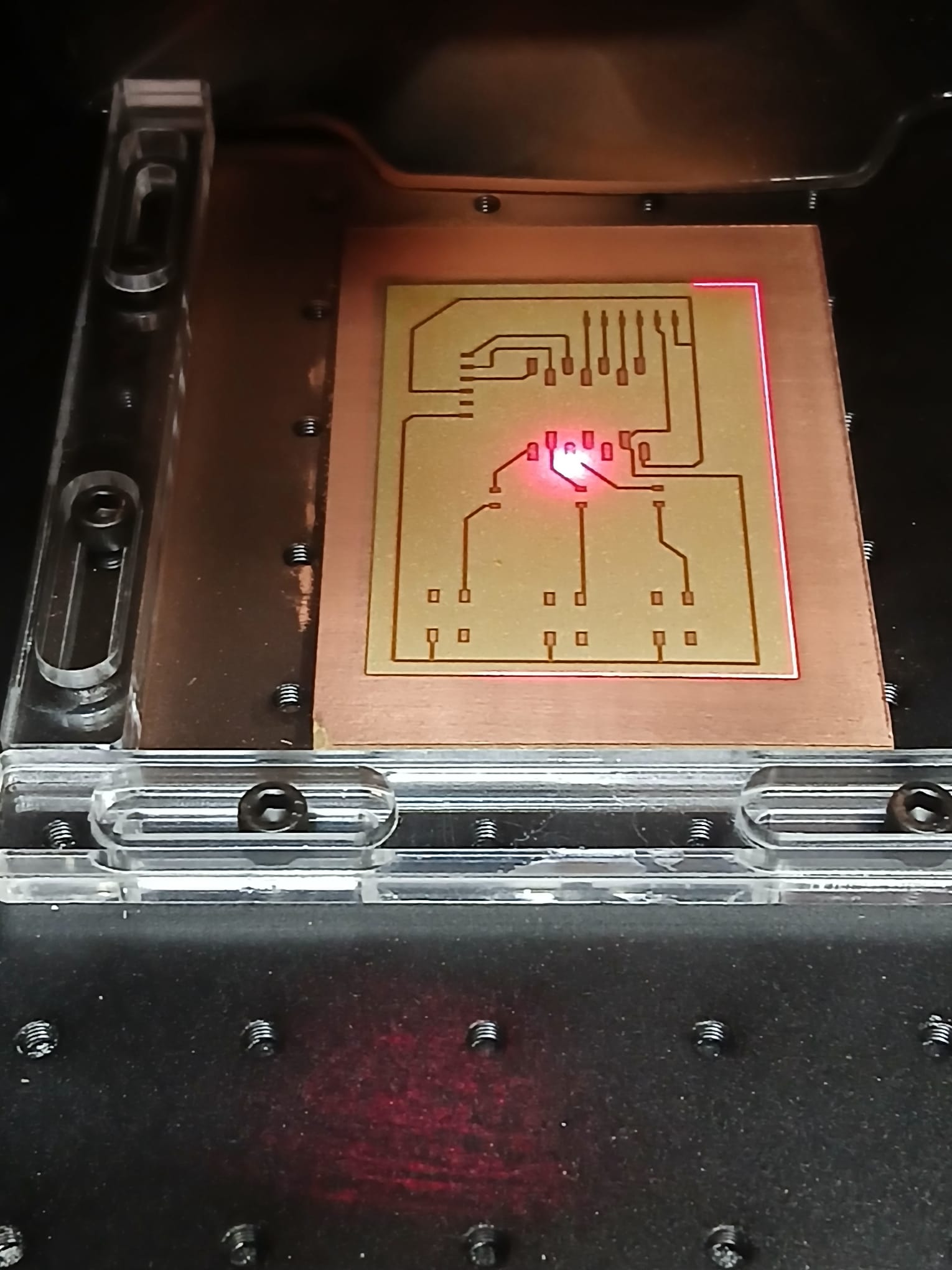
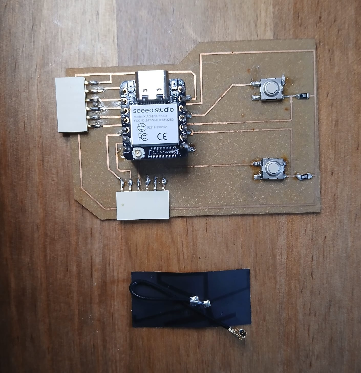
And here you can see the finished board:
Board correction
After engraving the board, I realized that there was a mistake in the board I designed first, this design is OK for a board with a micro controller that has pull up resistors, if that is the case the case the resistor I placed would have been redundant. I still was not quite sure if this micro controller had this capabilities. So, I modified my board and simplified it a bit and used a pull down resistor. The resulting design can be found below.
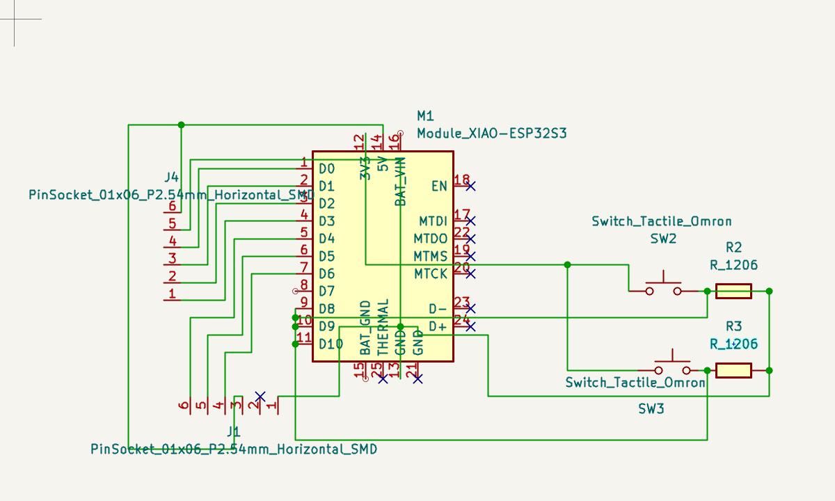
The components needed for the board can be found in the table below.
| Component | Code | Units |
|---|---|---|
| Resistor | R1206 (1k Ohms) | 2 |
| Button | Omron B3SN | 2 |
| Pinsocket | Pinsocket 1x6 P2.54mm horizontal SMD | 2 |
I cut the board I produced using the laser engraver with a power setting of 90% and 4 passes. The board was then cut using a 0.8 mm flat end mill bit.
In the rush on Friday, I forgot to take pictures of the final “naked” version of the board. However, I did find one that shows the board with only the resistors. After engraving and milling the board, I proceeded to solder the components.
Soldering
Soldering is a technique used to join two metal surfaces using a filler metal, commonly referred to as solder. This filler metal is often made from alloys such as tin-lead or tin-copper. In addition to the type of solder used, temperature plays a crucial role in the process, as different solders melt at different temperatures. Applying heat must be done carefully—insufficient heat can result in weak joints, while excessive heat may damage the components being joined (Wikipedia).
The amount of heat is required depends on the thermal mass of the material
\[ Q = C_{th} \Delta T \] Where Q is the thermal energy transferred, \(C_{th}\) is the thermal mass of the body and the \(\Delta T\) is the change in temperature.
This was my first time soldering components, and it was definitely an experience. To prepare, I had watched a few videos beforehand, and on Friday night, Mickael gave me a hands-on demonstration of how to solder properly. The soldering process is well exemplified in the graph below:
- Position your components
- Heat the joint,
- Solder the joint
- Inspect.

This image also illustrates the various mistakes in soldering.
Mickael also shared several helpful tips with me: use a small tip and thin solder wire for small components, prime the soldering tip with a bit of solder, and clean the tip regularly. He also showed me a useful trick—fixing one leg of a component first makes soldering the remaining points easier since the component stays in place.
Additionally, he mentioned that using flux can really help. Flux is a chemical compound that removes oxides from metal surfaces and improves solder flow, making the whole process smoother. Finally, he also mentioned that is useful to solder first the smaller components and later the larger ones.
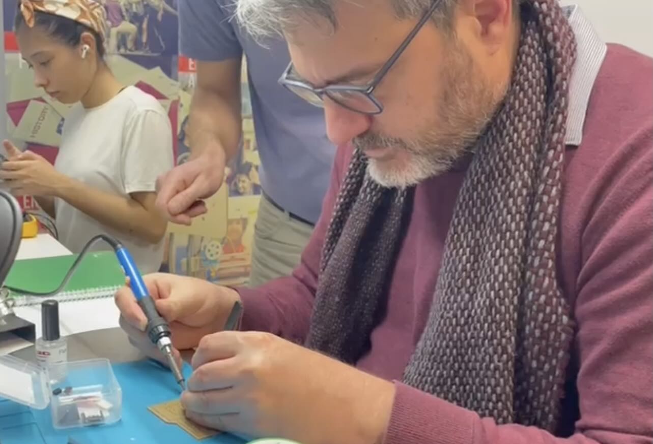
I took the board and components home with me, and over the weekend, I practiced on a couple of failed boards. Later, I tried assembling the final board. While I believe there’s still room for improvement, I was pleased to have successfully attached all the components.
“Alfredo from the future” would tell “Alfredo from the present” that the pins did not get enough soldering material.” See assignment 10.
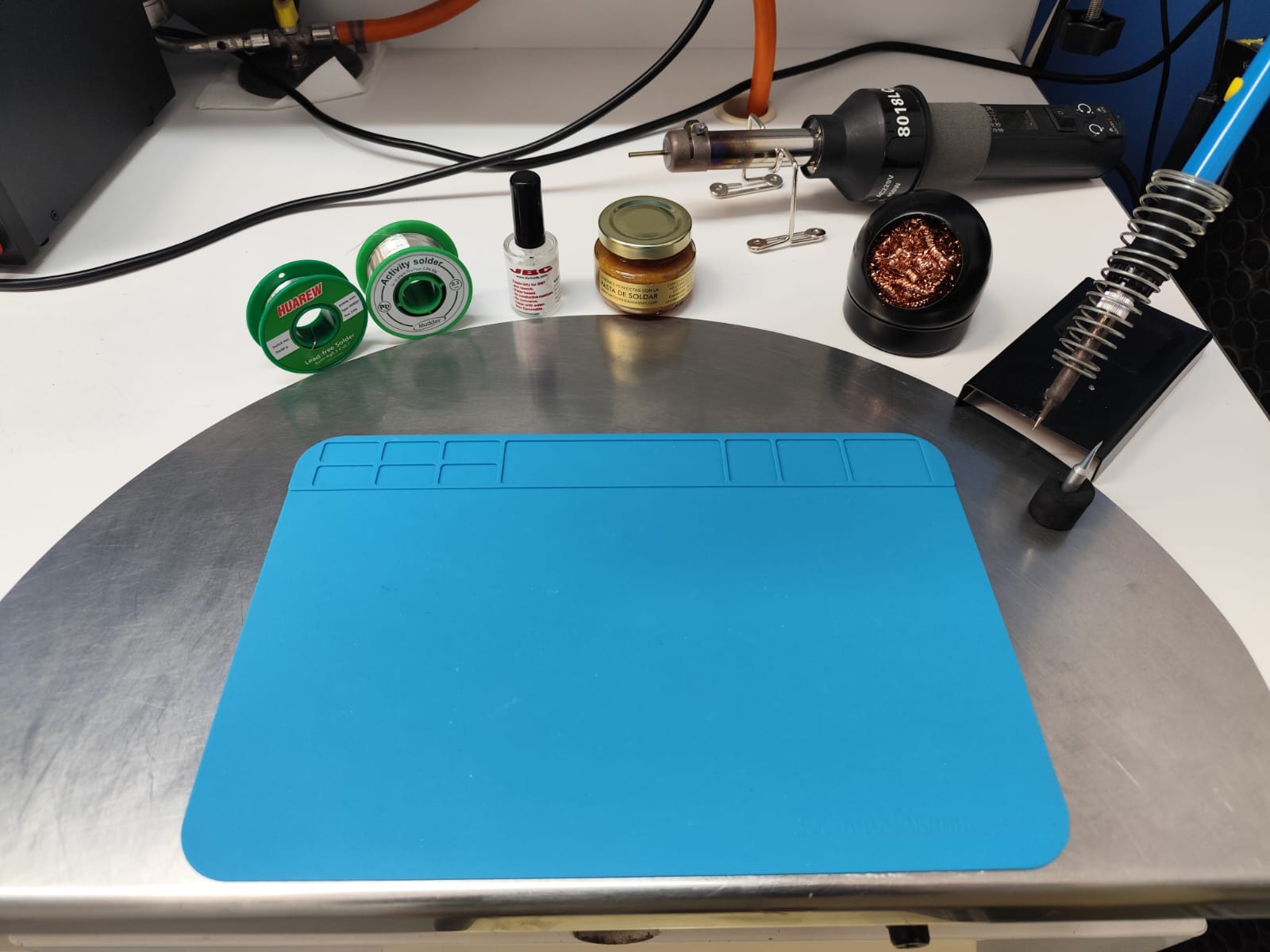
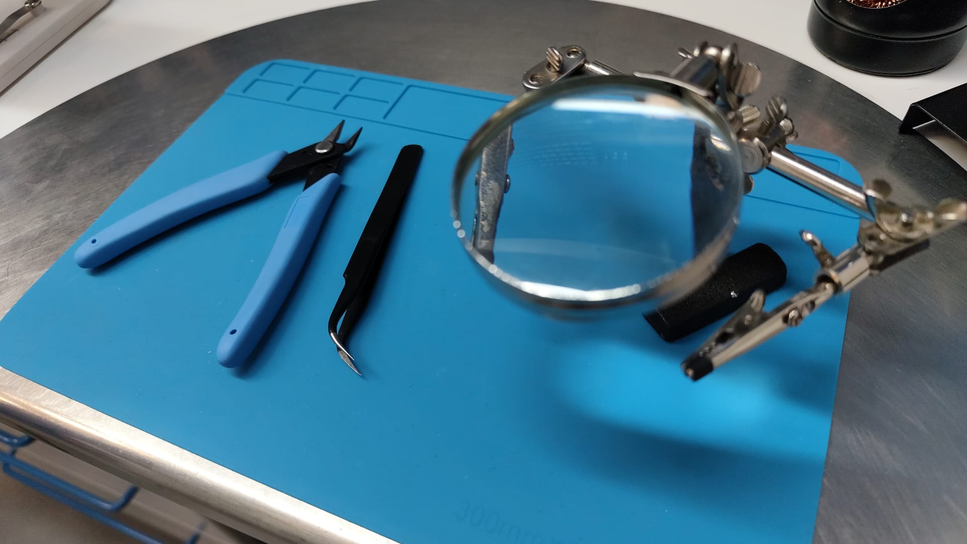
Some tools that made the soldering process easier included a silicone mat for organizing and placing components, which helped keep the workspace tidy and reduced the risk of losing small parts. In the picture, we can see a soldering iron, solder wire, flux, and a small container with a metallic sponge used to clean the soldering iron tip.
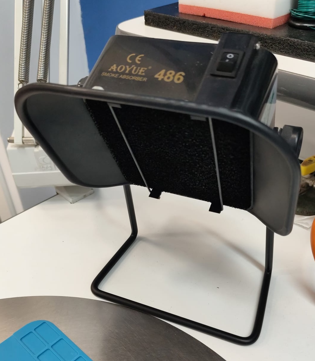
An air extractor to remove soldering fumes, which helped maintain a cleaner and safer working environment.
A magnifying glass with built-in clamps to hold the PCB in place—great for both stability and visibility when working with small components. In the picture we also see cutting pliers which can be useful for example to strip plastic. Also forceps to help manipulate small components.
Testing
Finally, I decided to test the buttons on the board I made:
from machine import Pin
import time

buttonA = Pin(8, Pin.IN)
buttonB = Pin(9, Pin.IN)

while True:
    if buttonA.value():
        print("A pressed")
        time.sleep(0.5)
    if buttonB.value():
        print("B pressed")
        time.sleep(0.5)
And they behaved adequately, with no interference.
Key learnings from this week:
- Using a laser engraver significantly sped up the process and proved to be very useful for quick prototyping.
- Soldering skills are essential for PCB development and require a lot of care and precision to avoid damaging components.
- Nowadays, sending boards to manufacturers has become incredibly easy, making the prototyping and production process much more accessible.
Evaluation
Learning outcomes:
- Described the process of tool-path generation, milling, stuffing, de-bugging and programming
- Demonstrate correct workflows and identify areas for improvement if required
Have you answered these questions?
- Linked to the group assignment page
- Documented how you made the toolpath
- Documented how you made (milled, stuffed, soldered) the board
- Documented that your board is functional
- Explained any problems and how you fixed them
- Uploaded your source code
- Included a ‘hero shot’ of your board