- group assignment: - use the test equipment in your lab to observe the operation of a micro controller circuit board
- individual assignment:
- use an EDA tool to design a development board that uses parts from the inventory to interact and communicate with an embedded microcontroller
- extra credit: try another design workflow
- extra credit: design a case for it
Group Assingment
The full group assigment can be found at this link.
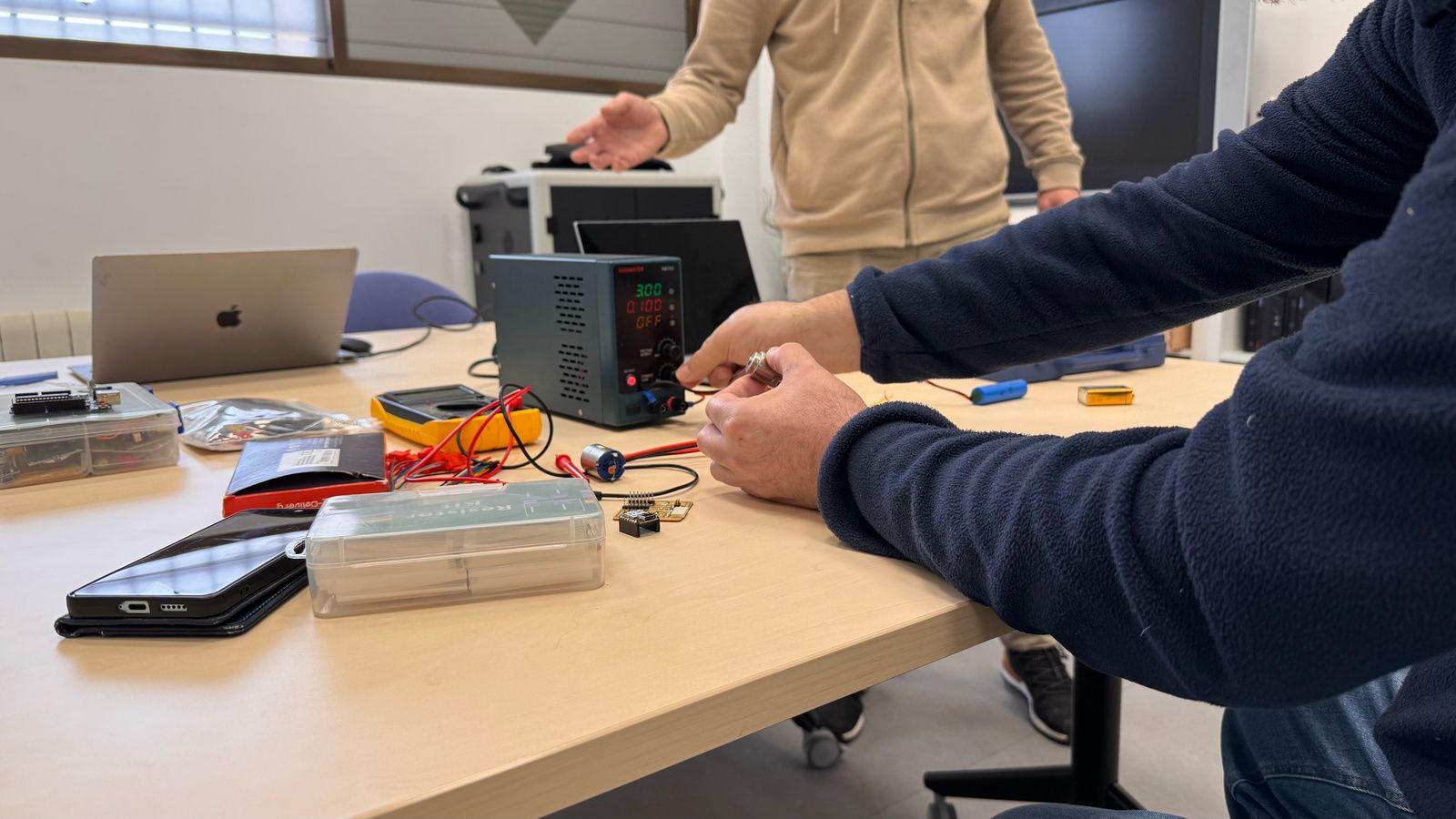
This week we got familiar with different different equipment in the lab specifically we looked at:
- the multimeter
- the logic analyzer
- a power suppy and
- the oscilloscope.
Oscilloscope
While a multimeter provides a single, averaged measurement of a signal at a given moment, an oscilloscope dynamically displays how an electrical signal changes over time.
In this video, you can observe how the signals behave as we switch from DC to AC.
To demonstrate this, we run a MicroPython program that toggles a pin on the Xiao ESP32S3 microcontroller on and off.
from machine import Pin
from time import sleep
on_pin = 4
pin = Pin(lon_pin, Pin.OUT)
for i in range(1200):
  pin.on()
  sleep(1)
  pin.off()
  sleep(1)
  print("on",i+1)
In the video above, the bottom labels on the oscilloscope display indicate the following:
- The vertical scale, showing the voltage per division on the vertical axis (in this case, 2 volts/div)
- The probe attenuation setting
- The horizontal scale, representing the time per division on the horizontal axis (in this case, 5 μs/div)
- The type of signal being measured (AC or DC coupling)
The next video gives a quick tour of the oscilloscope’s features (Spanish audio).
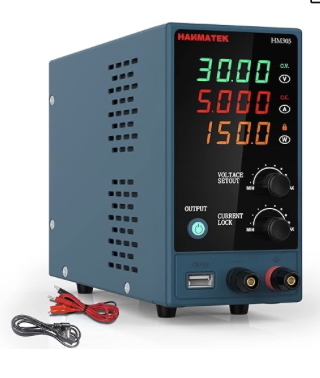
Power Suppy
The Hanmatek 305 is a power supply equipped with two knobs to control voltage and current, within a range of 0–30 volts and 0–5 amperes, respectively. It also features a safety button that stages changes made to the knobs before applying them. We used this device to power motors of different sizes, adjusting the voltage and current to estimate their operating ranges.
Individual Assingment
I wanted to design a Printed Circuit Board (PCB) that would allow me to test the various peripherals I plan to use for my final project.
Development board
Module 1: Interface to motor
The configuration of the development board will depend on what I intend to test. In my case, one important output is the rotation of a DC motor, which is used to roll the used tape in the smart trap. I would like to test the motor by changing its speed and possibly its rotation direction.
For motor control, I will use a half-bridge driver. Therefore, it is important to provide both data and power connections as inputs to the motor driver. Below is a picture of the motor driver I plan to use, with annotations indicating the function of each pin.
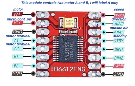
I will need routing for the following inputs: STBY, PWMA, AIN2, and AIN1, which will require 4 data pins, in addition to VCC and GND.
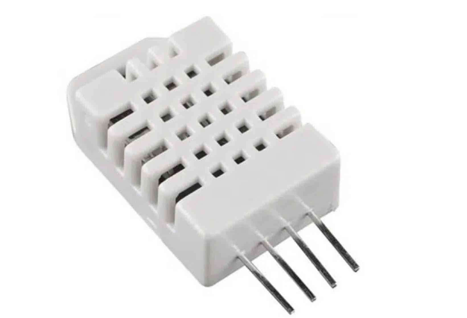
Module 2: Interface to sensing equipment
For the temperature and moisture sensor, I will use three pins: PWR, GND, and data. However, it might be useful to have additional data pins available in case we want to connect output devices, such as an OLED display, to show values when we are not connected to a computer.
Module 3: Control Buttons
This third module would include buttons to decrease and increase the motor speed. Therefore, at least two data pins, along with connections to PWR and GND, will be required. Ideally, these buttons would be somewhat separated from the rest of the board.
Pull-up and Pull-down Resistors
- In a button energy can bombard a pin that is floating which can produce random high and low voltage values.
- Adding a 10 k resistor will pull up 5v.
- If one pushes the button the microelectronic sees 0 otherwise it sees 5
- Some micro controllers have already built resistance
- Pull down to ground or pull up to a voltage supply
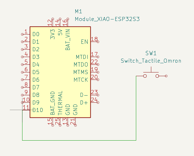
Xiao ESP32S3 sense
Here you can see the back of the card, where we find BAT+ and BAT-, which are the terminals for connecting a battery.
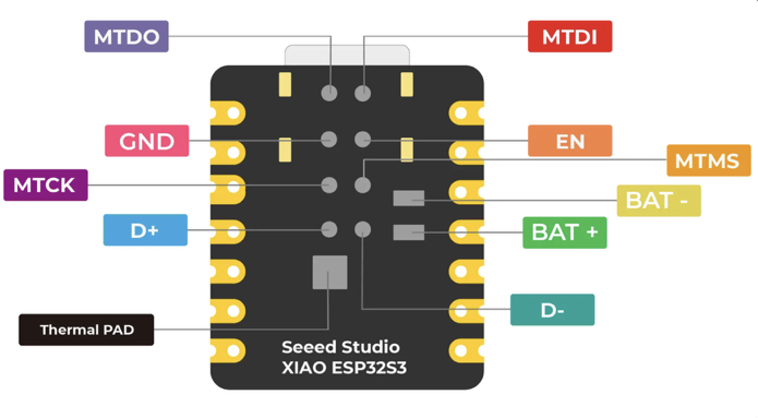
And here’s the front of the board. Note that I have not included the camera portion of the board.
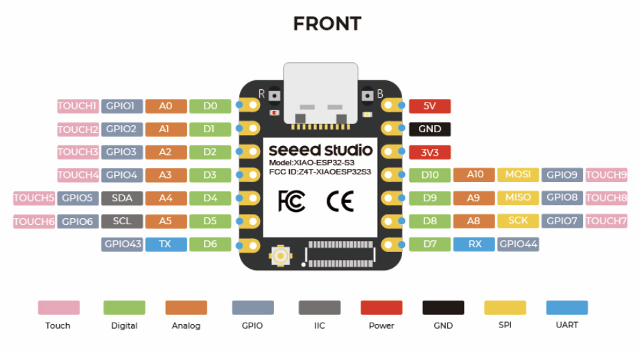
Therefore, it is important to account for all the pins that will be necessary in our KiCad design.
| Module | Ctrl | E | Pin |
|---|---|---|---|
| Motor driver | 4 | 2 | D0 D1,D2,D3 |
| DHT22 or other | 3 | 2 | D4, D5, D6 |
| Buttons | 2-3 | 2 | D7, D8 |
| Battery charger | 0 | 2 |
The assignment is limited to components to the inventory. These components ideally will be in the Fablab Eagle and Kicad libraries
Kicad
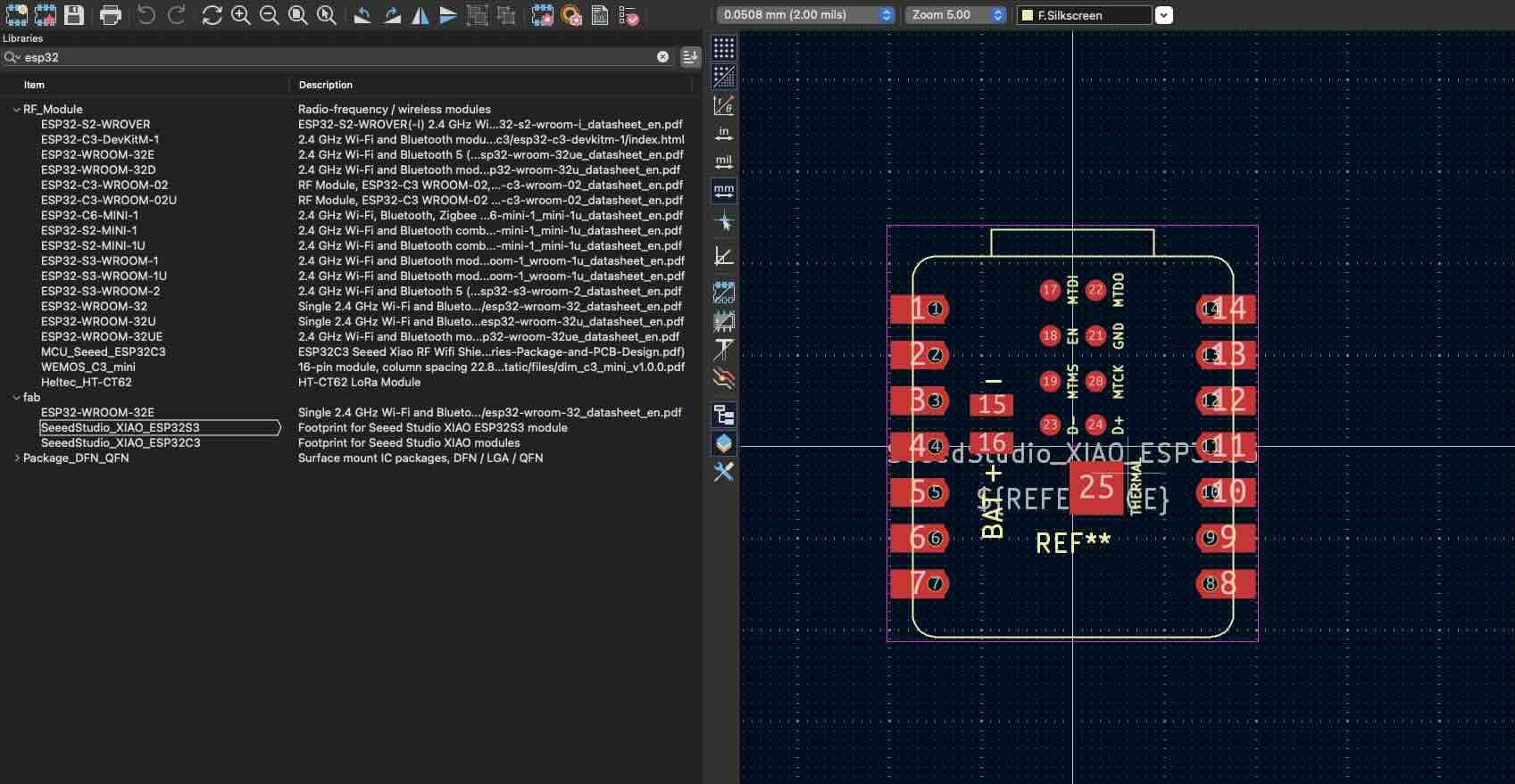
Currently, the most up-to-date library is available for KiCad, so I decided to use this software. Here you can find an introduction to Kicad. Kicad is a collection of tools for PCB development:
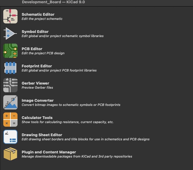
Mainly, you have tools for drawing the schematics of your system (Schematic Editor), the physical layout of your board (PCB Editor), and a symbol and footprint editor. The symbol and footprint editor allows you to modify the inputs and outputs of an electronic component, as well as adjust their physical dimensions.
To begin, you need to create a new project. It is important that all the elements of the board remain within the scope of the project. To create a new project:
File > New project
To import libraries: go to Preferences > Manage Symbols or Footprints,depending on what you need and then navigate to the symbol library or footprint directory that you want to add.
Below you can see some key buttons from the menu of the schematic tool.
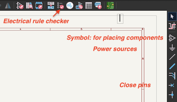
Some commands to manipulate symbols:
- G: Grabs and moves components while keeping their connections.
- M: Moves components, breaking connections — only the component is moved.
- R: Rotates components. You can combine it with M, for example.
- A: Adds a component.
In order to modify a symbol you can double click on it.
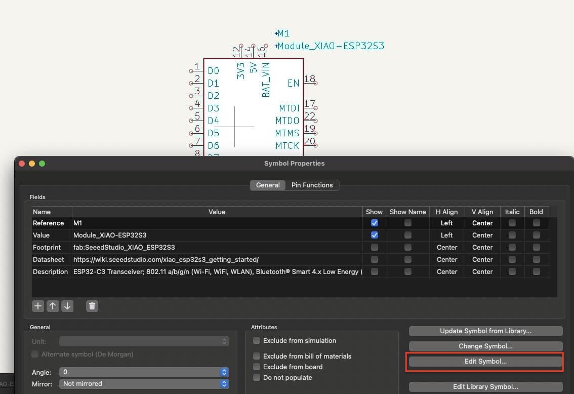
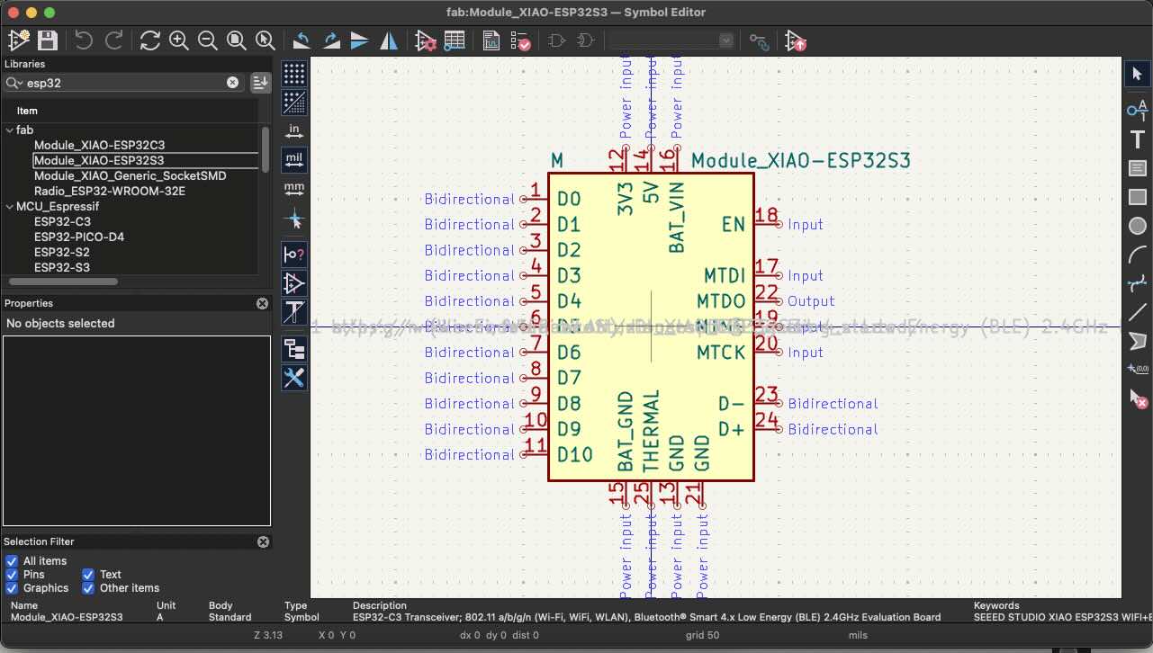
Symbols define the pins, such as power input, input, passive components, etc.
You also have footprints, which create a representation of the component’s real dimensions, allowing for its physical placement on the board.
Once we are happy with a design we go to the PCB editor to design the arrangement of the components and board shape and dimension.
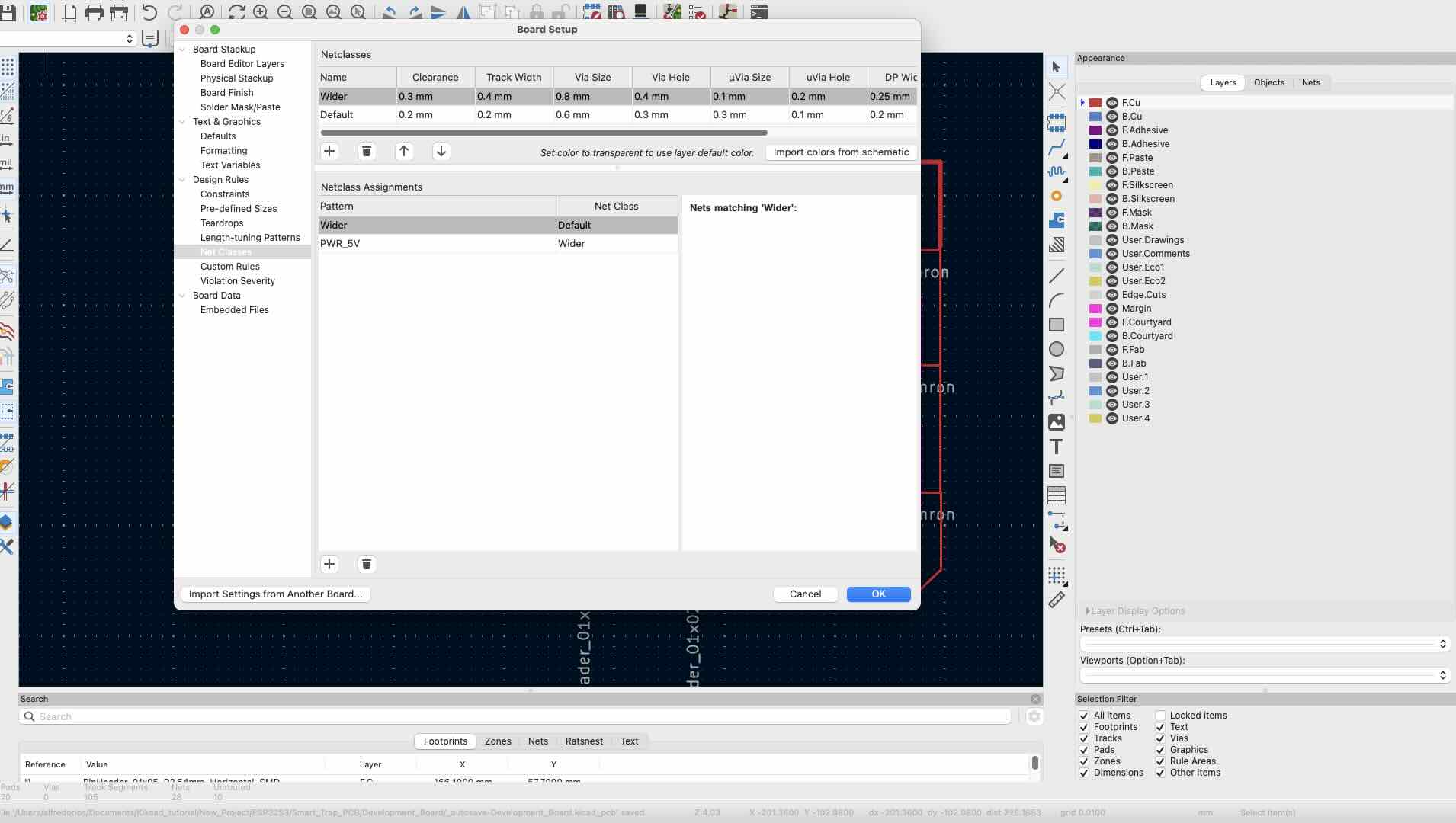
If you want to modify the design rules, you can do so in the board setup. You can use the constraints to set minimum values, and you can also define a net class for custom requirements.
If you’d like to modify a track in the editor, select the track, then press U to select all associated tracks. Afterward, press E to open the properties and change the width value. Ideally, it’s best to set constraints from the start.
One can set constraints
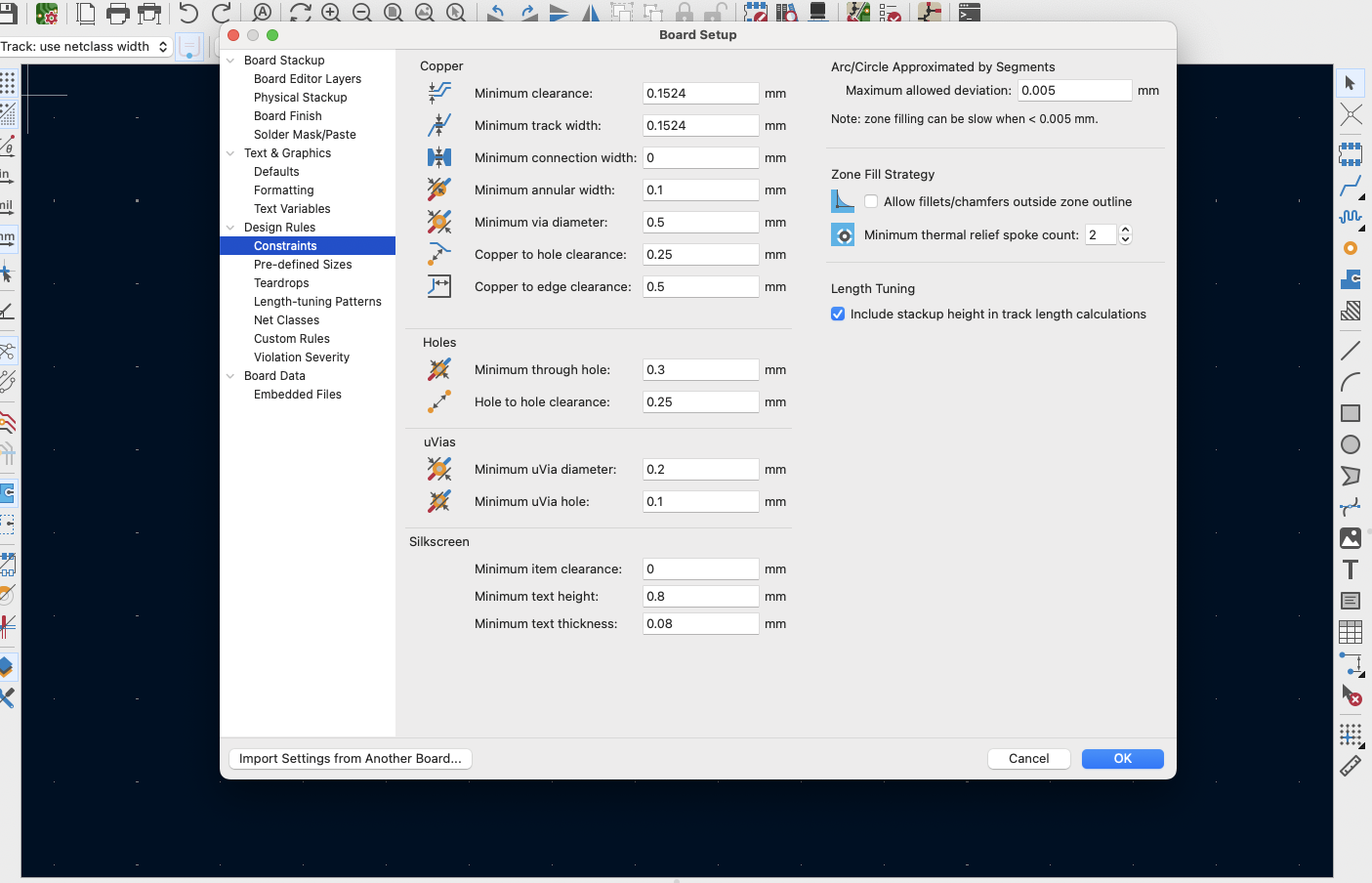
as well as classes
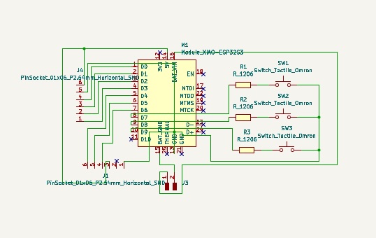
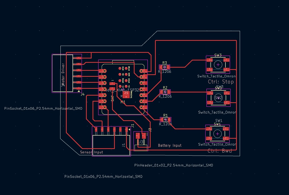
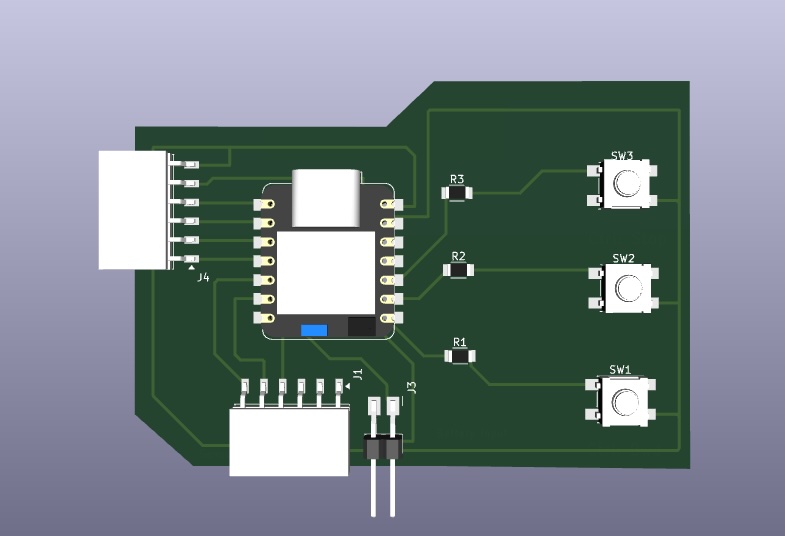
Finally, here is the board I designed (please see the note below).
Schematics:
Routings:
3D model of the board:
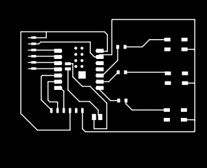
and a SVG file:
You can also find the BOM below,
| Component | Code | Units |
|---|---|---|
| Resistor | R1206 (1k Ohms) | 3 |
| Button | Omron B3SN | 3 |
| Pinsocket | Pinsocket 1x6 P2.54mm horizontal SMD | 2 |
| Pinheader | Pinheader 1x6 P2.54mm horizontal SMD | 1 |
Note: In week 8: I realized that there was a mistake in the board I designed above. This design is OK for a board with a micro controller that has pull up resistors, if that is the case the case the resistor I placed would have been redundant. I corrected the board design in week 8 by adding a pull down resistor to the buttons (link). I also had to reduce the number of buttons in the design.
Some thoughts about this week
- I was truly impressed with KiCad and the remarkable flexibility it offers for PCB design. The integration between the schematic and the PCB layout is particularly fascinating, as it streamlines the entire process.
- One feature that stood out to me is the 3D visualization tool. It’s incredibly useful for quickly identifying potential mistakes, such as components placed backward. Additionally, the ability to export an STL file to visualize how the PCB fits within the structural body of a device is a game changer when it comes to designing physical products.
- I also found that it is essential to set the production constraints from the outset. This approach saves significant time later by ensuring that all tracks and design elements meet the machine’s design rules right from the beginning, rather than having to tweak them one by one later on.
- I spent a substantial amount of time refining the schematic, mistaking that the schematic will also impact the physical layout while all of that is done in the PCV editor.
- Lastly, it’s critical to comply with the design rules and constraints set by the manufacturer. This attention to detail ensures that the design is not only functional but also manufacturable without costly revisions.
Here you can find a link to my project development page to see some additional info in regards to my final project (link )
Have you:
- Linked to the group assignment page
- Documented what you have learned in electronics design
- Checked your board can be fabricated
- Explained problems and how you fixed them.
- Included original design files (Eagle, KiCad, etc.)
- Included a ‘hero shot’