Electronics Design
This week, we smoothly started with electronic production. And I wanted to start working on something for my final project. You can find the plan for my final project here.
It is a wall element with a CO₂ sensor, featuring an RGB LED, sound output, and an LCD display. However, for an easier start, I want to create a PCB with a CO₂ sensor, an RGB LED, and a Bluetooth connection.
compontents for my first PCB
Xiao ESP32C6

CO2 Sensor MQ135

LED RGB DIFFUSED 6PLCC SMD

Some Resistor:
1. in 4,3Ohm

2. in 56Ohm

Choose programm for creating PCB boards
I had two options to create a PCB:
- KiCad
- Fusion Eagle
Since I am a Fusion fan and have spent most of my time using Fusion, I decided to use it. However, to learn more about it, I researched some good resources.
Eagle Fusion 360 from Autodesk (only testing)
![]()
1. Library of XiaoC3 from Seeed for Egale
Since I wanted to use the Xiao ESP32 C3 from Seeed, I needed the corresponding library:
Click here for the Fusion library of Xiao.
I downloaded the fab.lbr library and opened Eagle in Fusion 360 from Autodesk.
You can find it in the right drop-down menu:
Design > Electronics > New electronics library
Next, create a new schematic. At the top, you will find a Library menu. Click on the Library manager and import the new library
.
2. Use the schematics of Xiao
Click on Design. On the right side, you will see a menu with a list of libraries.
Search for Xiao, and you will find the correct schematic. Drag and drop the schematic into the workspace.
⚠️ Make sure to save your work, as Fusion does not have an automatic save feature.
Now, you need some additional components:
- LED light
- Resistor
At this time, many people have told me that it is better to use KiCAD as a beginner, and not many people can help me with EAGLE. So I changed my choice.
KiCAD (Open Source Programm)

1. Download and research KiCAD
And also make some research : Watch out the Youtube video to learn KiCad with a hello board click here for the youtube video And i watched a video about CO2 Sensor with Seeed Xiao ESP32 C6 click here for the youtube video for the first inspiration.
2. Download the library fab as a zip click here for the library
This is the fab library where you have some footprints maybe you need. For me it was important because the Xiao footprints are there.
On the Github site is a step by step explaning. Follow the construction.
Watch out the Youtube video to learn KiCad with a hello board click here for the youtube video And i watched a video about CO2 Sensor with Seeed Xiao ESP32 C6 click here for the youtube video for the first inspiration.
3. Footprint of sensors
Footprint library i used:
1. XiaoESP32C6
The XiaoESP32C6 is not in the fab library but the XiaoESP32C3 is there and I checked out the Pinout Diagramm and it is the same footprint. So I used the Footprint XiaoESPC3.

2. CO2 Sensor MQ135
That was a little bit complicated. I didn´t find the footprint of the Co2 Sensor. So it is a option to create a own footprint. But I didn´t know about it and for my finale I need a smd Co2 sensor. So for the frist board I change to the footprint for the Pin header. The Pin header is a basic footprint you can find at KiCad.
3. LED RGB DIFFUSED 6PLCC SMD
For the LED RGB I used Click here for the website How you import the footprint for KiCad use this Link
4. Schematics
1. Start with a new Schematic project.
And start with the board footprint. With the letter “A” you can open the footprint library or at the right menu.

2. Search the Xiao and open the ESP32C3. Palce the board in the middle.

3. Start with the Pin header for the MQ135. Click on the choose symbole button:

And search for PinHeader_01x04_P2.54mm_Vertical_THT_D1.4mm. This is the same distance from the MQ135.
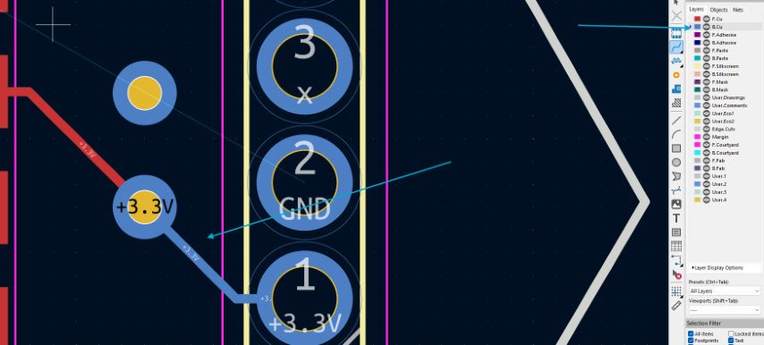
Connect the Analog Pinout (A0 for example) with the Pinheader. For these you need to create a line from A0 Board to the side and make a Label:


4. Now connect the Pin header with the xiao. First “3.3 Volt” Pin with the Pin of the header.

And at the Pinheader you need a Ground “GND”.

5. Also place the other components from the library LED RGB. Searching name: WL-SFTD_3535.
And than you can place the resitor for the LED. But for these you must look in the datasheet of the LED: datasheetLED and calculat it wirh a calculater: Calculater

Green and Blue LED have the same voltage. Red have a other voltage. So for this LED you need 2 different resistors:
Green and Blue need a 56 Ohm Resistor Red need a 4,3 Ohm Resistor
Now create the lines and label it with “BLUE GREEN RED”. ALso at the xiao Pinouts
D1 = RED
D2 = GREEN
D3 = BLUE


Place the restistor next to the LED RGB and with a right click go to the menu for the properties and change the value at the resistor to the 56 (you need two) and 4R3 (you need one). Create some lines between the RGBs and the resistors and place a GND next to every LED color.

6. So check out which pinout you didn´t need and mark them with a “x”

7. So bring the Schematic to PCB and save it before.

5. PCB
1. First, the individual components must be arranged on the board. It is important to ensure that no connections overlap. The components can be rotated and repositioned to achieve an optimal layout.
A useful method for better organization is aligning resistors in a row, which can be done by selecting the components, right-clicking, and choosing Align.


2. Once all components are well organized, vias need to be added to this design. First, I checked which vias were available in our lab. The suitable vias were THT 0.6. To insert them correctly, the following diameters were set under Properties:
Tube diameter: 0.6 mm + 0.1 mm = 0.7 mm
Annular ring diameter: 0.6 mm × 2 = 1.4 mm

Vias are used to move connections to the bottom side of the PCB. This was necessary in my design because the pin headers are soldered on the bottom side, requiring the connection to the traces to be routed downward.
3. Next, the traces must be connected to the components. Several important aspects must be considered:
The spacing between two edges must be sufficient.
There should be no 90° angles in the traces, as this could cause issues with the PCB milling machine.
Additionally, when placing vias, it is important to switch the layer to blue (bottom side of the PCB) to ensure the traces are routed on the correct side.
4. Finally, an outline as a Cutout is required.
I took the Outline as an dxf import from fuison to kiCAD:
Import a dxf to kiCAD click here

Place also the Ground area about the complete board. Click at the “Draw filled zone” and place it around the cutout with a little offset.

So now you can make a Simulation:

And make a Rule Check:

Warnings are not so important but you can fix them also in this case. But an Error need a controll. So I found out that the error of my PCB is not a problem. This is because KICad think the 3.3V Pinout is my power supply.
But in this case the xiao board have a mini USB port also (not showing in the footprint). But i fixed it with a power flag at the 3.3V at the board.
Now the first board is finish.
# Here are the files of this week:
Group assignment
As part of our group assignment, I learned the basics of electrical engineering. We also used an oscilloscope with a built-in LED indicator.
Check out the details of our group assignment here: Click here