08 - Electronic Production
General workflow to get from the KiCAD design to milling the PCB board is as follows:
kicad —> pdf __> png —> mods (Fabs module mills tool path generator)
Group Assignment
This weeks group assignment is documented here https://academany.fabcloud.io/fabacademy/2025/labs/barcelona/students/group-assignments/week8.html.
- Characterize the design rules for your in-house PCB production process: document feeds, speeds, plunge rate, depth of cut (traces and outline) and tooling.
- Document the workflow for sending a PCB to a board house
- Document your work to the group work page and reflect on your individual page what you learned
We documented the process of setting up the Roland SRM-20 milling machine to successfully mill electronic PCB boards, characterizing design rules and documenting the machine and tools settings. The milling process is very sensitive to mistakes made anywhere on the design and production chain, so collectively we have made a mountain of mistakes to learn from. Both the group and individual assignment pages provide solutions to a multitude or errors.
Individual Assignment
Kicad - design to print
There are lots of different layers in kicad. Only the F.Cu front copper layer and the outline are necessary for milling in the lab. The silkscreen shows the drawings and letters on the board which can be sent out for manufacturing. The fab layers are a silkscreen developed for the components in the fablab library.
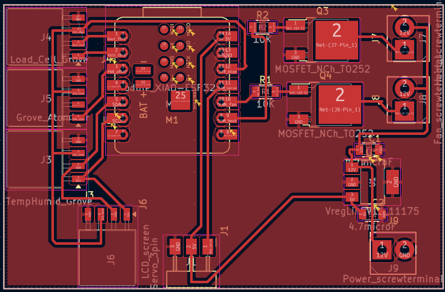
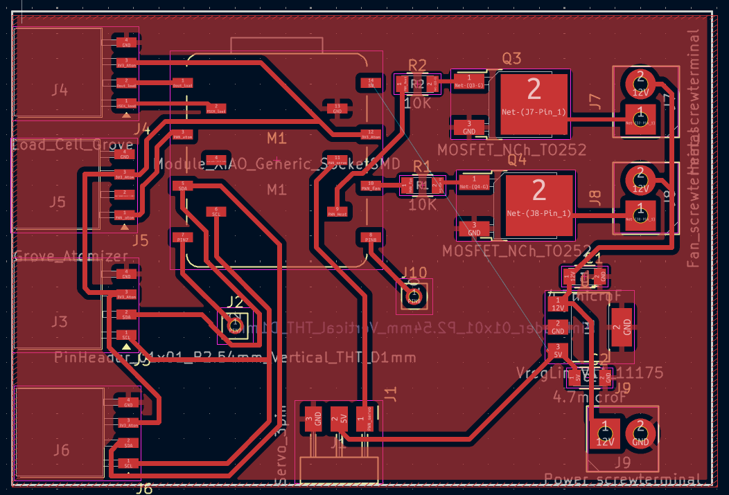
My KiCAD design was modified to better place the traces on the board and have a better access to the connections for the heat mat and the fan.
The F.Cu and edgecut layers were printed out as two seperate .pdf files to be loaded in inkscape.
The F.Cu and outline layers are selected and printed to pdf in black and white. Open the pdf in inkscape and create 4 layers :
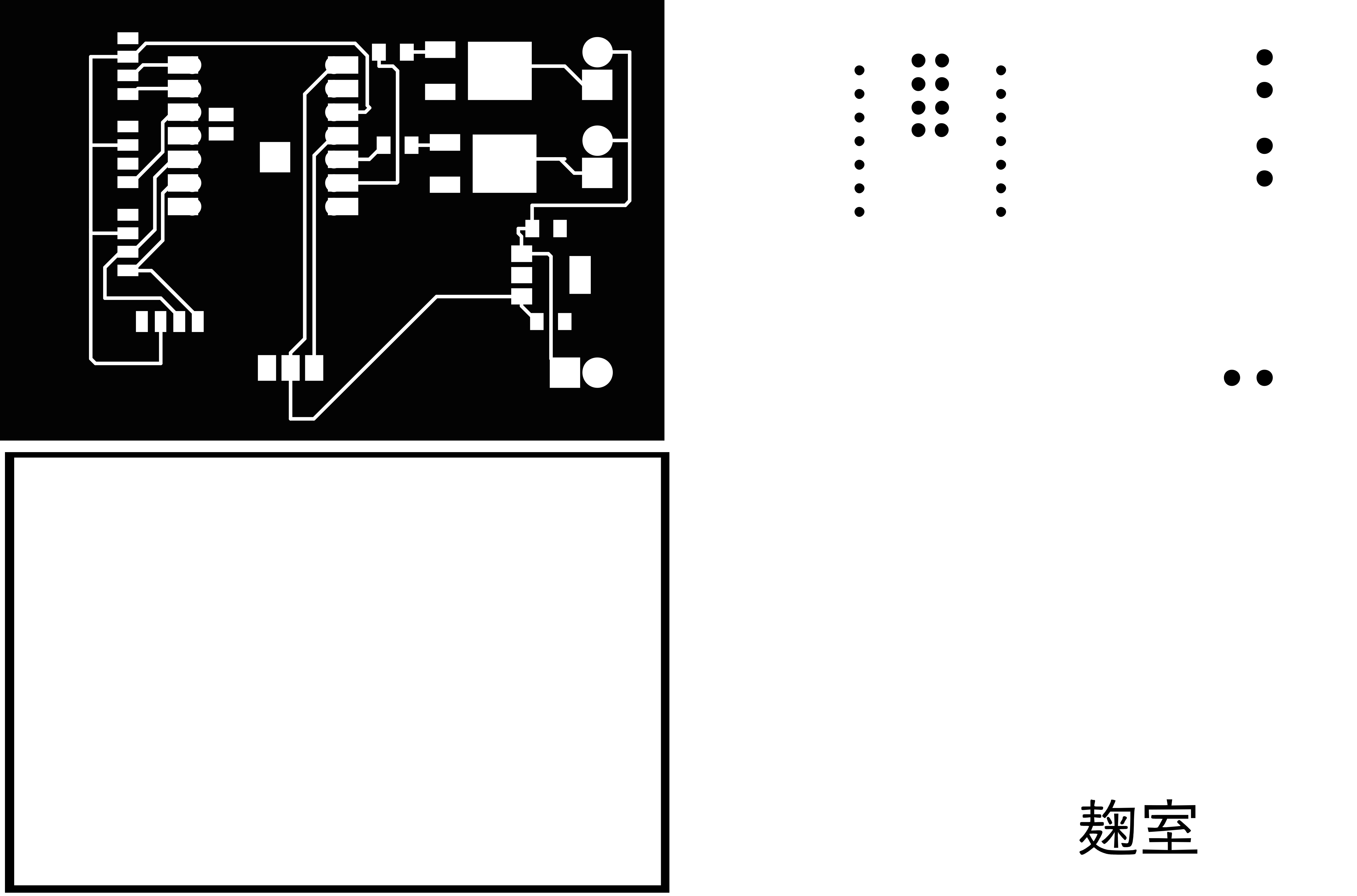
Select the holes and move to layer holes. A trick here is to click on one of the holes, Select Same - Fill and Stroke, to select all of the other similiar holes. Click on the eye to hide the holes to see what we have left to classify.
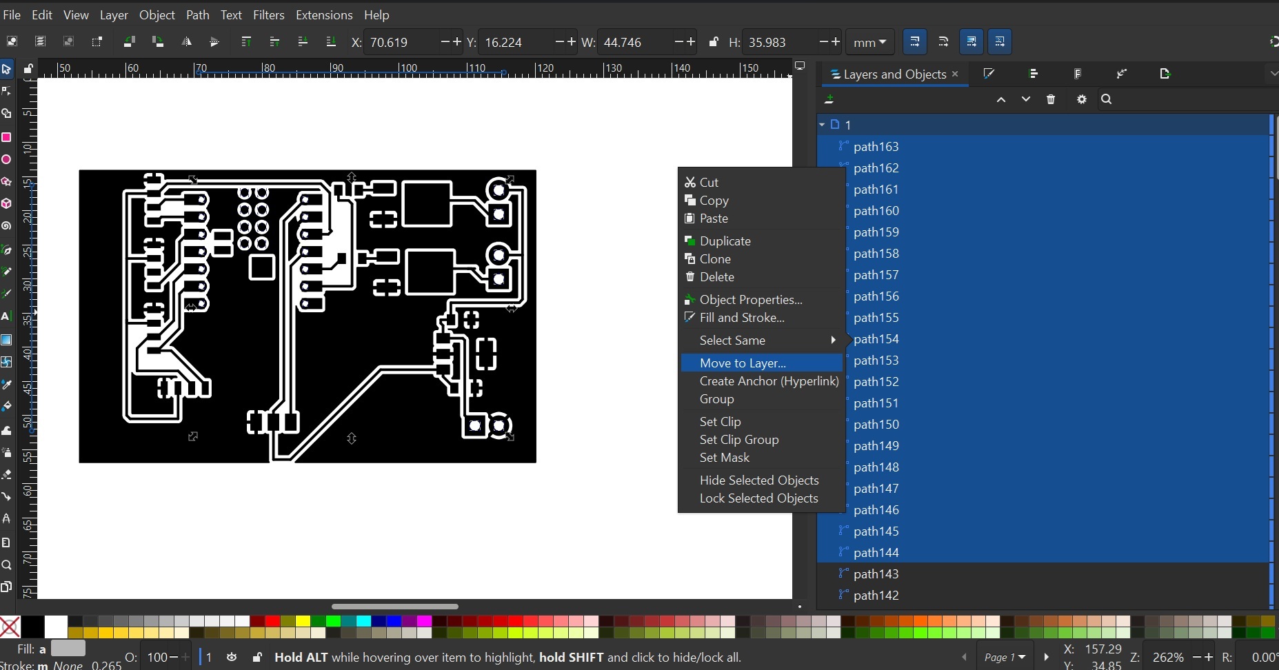
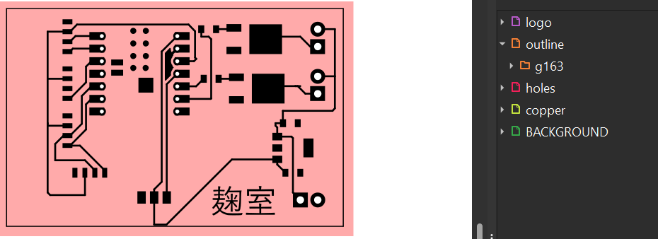
Repeat this step for the copper, outline and logo layers.
Next it is time to export the layers as png images. It is important to create a slightly larger background so that the outline png is exported correctly otherwise there is a risk that any traces closes to the edge are not milled correctly.
You can find the Inkscape file here:
Once all of the files are exported it is time to move to the modsproject software.
0.2mm limit to the thinnist size of line, the machine cannot assure a continuous line for thickness <0.2mm.
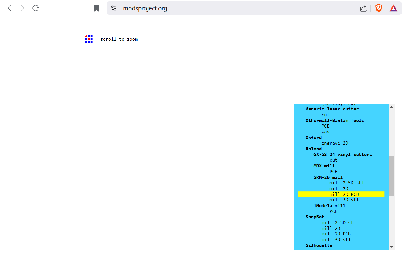
MODS project
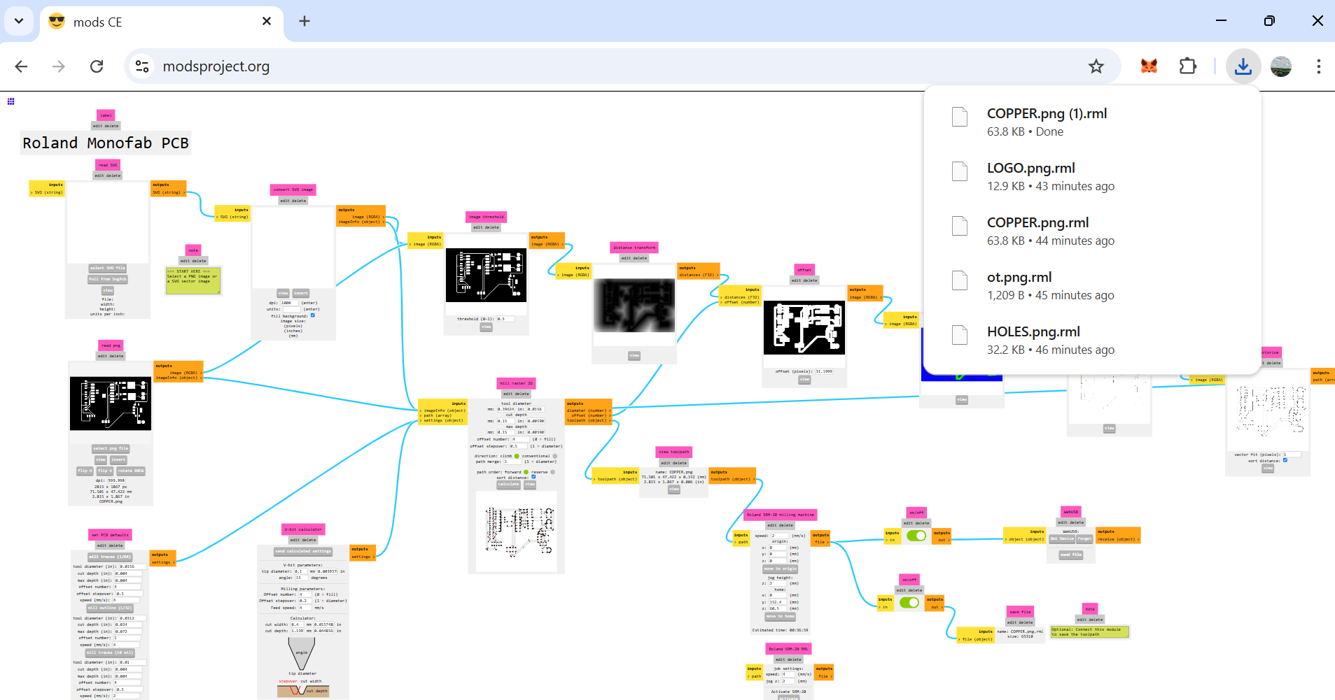
Save kicad design as png/svg to then add it to the modsproject.org tooling and machining program. Right click, programs and select our machine Roland SRM-20 mill. Use chrome or firefox as brave provides an errornous png file with extra dots.
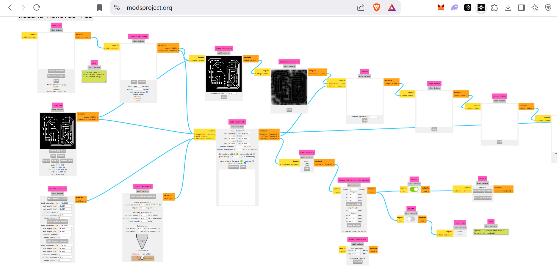
Select the 1/64 trace end mill and set the cut depth and max depth to 0.15 mm on mill raster 2D,
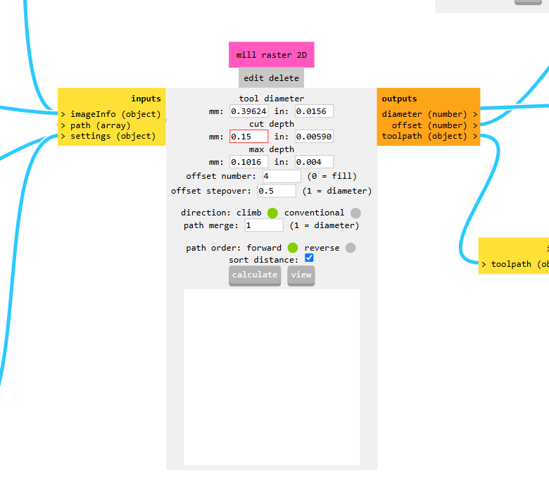
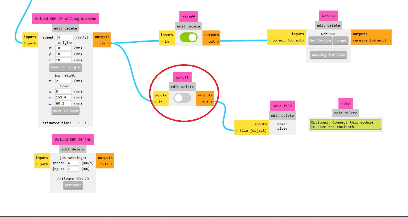
Set the machining speed to 2 m/s and the origin to [0,0,0]. Turn on the switch shown in the figure below and then click calculate to create the .rml file.
Next we have to create the tool path for milling the pin holes: select outline 1/32 end mill, verify the cut depth that it is 1/3 of the max depth (it will take 3 passes) and change the speed of milling speed on the machine to 2 and set the xyz origin to [0,0,0].
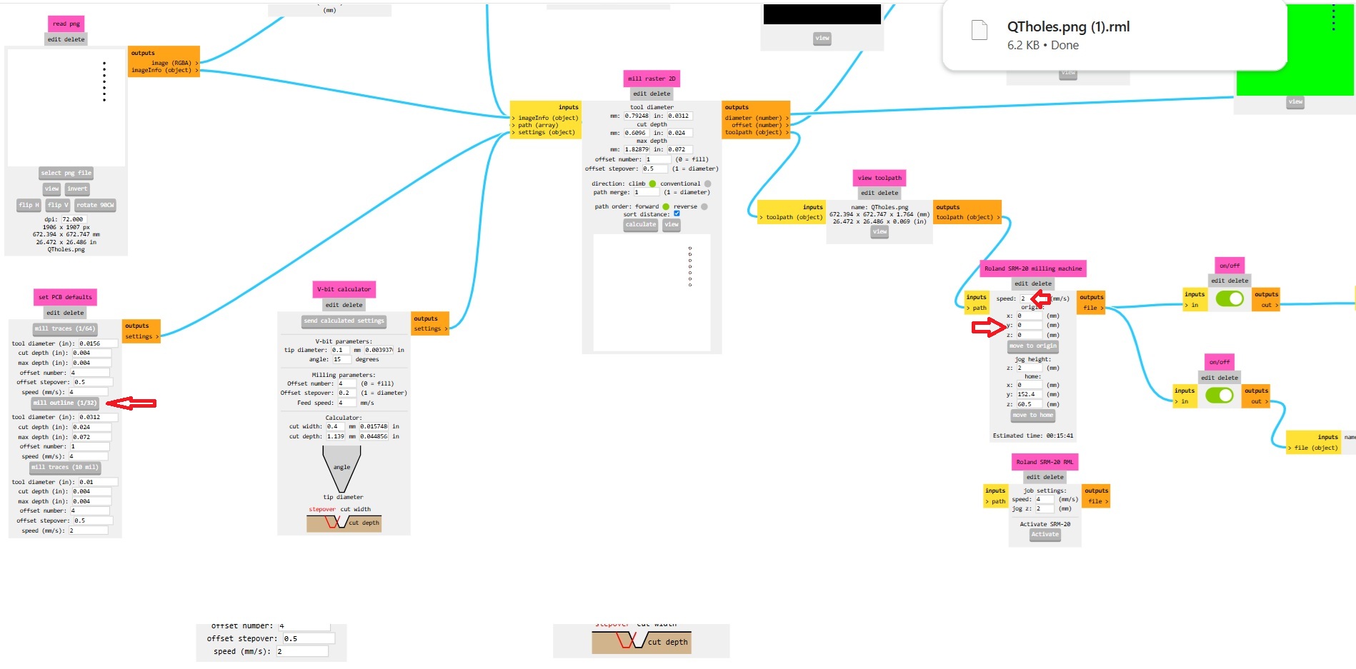
The final design step is to create the tool path for the outline of the board, using the same setting as the 1/32, as the end mill is cutting the final shape of the board. This is a separate file to the holes as the sequence of cuts can’t be defined in the machine.
The results of this process is .rml files that will be used by the Roland mill to mill the board.
.rml)
Milling on the Roland mill
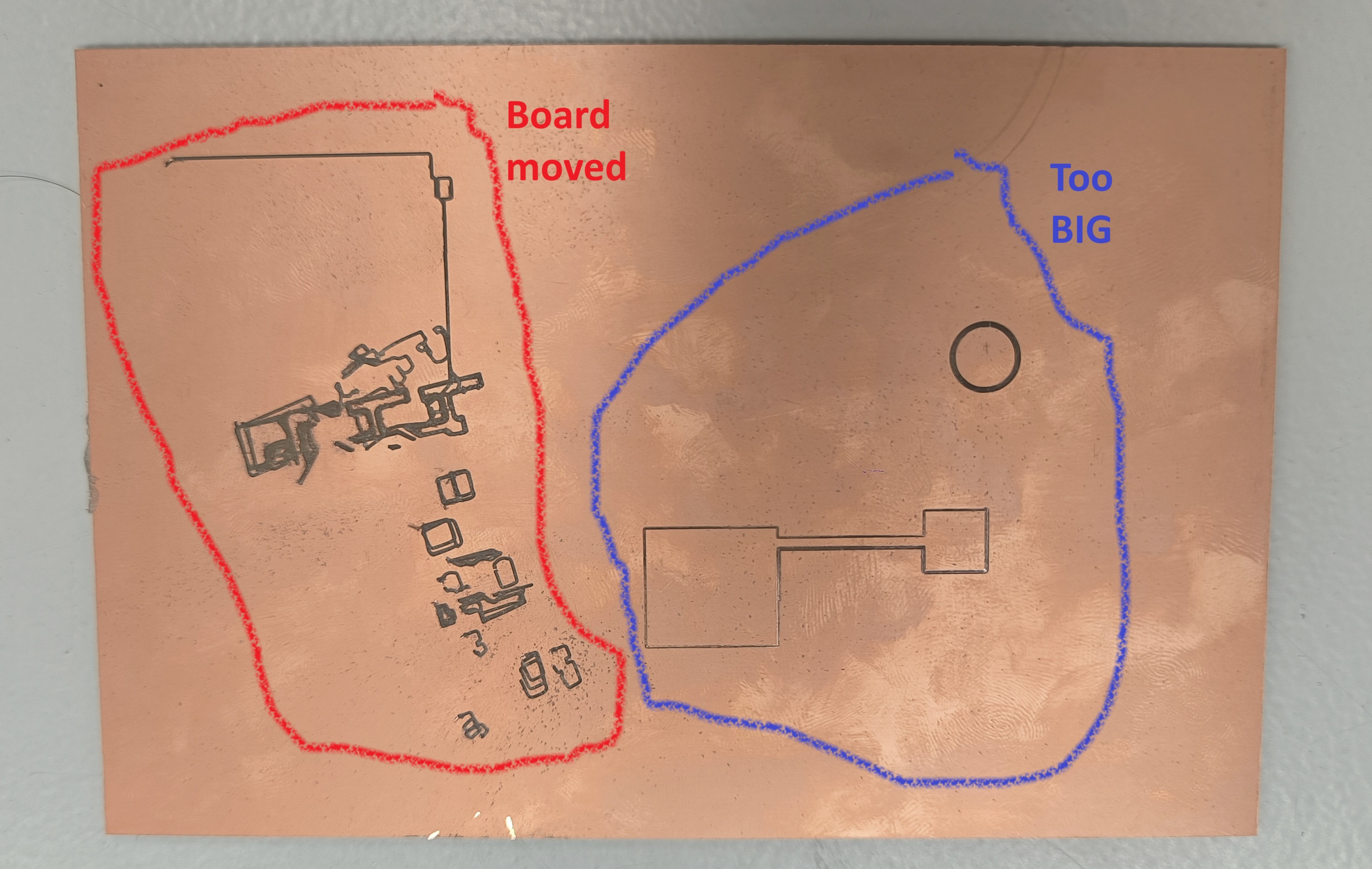
The first thing to do add double sided tape to the back of the board we are cutting. Ensure that there is enough tape used and that it is securly fastened otherwise it may move and you will end up with a trashy board like we can see in Figure M1 below.
It is also important to print the pdf file from Kicad at a 1:1 scale, as if you select fit to page you may end up with everything being too large like you can see the huge spacing made for a mosfet in Figure M1.
Completed Board
After a few iterations I finally got to mill the board correctly. It looks lovely and it works !
Here is the latest PCB layout, after moving the grove connectors slightly to have enough space to fit them on the board!
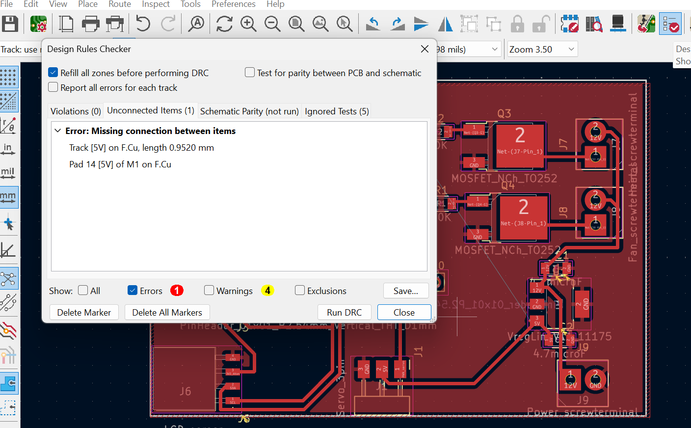
It’s important to use the design rules checker to make sure there are no serious problems with the design before milling, I made a couple of boards where their were ground islands not connected to the same ground as the microcontroller.
The final board can be seen below: glue was used on the grove connector to give extra strength, as they pulled off the board on previous versions when connecting and un-connecting devices. Although the grove connectors are handy, they don’t appear to be appropriate for frequent changing of components.
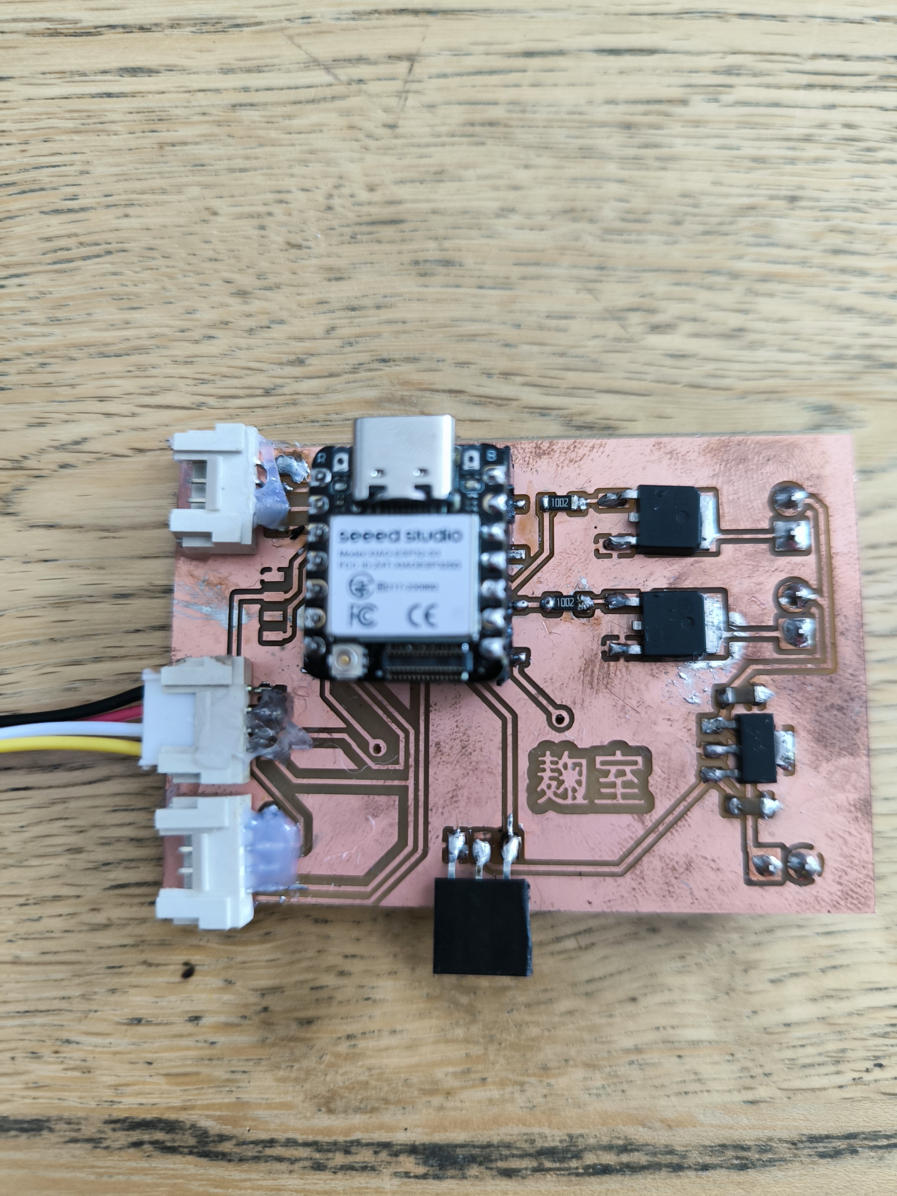
Overall I am now happy with this board.
KiCad:
Inkscape :
PNG files for mods:
.rml files for milling:
I checked that the lines are connected with the multimeter and verified that all of the grounds were correctly connected without any unwanted issues.
The board has been tested in weeks 9 and 10 and works well for both outputs and inputs. You can see the source code and videos of it working in these weeks.