06 - Electronics Week
Group assignment:
Objective:
- Use the test equipment in your lab to observe the operation of a microcontroller circuit board (as a minimum, you should demonstrate the use of a multimeter and oscilloscope)
- Document your work on the group work page and reflect what you learned on your individual page
More details about our assignment can be found here https://academany.fabcloud.io/fabacademy/2025/labs/barcelona/students/group-assignments/week6.html
We played around with the Oscilloscope and multimeter so we have been introduced to the key versatile tools required to diagnose and trouble shoot circuit and electrical issues.
Individual assignment:
- Use an EDA tool to design a development board that uses parts from the inventory to interact and communicate with an embedded microcontroller
KiCAD setup
Once KiCAD is successfully installed on your computer it is time to install the libraries:
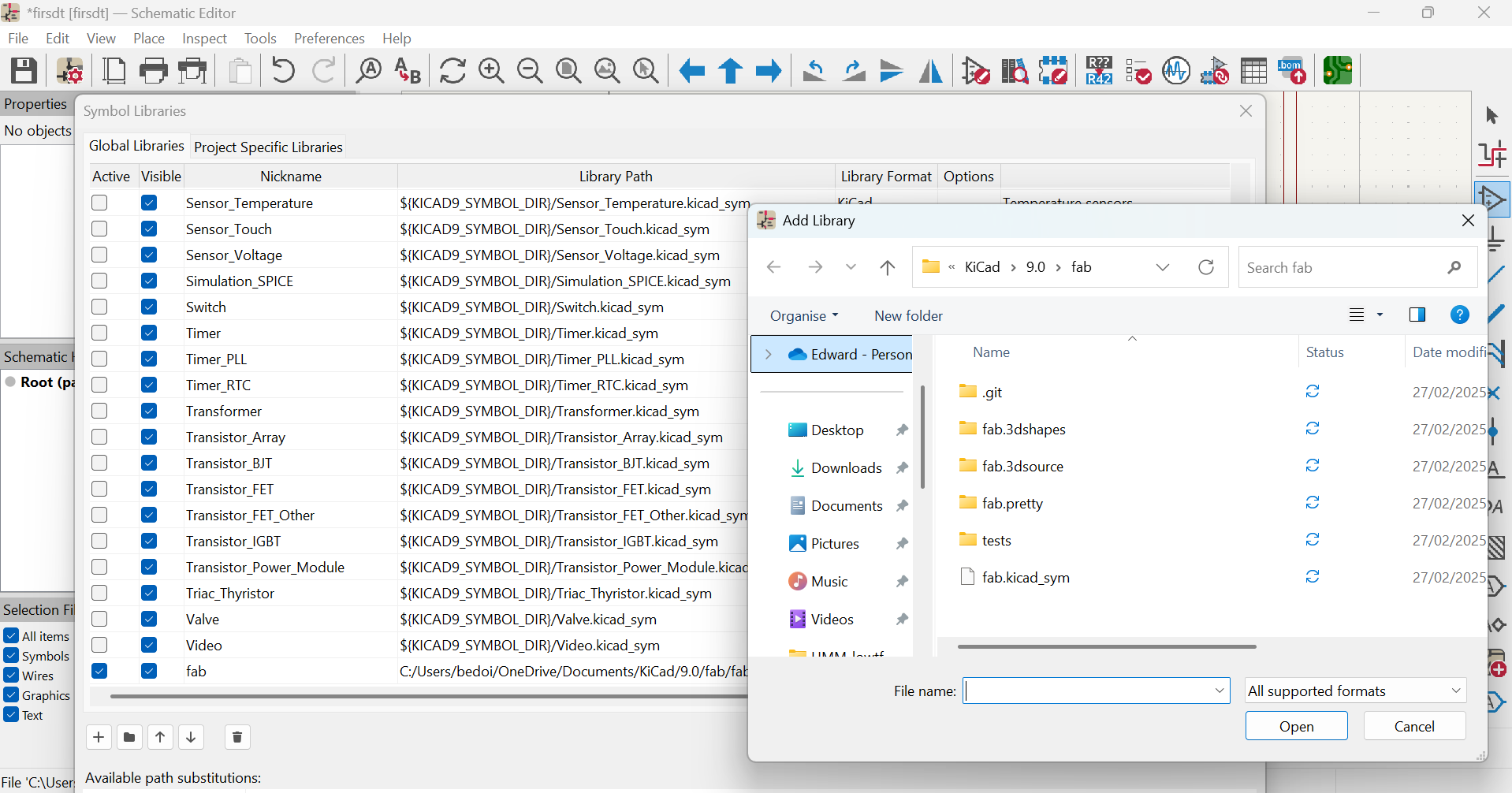
Open Preferences/Symbol Libraries and deactivate all of the current symbol libraries then add the file fab.kicad.sym
Next it is time to set up the board :
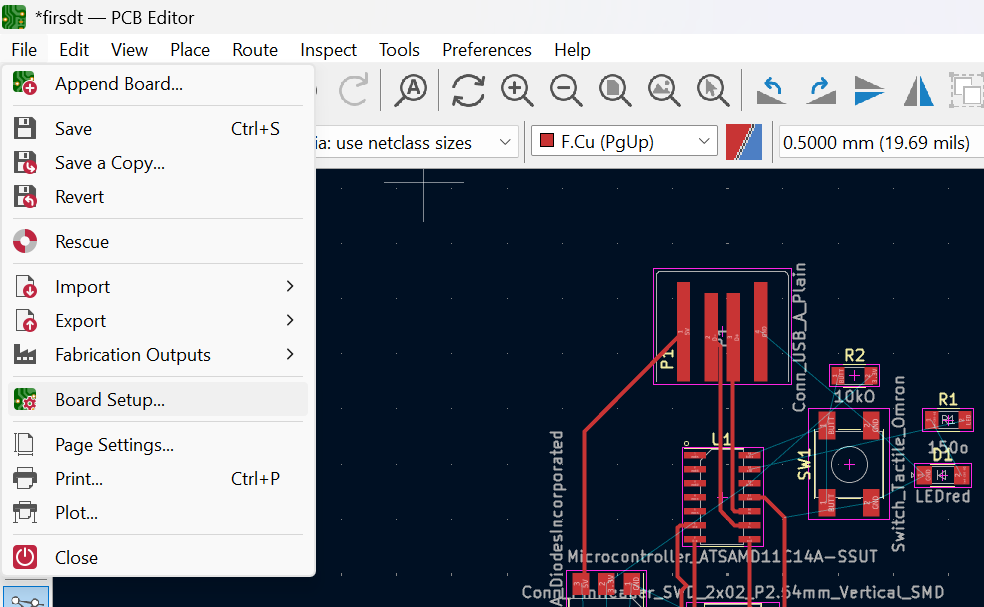
Open File/board setup/net classes and enter the following settings:

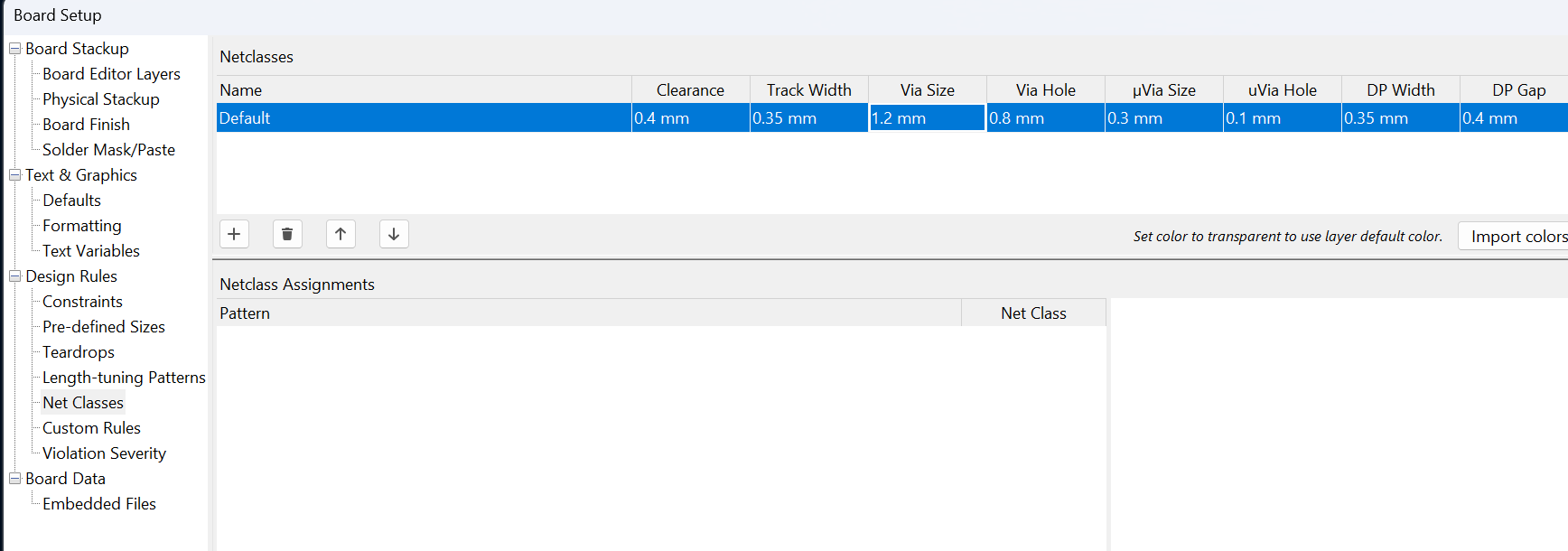
- Clearance 0.4 mm /callout
- Track width 0.35 mm - for hand craft
- Via size 1.2 mm - copper around hole
- Via hole 0.8 mm - hole
- DP width and gap = differential pair 0.35/0.4
Koji Fermentation Chambers’ Board Design
Now it is time to design a board. I’m going to design a protype board for a Koji Fermentation Chambre. I first wrote a little pseudo code for what is required in the system:
read Temperature and Humidity of the chamber
read weight of the substrate

heat up substrate/chamber
cool down substrate/chamber

increase humidity in chamber
decrease humidity in chamber
The inputs of the system are therefore Temperature, Humidity and Weight measurements. The outputs of the system are heating, cooling, misting and ventilation.
Choice of components
Key considerations I would like to incorporate into my design are the following:
1. Use MicroPython or TinyML for possible feedback  --> Xiao RP2040
2. User Interface --> LED / OLED screen + buttons
3. Interchangable/Modular/Spiral Design --> SeeedStudio / Removable Connectors
I looked in our Fablab and in the SeeedStudio repository for potential inputs and outputs.
Input devices:
- Function: T/H sensor
Component: https://www.seeedstudio.com/Grove-Temp-Humi-Sensor-SHT40-p-5384.html
- Function: Scales and dynamic weight readings
Component: https://wiki.seeedstudio.com/grove_adc_for_load_cell_hx711/
Output devices:
- Function : Ventilation
Component: Fan : ADDA 12V, 0.3 A
- Function: open and close A/C flaps on the wall of the chambre for better circulation/ventilation.
Components: Cooling flaps open with a rudder controlled by a servo moto, 180 degrees:
- Function : Misting
Component: https://www.seeedstudio.com/Grove-Water-Atomization-v1-0.html
- Function: Ultrasound emittor
Component: https://wiki.seeedstudio.com/Grove-Ultrasonic_Ranger/
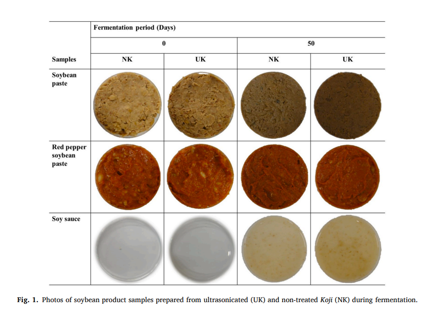
2022 Paper shows that ultasonicated Koji at 30kHz can improve amino acid production leading to a more flavourful and darker soy sauce.
https://www.sciencedirect.com/science/article/pii/S0023643822008714


The majority of the components above are Grove connected modules from SeeedStudio. These modules fit into my third design principle hoping to integrate modularity into the design allowing for a continuous spiral design.
Connectors
Typically connectors have a pin spacing of 2.54mm whereas Grove connectors have a pin spacing of 2.0 mm.
Use Grove connectors for an easy to operate system
https://wiki.seeedstudio.com/Grove_System/
4 types of rove connectors, generally they are the same : signal 1, signal 2, power and ground. It is a modular standardized connecter prototyping system. The connectors are made so that they only connect correctly and are designed such that if you plug in the wrong type of base unit there is no problem, it just won’t work. With the exception of plugging a 3.3V I2C module into a 5V i2C connector could fry the device.
Grove Digital
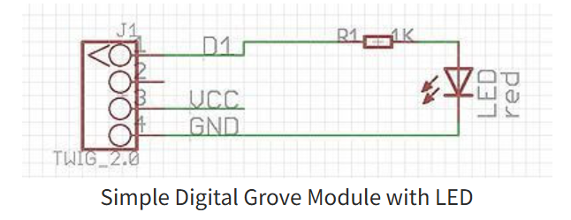
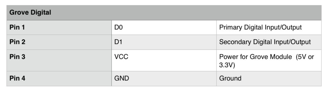
examples of grove digital modules are : switch modules, fan modules, LED module.
Grove analog
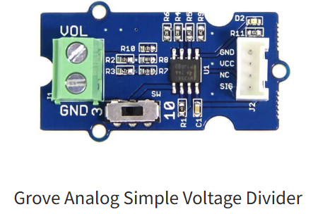
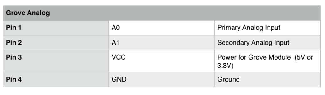
Four standard lines coming into the Grove plug: two signal A0 and A1, VCC and GND. Typical examples : Potentiometer, Voltage Divider and Grove Air Quality Sensor
Grove UART
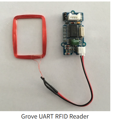
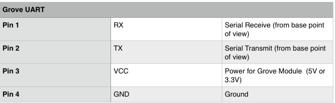
Specialised Grove Digital Module. Pin1 and Pin2 for serial input and transmit. Pin 1 is RX (base unit uses to recieve data, input) Pin 2 is the TX line (transmit data to the Grove module).
Examples : XBee Wirleless Sockets, 125 KHz RFID reader
Grove I2C
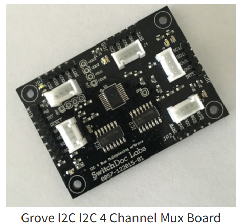
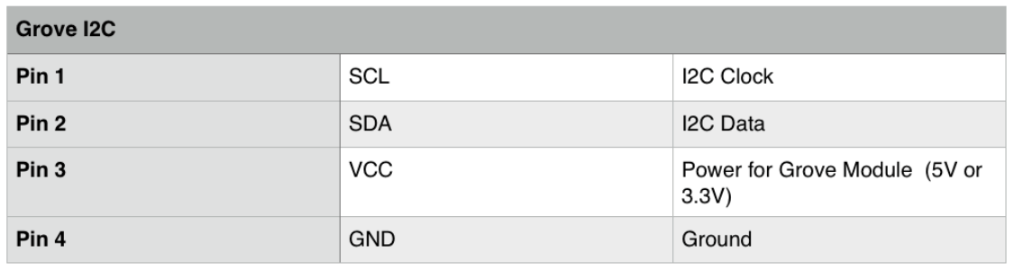
Some devices only come in 3.3V or 5V. Pin 1 SCL signal, Pin 2 SDA Signal then Power and Ground.
open the Schematic Editor and start to add the components. The shortcut for adding components is “a” for add.
KiCAD design
The “Go-To” for electronic board design at the fabacademy is https://gitlab.fabcloud.org/pub/programmers/quentorres
I’ve separated my project into different functions:
- Power and Voltage regulation
- Microcontroller
- Input Devices
- Grove output devices
- 5V output devices
- 12V output devices
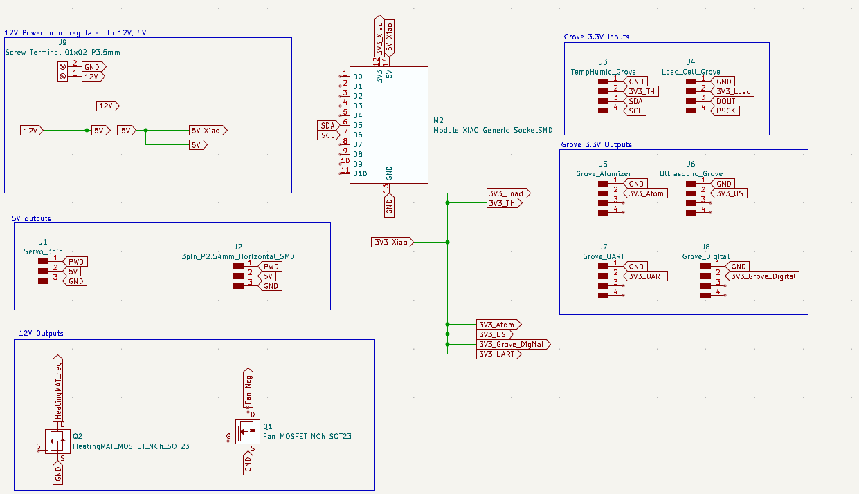
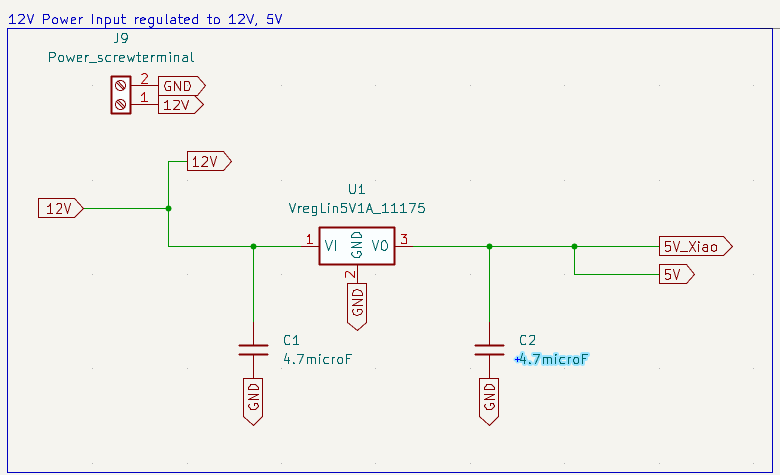
Powering the circuit
From here I have to look a how I can successfully separate the 12V supply into multiple two lines for the 12V (to power the heating mat and the fan) and 5V (to power the servo, the Xiao and it’s downstream inputs and outputs).
Chapter 11N of “Learning the Art of Electronics A Hands-On Lab Course” by Tom Hayes & Paul Horowitz [1] is dedicated to voltage regulators. Voltage regulators strive to provide a constant voltage output despite fluctuations on both input and output current loading.
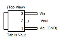
At the FabLab BCN we have LM2940 IMP-5.0V voltage regulators in stock. In order to understand how this is used in the circuit we go to the datasheet which can be found here. Page 8 in this datasheet gives the design requirements and the Typical Application:
It’s important to check the operating conditions and the pin layout, as the layout can change significantly from one manufacturer to the other, as I found out when I fried a Vregulator testing it with the oscillator.
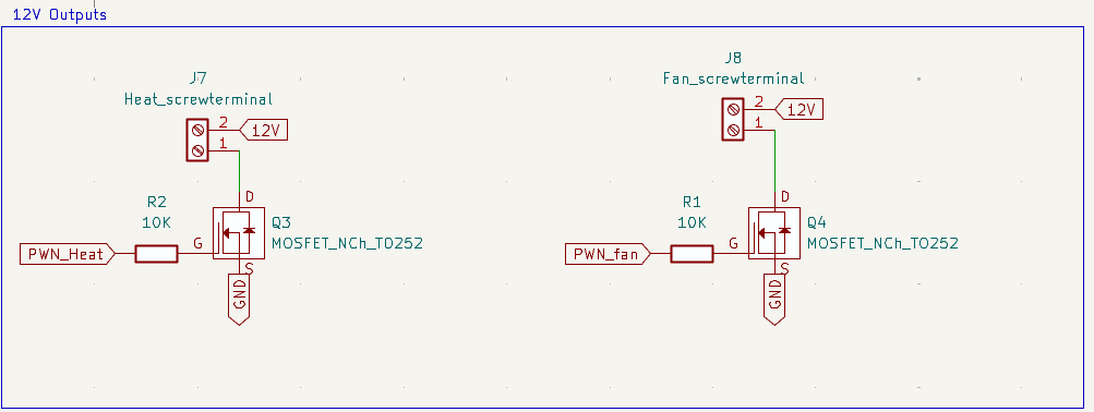
Powering the 12V outputs
The heating mat and the ventilator require 12V input. The heating mat is the most energy heavy and is to be sized at a later time when I have determined the size of the koji fermentation chambers. The ventilator requires a 0.3A current.
In my design I am going to use an n-channel MOSFET as a true on-off switch powered by the micro-controller. The most suitable MOSFET available currently at our lab is this one. The other common N-Channel (negative channel in contrast to positive channel, which is constantly on until
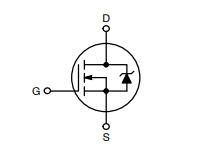
The drain D comes from the load, the gate G is powered by the microcontroller and the source S goes to the ground.
Looking at our design, the Gate voltage comes from the MCU, the positive from the 12V power supply is connected to the load via a screw terminal, the negative then feeds back through the screw terminal and feeds into the drain of the MOSFET. When the voltage is output from the MCU the power is switched connecting the drain with the grounded source. This is shown in figure KC6 below.
Choice of MCU
A review of the principal input devices allows us to determine the most appropriate MCU for the job in terms of the number of analogue pins that are solicited.
Inputs:
- T/H sensor - SDA/SCL
- Load cell - Analog PSCK input / Digital output
Outputs:
- LCD screen - SDA/SCL
- Atomiser - PWN analogue input
- Servo - PWN analogue input
- Heat mat - PWN analogue input
- Fan - PWN analogue input
A total 5 analogue pins, 2 SDA and SCL pins and a digital input pin is required to reach the objectives of the board.
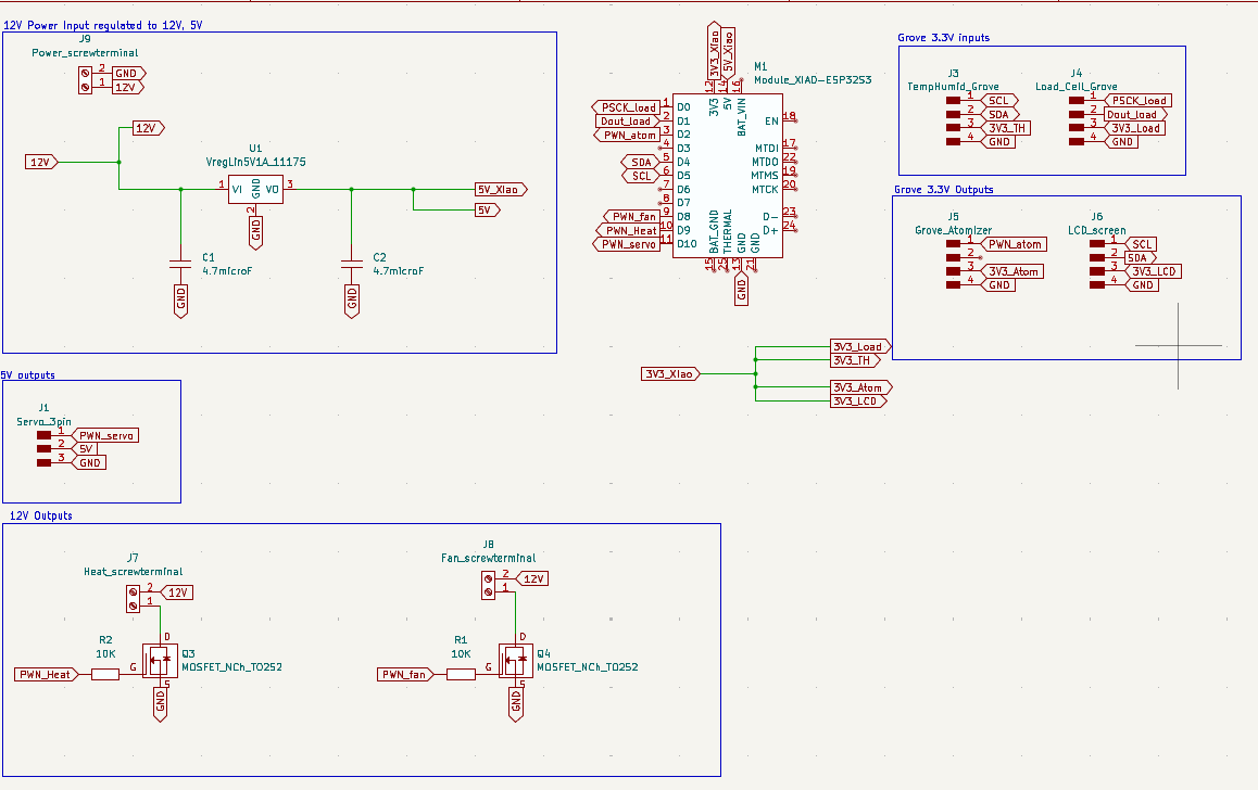
You will notice several changes in the design compared to Figure KC1, this is to accommodate the number of analogue inputs and also to optimise the PCB design.
PCB Design
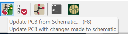
Now that the we have a KiCAD design that I am happy with it is time to move on to the PCB board. We open up the PCD design editor and update the PCB design with the KiCAD components from the Schematic Editor by clicking F8 or the following button:
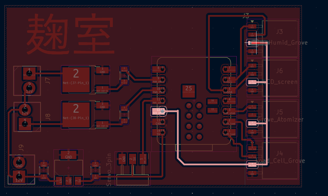
It’s time to arrange the different components in a manner in which will allow the traces to be neatly connected to the various components ensuring that there isn’t an open loop. This took several iterations, and I decided to use the board itself as the common ground to simplify the traces using the Draw Rule Areas
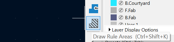
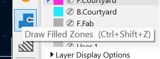
Figure PCB2a: Draw Filled Zone
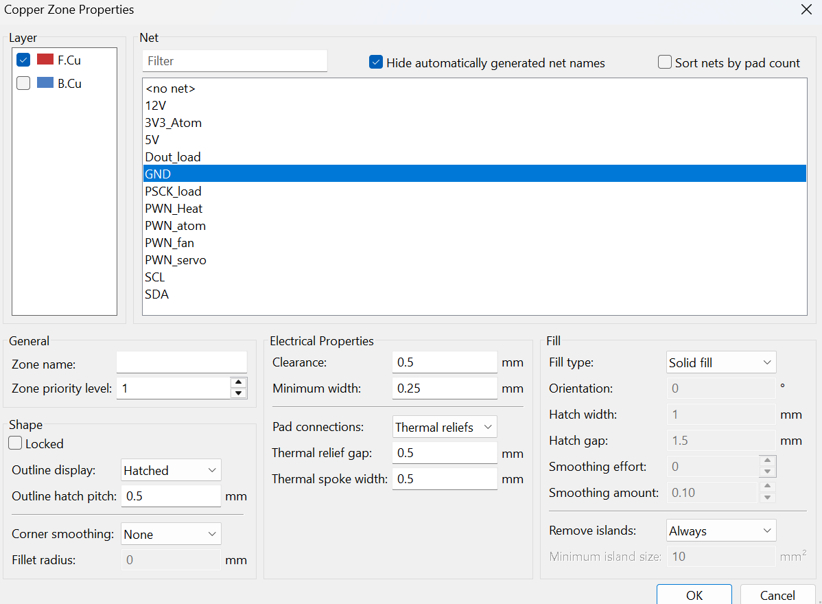
Once the fill zone has been drawn and the copper zone area has been set to GND, it is time to start tracing the paths between components.
The minimum clearance 0.45 mm and track width 0.4 mm of the traces are defined in the Board Setup/Constraints:
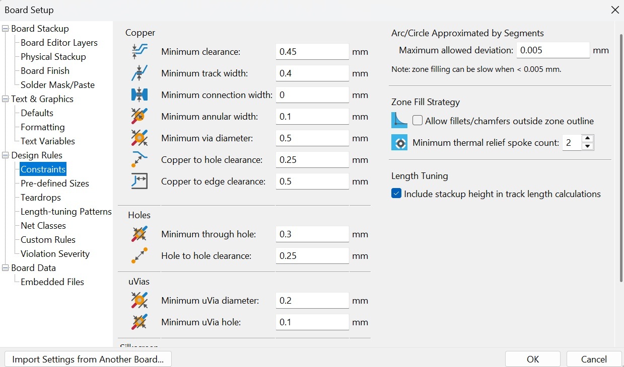
As a general rule, the paths with higher currents running through them should be wider to reduce unwanted thermal heating.
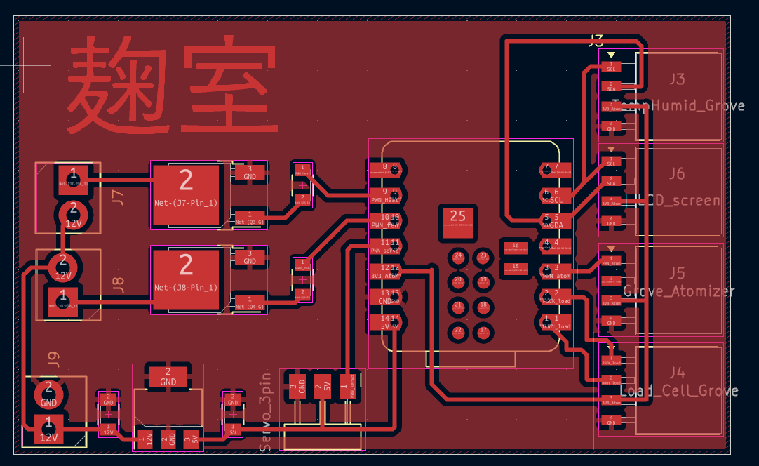
The traces were then eloquently drawn between the relative components, the labels from the schematic made it easier to know which components are to be connected with each other, for example you can see the all of the components requiring the 3V3 line in the figure PCB4 below.
Once I successfully connected all of the componest together I decided to add the Japanese symbol for Koji-Muro to the board, uploading it as an FVG. Here is the finalised v2 PCB board that will be printed out in week 8.
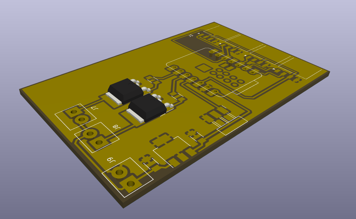
The board has since been updated for better use as a development board, the KiCad files for version 7 are given below.
References
Learning the Art of Electronics A Hands-On Lab Course” by Tom Hayes & Paul Horowitz https://artofelectronics.net/ [1]