08—Electronics Production
Assignment
- Group assignment:
- Characterize the design rules for your in-house PCB production process: document feeds, speeds, plunge rate, depth of cut (traces and outline) and tooling.
- Document the workflow for sending a PCB to a boardhouse
- Document your work to the group work page and reflect on your individual page what you learned
- Individual assignment:
- Make and test a microcontroller development board that you designed
00—Reflection
PCB making was a bit of a struggle. Mostly because I was rushing through the process a bit too much. I would rather work quickly though with something like this because it lets me go through the whole workflow more than once. That said I could have just been a bit more careful during soldering the first PCB… Early in the week I was mostly trying to work out my final project concept. I have a solid idea of what I want to do, but I needed to figure out how the composition should work. I also needed to check in with myself if it was an art piece worth making. So I was mainly concerned with the question “is this worth my time?” “will this be visually impactful?”.
Basically, at the moment I am working through the disenchantment phase of my project. The initial excitement has warn off and I need to address some of the fundamental questions of the project. These are the technical and aesthetic problems that I was aware of in the beginning that seemed trivial, but this weekend I realized some of them might actually threaten the intent and goals behind the final work.
01— Group Assignment
For the group assignment we did a custom PCB to send out to a PCB manufacturer.
02— Basics of PCB Milling
Notes From Class
- We are milling FR1 copper resin substrate so its got 1 layer of copper and 1 layer of FR1. This is what you use for milling. It is not a good heatsink so it can’t be used with hot plate based soldering process.
- A vinyl cutting process can be used for creating flexible PCBs. Hong Hao Deng documentation on how to create vinyl cut PCB https://fab.cba.mit.edu/classes/863.17/Harvard/people/HonghaoDeng/project-3/project-3.html
- Zeroing the tool properly is very important make sure you don’t over tighten the bit this will lead to inaccuracy.
- have just an ever so slightly used endmill will give you the best edge finish
- 50mil pad spacing is a distance that can be repeatedly achieved with a common endmill size like 1/64”
03— Full Workflow PDF to PCB
Process Overview
- Output Files: The board we are creating uses surface mount components which means there are no through hole components. What we need is a black and white PNG with 1 layer per machine operation. That is generated in KiCad → processed in Adobe illustrator → processed individually in separate Mods projects
- Machining Operations: In my case I have traces (1/64” endmill), mounting holes (1/32” endmill), and the outer profile (1/32” endmill). Mounting holes and the outer profile are separated so that mounting holes operation is ran before the outer profile because the machine software has no ability to order the program. In this case mounting hole need to be before the outer profile because they are inside cuts.
- The Machining: As mentioned before we are using 1/64” endmill and 1/32” endmill. Basically the bare copper FR1 board needs to be securely mounted with tape the machine needs to be zeroed and then the three programs are ran.
Prepping in KiCAD
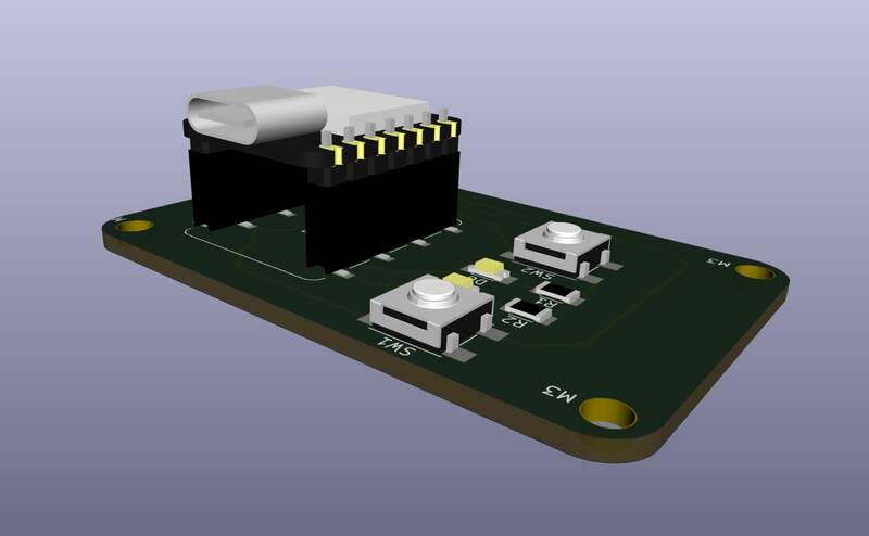
- The first step in the process is KiCAD. Here it is assumed that a finished board that is designed within the capabilities of the machine has been designed beforehand.
- Go to footprint workspace of finished board
- Click
printand export the relevant layers. In this case checkF.Cu(our top layer traces) andEdge.Cuts(our PCB profile).
- Save as PDF within the print dialog
- Open illustrator click top bar
file → openselect the PDF you generated. The file needs to be imported this way versus dragged in to allow for proper editing.
- Now this is a bit more of an art form, but you essentially need to make sure objects are properly demarcated. Delete the white background and use a combination of the
uniteanddividepathfinder functions.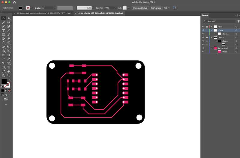
- Now you need to group your elements in separate layers. The layers you need are your trace, holes, and edge cuts. There are different way to go about isolating and grouping them, but you should be able to figure out how to do this if you know the basics of Illustrator ;) .
- Final output: This should be your resulting output exported in PNG at 1000 DPI.
Loading The PNGs Into Mods
- This process will need to be repeated for every machining operation. The slight difference in settings for the various controls is noted below.
- Open Mods website (works better in Safari and Firefox in my experience)
RMC → programs → open program → SR-20… Mill 2D PCB
- Bring your Traces PNG into the
Read PNG block
LMC → traces preseton Set PCB Defaults- For the holes and profile layers choose
LMC → mill outline preset
- For the holes and profile layers choose
Cut DepthandMax Depthset to .15mm on the Mill Raster 2D block
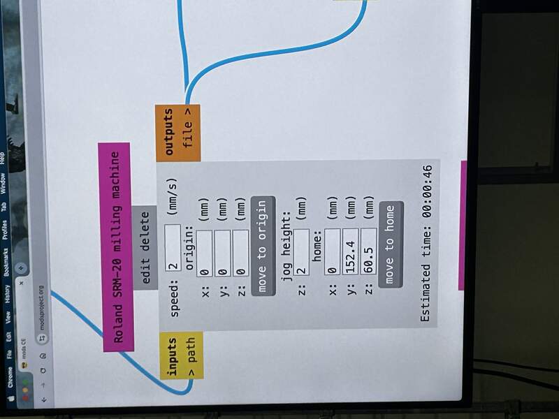
- On the Roland SRM Milling Machine… block edit the following:
Passes[2] X[0] Y[0] Z[0]
- For the input output Roland SRM Milling Machine… there is a slider button in the off state as default, change to
On/Off [ON]
- This automatically downloads the machining file to your computer.
- Rename the files and place in a folder to be brought over to the Mill!
Machining With The Roland SRM20
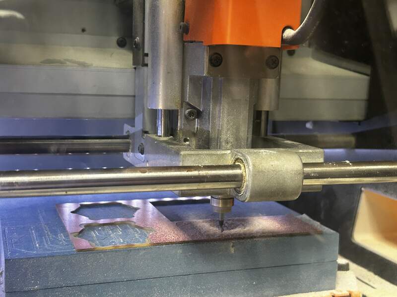
- Bring the folder onto the machining PCs local drive
- Open machine and brush away dust on the bed so you have a clean surface to mount your PCB milling stock.
- Mount your PCB milling stock with the double sided adhesive tape
- Remove your endmill with the Allen wrench and put in a [1/64”] flat endmill finger tight in collet.
- Set your X and Y origin through the control software.
- Decrease rapid move settings and bring you endmill down slowly till it is close enough to just start to burnish the copper PCB surface when you rotate the endmill manually and set you z in software.
LMC → cutdelete any files currently loaded in the dialog and add in your first machining file which should be your traces initialize operation and close protective shroud.
04 — Soldering + Testing
BOM
- x2 1208 White LED : 3.1 forward voltage .25 W consumption [datasheet]
- x2 Tactile Pushbutton
- x2 1208 10 Ohm Resistor
- SMD 2.54mm Header Pins
- x1 Xiao ESP32 C3
Soldering workflow
- Visual inspection of PCB. Since it is a simple PCB I can see if shorts are present.
- Gather your components
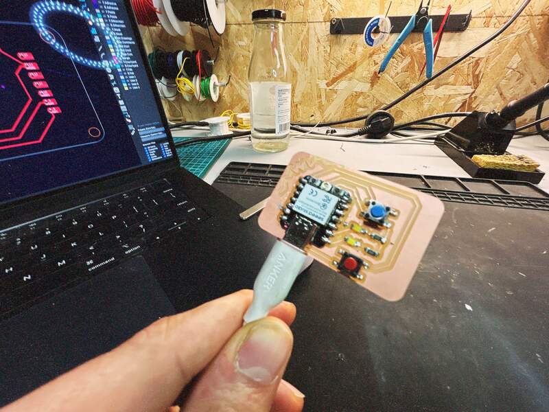
- Solder smallest components first from center of the PCB outward. This meant I started with the LEDs first applying solder to one of each of the SMD LED pads. Then I held the LED down with Tweezers and soldered one of the LED pads down then I solder the other side down while holding module with tweezers. This basic process was repeated for all SMD components.
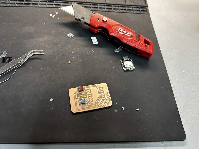
- Code was loaded onto Xiao (code is below) and ran with Xiao was connected to PCB female header pins.
const int button1 = 8;  // Button connected to pin 8
const int button2 = 9;  // Button connected to pin 9
const int led1 = 0;     // LED connected to pin D0
const int led2 = 2;     // LED connected to pin D2

void setup() {
    pinMode(button1, INPUT_PULLUP); // Use internal pull-up resistor
    pinMode(button2, INPUT_PULLUP);
    pinMode(led1, OUTPUT);
    pinMode(led2, OUTPUT);
}

void loop() {
    if (digitalRead(button1) == LOW) {  // Button is pressed (active-low)
        digitalWrite(led1, HIGH);
    } else {
        digitalWrite(led1, LOW);
    }

    if (digitalRead(button2) == LOW) {  // Button is pressed (active-low)
        digitalWrite(led2, HIGH);
    } else {
        digitalWrite(led2, LOW);
    }
}
05— My results
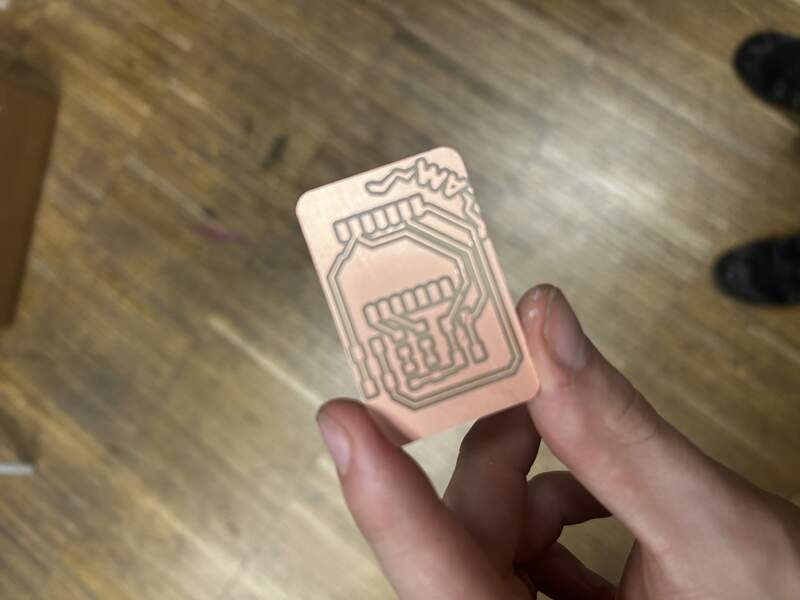
I had to do two versions of my PCB from a soldering error on the first PCB. To save time I was using the castellated pins on the Xiao to solder directly to the PCB instead of using female sockets. This was a mistake because the XIAO has pins on its underside and these were shorting across the exposed copper on the PCB. I had actually anticipated this and was planning to add tap underneath the Xiao to Isolate it from the copper PCB, but I was working quickly and forgot to do this. Instead of desoldering I decided to remake the PCB. Ultimately, from this experience I will never use castellated pins unless it is an explicit design requirement.
For both PCBs I had no issue milling the traces, but many issues trying to initialize the profile milling operation. I spent an hour trying to work this out the first time and figured out it was simply the Mac OS to PC file transfer on the portable drive. Basically it was doubling the files and creating a copy of each machining file that was a larger size. This larger copy was some kind of artifact and it was just the smaller version that was the usable copy.
06— Volt_Jig for Fast Multi Voltage Testing
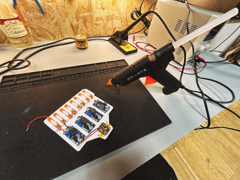
This was a quick personal project I made to test out different actuators I am looking at using for my final project. In the past constantly switching between different voltage when testing different output devices is a pain so I wanted something that could provide 4 of the most common voltages I use. If this is something I end up using a lot (I think I will) I will turn it into a custom PCB version. For now Though I am quite happy with how it turned out.
Project Files
