06— Electronics Design
Assignment
- Group assignment:
- Use the test equipment in your lab to observe the operation of a microcontroller circuit board (as a minimum, you should demonstrate the use of a multimeter and oscilloscope)
- Document your work on the group work page and reflect what you learned on your individual page
- Individual assignment:
- Use an EDA tool to design a development board that uses parts from the inventory to interact and communicate with an embedded microcontroller
00— Initial Thoughts
Early this year I spent a couple weeks working in Fusion’s electronics workspace to develop a custom Xiao based stepper control board. Part way through this process I decided to switch over to Flux.ai because it solved the issue of having to create and source items for my own custom library of components.
What I had designed was essentially a carrier board to hold a TMC 2209 stepper driver, Xiao, a Meanwell LED dimming module, and 3.3V regulator module. I think it took me three weeks to design and even though (I thought) I was very careful during the design process I made some critical mistakes. This included reversing the polarity of the electrolytic capacitor... I also think I forgot to check some critical box when ordering the boards that excluded flux paste to the board. Whatever I did the resulting PCB was extremely difficult to solder components to. So all of that said, I never got around to fixing the mistakes in this PCB design. I ended up getting the board working with a lot of additional splicing between point and a ton of troubleshooting. One of the reasons I was interested in this course was precisely to sort out how to make pcbs and figure out how to design some crucial circuits.
So I carried this knowledge going into this week. In PCB design my goals are not around price cutting, miniaturization, or producing something super optimized. What I want to learn is efficient board design that allows me to add high quality prebuilt modules and components in a reasonable footprint size. That said, I do want to design all of the regulated voltage rails because I want all of my projects to function with USB C PD which presents some additional challenges. Specifically I am pretty sure in most cases I have to work from a starting voltage of 20V if I want to use the whole common 100watt capacity of the PD protocol. So if I can develop a board that can convert down to 2/3 voltages off of 20V input I will be pretty happy.
01—Group Project
It was useful for me to get to know how to use an oscilloscope for this weeks group project. I have considered buying one many many times I just never got around to choosing the right one because there are so many options. I now see that even a a very basic oscilloscope is useful for trouble shooting and wish I would have picked up one a while ago. When (or if) I get back to my home shop that will be the first new tool I will buy.
02—Terminology and Best Practices
Best Practices
- Coupling capacitors should be as close to the pins they are supplying as possible. This decreases parasitic inductance.
- Ground on board should be common unless you have a very specific reason for it not to be. I think a use case might be audio amplification to avoid noise(?)
- Common trace widths are used and there are limits based on the manufacturer design rules.
- Route high frequency tracks first… these sometimes need to be impedance matched ie. the same length.
- Do not place copper underneath an Antenna. Use a ‘keep out’ pad to exclude the copper fill.
- Avoid 90 degree bends at all cost.
- Castellated pins will let you solder a PCB to the PCB without headers.
- Net portals keep the schematic organized by using a kind of tagging system that links circuit paths together.
Key PCB terminology
About list: List was taken from chat GPT “what are the 20 crucial PCB design terms to know”
- Trace Width – The width of a copper track on a PCB, which affects current-carrying capacity and resistance.
- Air Wire – A visual guide in PCB layout software showing electrical connections between components that still need routed traces.
- Via – A plated hole that connects copper traces between different layers of a PCB.
- Blind Via – A via that connects an outer PCB layer to an internal layer but does not pass through the entire board.
- Buried Via – A via that connects internal layers of a PCB without extending to the outer surfaces.
- Pad – The copper area where component leads or pins are soldered onto the PCB.
- Annular Ring – The copper ring surrounding a via or pad, necessary for reliable soldering and electrical connection.
- Copper Pour – A large contiguous copper area on a PCB, often used for power or ground planes to reduce noise and improve thermal dissipation.
- Silkscreen – The printed text and symbols on the PCB surface used for labeling components and reference designators.
- Solder Mask – The protective coating on a PCB that prevents solder bridges and oxidation, typically green but available in other colors.
- Netlist – A list of electrical connections between components, generated from a schematic and used to verify PCB layout.
- DRC (Design Rule Check) – A verification process that ensures a PCB layout meets manufacturing constraints like trace width, clearance, and hole size.
- Clearance – The minimum spacing between conductive elements (e.g., traces, pads) to prevent shorts and ensure manufacturability.
- Thermal Relief – A design technique where small traces connect pads to a copper pour, helping with soldering and reducing heat dissipation issues.
- Gerber File – A standardized file format used by PCB manufacturers to produce circuit boards, containing layer information like copper, silkscreen, and solder mask.
- Teardrop – A widened trace connection to a pad or via, used to improve mechanical and electrical reliability.
- Keepout Zone – A defined area on the PCB where no traces, components, or copper pours are allowed, typically for mechanical or clearance reasons.
- Impedance Matching – The process of designing traces with specific widths and lengths to control signal integrity and prevent reflections in high-speed circuits.
- Stitching Via – A set of closely spaced vias used to connect ground planes, reducing EMI (Electromagnetic Interference) and improving signal integrity.
03—KiCAD Software
About section: I liked the workflow of KiCAD quite a lot except for the switching between the 3 windows. I found the 2D design system to work similar to adobe illustrator. This was my main gripe with Flux which despite being a simple interface can make some pretty normal seeming things pretty difficult. I see myself using kiCAD when I need more advanced features.
KiCAD Fundamentals
Core workflow
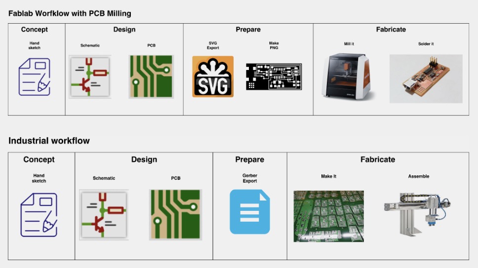
- Pull Components out of the ‘fab’ library
- Design initial schematic
- Position parts to consolidate footprint and drafting traces as you go ↔ reposition redraft
- Check 3D
- Export into usable formats for production
Keyboard shortcuts
rfor rotate
cmd +lfor portals
afor searching in part library
- When working with MCUs only reference absolute pin names not the numbers arbitrarily associated with them.
- Use only components that use the 1206 package style or similar SMD size when you can.
- Alway open from project menu never individual KiCAD project files
PCB Design rules for in house production
- Clearance - 0.4 mm
- Trace width .35mm
- 1/64” milling bit for traces
- 1/32” for holes and edge cuts
Designing A Simple LED Toggle board
- Started designing PCB in KiCAD. I first created a new project through the home page that pops up.
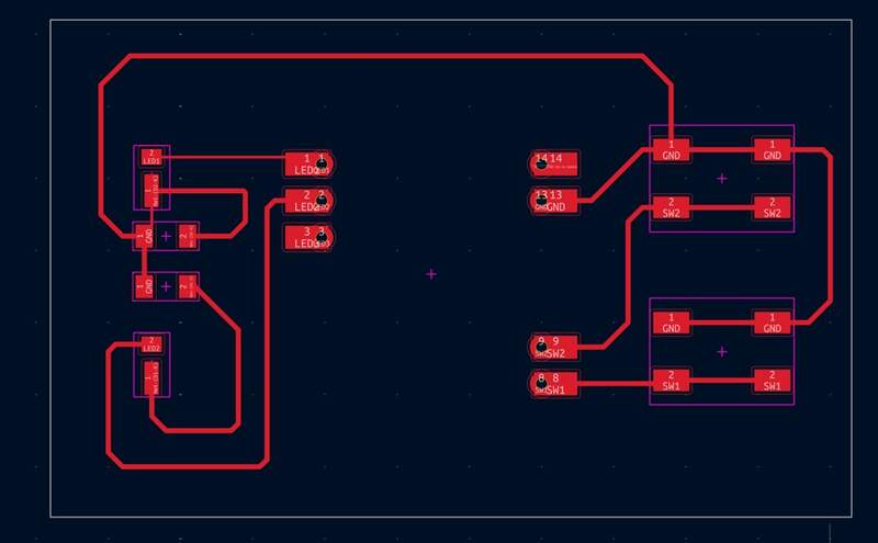
- Quickly ideated about some concepts. I settled on creating a multi voltage buck converter that could output 3.3/5/12 volts… Then I decided this was too ambitious and instead opted to just create part of this project. The part I am focusing on is very simple. I am creating 3 LEDs and 3 switches. Each switch will be able to toggle the state of its corresponding LED.
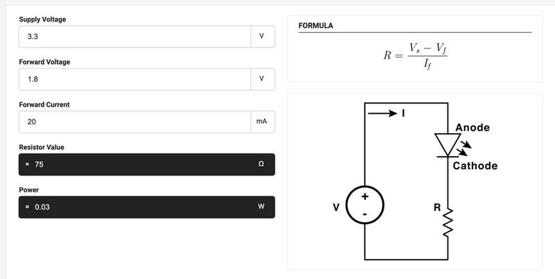
- The SMD LED I chose notes in its datasheet that it operates best at a nominal voltage of 1.8V. Below I used a calculator on Digi-Key to calculate the size resister I needed.
- After a quick google search I found that all IO pins on the Xiao can pull up or down their input pins. This means I don’t need a resistor on the button pins to keep the button input on the Xiao from floating.
- I quickly mocked up the circuit then when I looked at it in the footprint I realized that I should distribute the elements on left and right to make routing easier.
- I checked the design DRC rules in board setup to make sure the design was compatible with our milling process.

- I realized after looking at the inspection panel below all of the nets were drawn at the wrong width. Since I could not figure out how to modify them globally, I redrew all of the nets at the correct .35mm width.
- I realized that the Xiao footprint I was using had a lot of extra complexity so I did a quick google search and figured out how to delete the element by going into the library editor
cmd+e.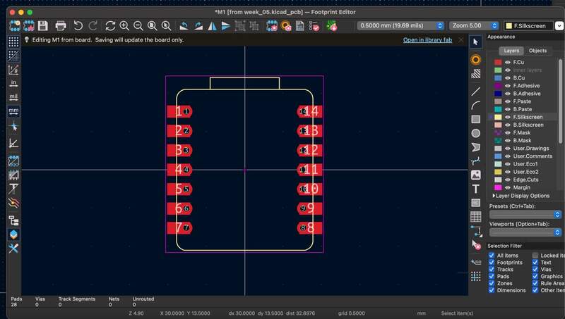
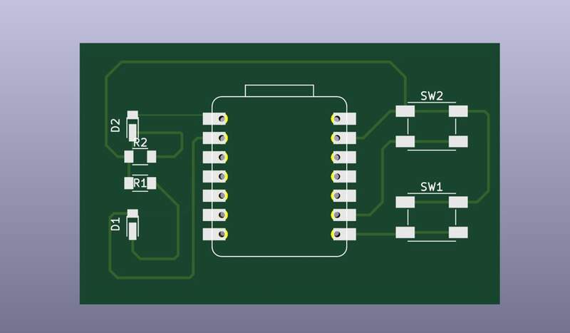
- Below is a rendered version. I decided to add back in all of the Xiao traces because as Adai pointed out I would actually be connecting it with a set of female sockets.
- Run DRC (design rules check)— When I did this I received 14 errors. Upon inspection of the actual errors none of them appeared to be critical.
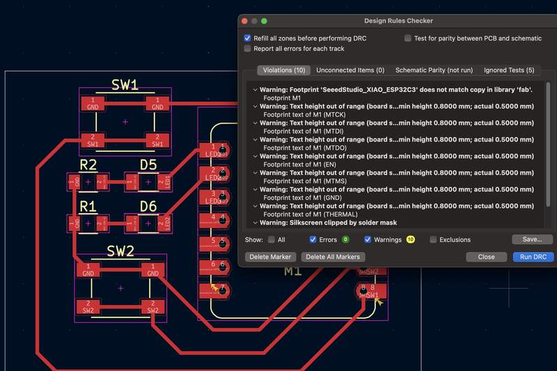
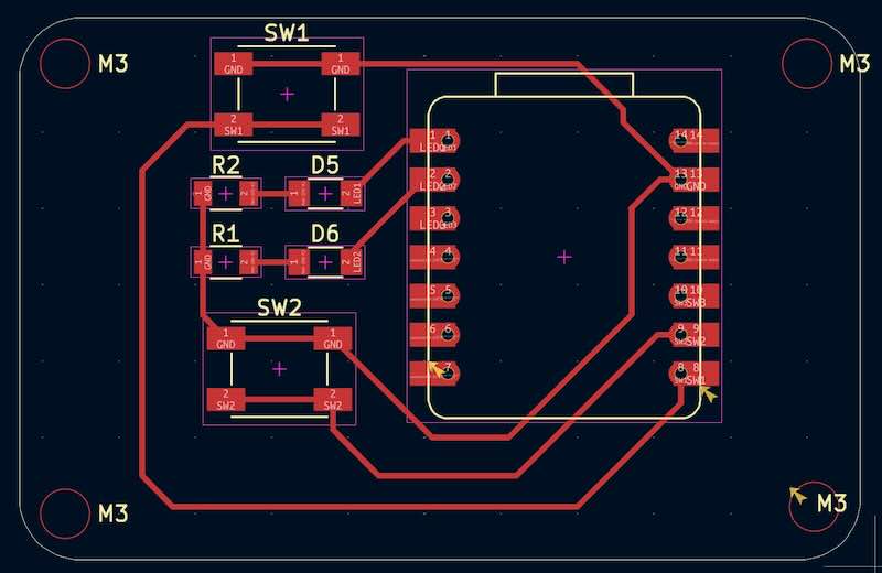
- To fix the errors I went back and edited the Xiao footprint. I did not realize that there is both a local library for the project and a global library (ie. fab library). I deleted unused pads from the local footprint. All warnings were removed except ones pertaining to the silkscreen overlapping with the pads which I am assuming could be fixed during export.
04— Flux.ai PCB Design
About section: Man I wish I had actually written notes when I worked in this software the first time. Somewhat ironically Flux is almost a command line workflow where you leverage a lot of properties and rules to set up your board. In some ways this make anything that isn’t super basic pretty challenging compared to KiCAD. If you utilize template though you can eliminate some of this leg work. It is the search engine for component and circuit designs that make this software worth it for me.
Core Flux Shortcuts
- Rotate component ‘[’ r ‘]’
- Invert net elbow ‘f’
- Cycle through trace widths ‘w’
- Quick grid align ‘s’
Creating a Part from Scratch… trivial
Part creation is an… extremely painful process and there is very little documentation on it so some of the process I came up with as I went. I think people are creating footprints in KiCAD and importing them. It feels like doing graphic design with an etch a sketch.
- I know my final project will use an Adafruit USB C PD trigger board this handle all of the USB PD and lets me run everything off of a 100 W max USB C power supply (if I have it set to its 20V output).
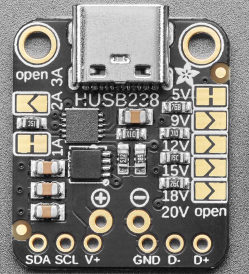
- Creating the symbol — I need to generate an SVG for my custom symbol. Workflow is: Step file → into fusion → generate DXF → place DXF in adobe Illustrator → remove unneeded lines → join edge lines into compound path → set lines to pure white and 1px with no fill color→ export as .SVG
- Open Flux.ai file create and name all of your terminals that you want to be represented in the schematic for your PCB. Name your file and and choose properties that will help people find your board [manufacturer, datasheet, etc.]
- Deselect everything and scroll down to the assets panel. Import your SVG.
- Click file dropdown
publish to librarythis imports the symbol into the public searchable library.
- After it has been imported to the library open a new Flux project file import your custom library symbol you just saved by dragging it from the library into your workspace. Set its position input to [0,0].
- This is where things get confusing. You have this second Flux project open as a dummy document. You need this because the custom symbol will not be visible otherwise. Now place and name the terminals you need on this newly created symbol that you can view because it is in a new document. Great, now you have placed all pins where you would want them to be.
- Now go back to original file used to create the library file. Copy positions numbers of newly placed items to
pin positionfield exactly for each pin coresponding pin. Now update the library item by clicking library publish in file drop down… You now have symbol linked to pins in the schematic workstation.
- You now just have a custom symbol. Not something that is strictly necessary, but useful visually. Add additional assets like your 3D file in .stp and a .jpg thumbnail. Click on the newly imported .jpg to add click
add thumbnail.
- Next step is to create your footprint. For this you need to go to click the PCB workspace tab.
- In essence you are a pick and place machine. You need to place your outline in +x +y space. This means you are working in the top right quadrant in the coordinate plane with the lower left corner 0,0 as your refference. This allows you to measure all of your hole locations from hole center to the bottom left of the physical PCB.
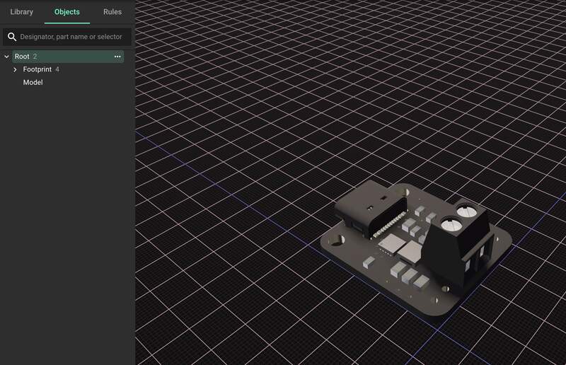
- Something important to note is that I don’t think you want a layout item for the PCB layout (creates the PCB profile) if you already have a CAD model for the part. This creates overlaying 3D PCBs which is obv. not ideal representationally when you working with the 3D file.
- Another important note. Most PCBs are designed around very regular mm based intervals (typically 2.54mm or multiples of this) when designing the 2D PCB footprint you can leverage this as a sanity check when you have to measure from circle center points with a pair of calipers.
- From that same board design workspace click the add model add in from the layers panel → select asset class and select the .STP model you imported. Switch to the 3D mode in the board design workspace. Use the arrow keys on your keyboard to position your 3D model. If you need to rotate it add rotation underneath the asset class where the model is selected.
Flux Buck Regulator Tutorial
About sub section: Something I am always needing in an electronics projects is a simple way to get several line voltages to use across different modules. I know this will be needed for my final project circuit so I will probably use this circuit as a reference to design the power section of my custom PCB.
- Discussion of terms linear vs switching regulators + related components
- Quick chat GPT query confirms that using a linear regulator is really not advisable most of the time. This is because they are typically not very efficient (efficiency is supposedly as low as 10-50%!). They do have the benifit of requiring less components in a circuit to be operational.
- Switching regulators let you step up, step down or invert the voltage.
- Other components I ran out of time to do research here, but two capacitors some resistors and a coil are used to complete a basic switching power supply design.
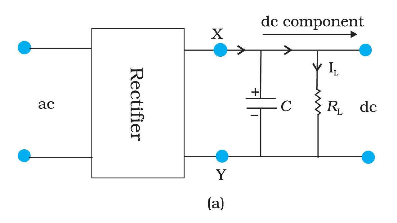
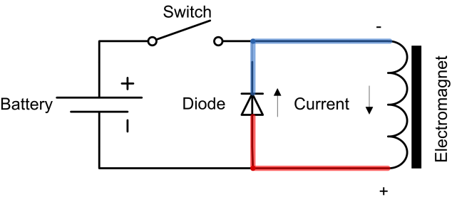
- Catch diode is used in a buck converter (switching power supply) circuit when its switch is open. Not totally sure about the operating principle, but the inductor holds current then releases it as back EMF (?) when the switch is open letting it pass through the diode and separating it from the power source in that brief interval. A capacitor is typically present as well.
- Add a description in the description pane of the inspect panel. Also add additional properties. The built in copilot can leverage this information to make part suggestions based on project requirements.
- Properties → add → max output voltage
- Properties → add → max input voltage
- Properties → write custom string → max output current
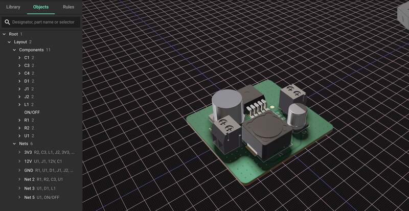
- Add in LM2596 buck converter component (LM2596DSADJR4G). You can ask copilot directly what the chosen IC is capable of and what its pinout is. You can take a photo of a schematic and paste it into copilot to have it tell you what each component does. The teacher just creates a circuit exactly from the reference schematic found in the data sheet with the exception of the feedback resistor that controls the output voltage.
- I went to the finished project page and started populating my blank page with the specific components by copy and pasting them into my project.
- For the official components like “generic resistor” you can select the package style in the dropdown menu in inspect column.
- One of the feedback resistors that sets the current needs a weird value the instructor just chooses a near value for the resistor based on a chart of commonly found resistance values.
- Making all of the connections. I copied all of the connection detailed.
- Power Net portals were used for v+ I think these just differ visually from regular portals.
- Copilot can be used in the workplace for more contextual recommendations by right clicking and selecting a copilot option.
- Adding global design constraints—Switch to PCB workspace… in the objects side panel you can select individual traces and add rule sets. Four layer stack up is set as the default rule set in the dropdown under
layer rules. This panel tells you all of your PCB defaults.
- Rename all of your power nets so they display the voltage they carry.
- Add
trace widthunderobject specific rulein the inspect panel to both your 12v and 3V3 nets. Set trace width to [80mil].- I used PCBway in the past and they had good customer service JLC is the other popular Chinese option that I know other people like. Flux has built in templates that contain PCB manufacturer rule sets that you can use.
- You can ask copilot to recommend trace widths.
- Under
rules→add rulesetyou can add a selector based global rule set. Here we add the string to the selectors ‘nets’ and then select the preferred trace width in thelayout rulessection. We simply type the net width we want to default to which are10mil 20mil 40mil 60mil 80mil !important.!importantdisables the default rule
- The specific Syntax for selector based rules can be found here.
- Orient and place component on PCB— I moved and rotated
‘[’ or ‘]’components into position then double clicked labels and rotated them so the were legible and visible.- You can use the 3D view to identify orientation of female inputs.
- This generates an individual ‘rule’ for each component that changes the orientation of the label when you do it through the interface.
- Create PCB size using layout in object panel. If you need to move the components into position you can select all of them through the objects panel excluding the ‘layout’ directory header folder.
- Routing Nets—
wlets you select between trace widths.
05—Learning KiCAD Again….
About section: After moving into Flux I realized I actually really need to know KiCAD in order to make footprints for flux parts. This is all in the spirit of saving time?
Schematic workspace
- Looking at the schematic workspace I feel I have an understanding of the essentials. I think I am missing some of the specifics of some of the wire joining functions for specific, but common scenarios.
- There is a workflow where generic components are used first then you link footprints in the schematic workspace so that the schematic transfers over to the PCB footprint designer seamlessly. I understand why this could be a more flexible approach if available components change. For my purposes I think I will always try to work with items that have all assets included.
Questions
- PWR Symbols — I think I should probably just use these instead of global labels?
- Sheet pins
- Hierarchal sheets
- Wire to bus
- Place junctions
- Place sheet pins
Things I Learned
mwill let you just move the whole component upon selection
- Highlight wires button for displaying connected components
- Properties box for showing you what modification options you have
- Find and replace for quick renaming
Footprint Workspace
- Ok yes, again this feels very logical with view modes and special tools for specific routing kinds.
Questions
- What role does every layer on the PCB serve?
- How do I select a whole trace and not just a part?
Things I Learned
- The PCB layer you are drawing on is noted at the top
- Update PCB can be used to only push recent changes so elements could be added to the schematic and than they will show up delinked to the footprint.
RC + 'select all tracks in net'lets you modify the whole net
- The track dropdown in the top left changes the drawing width for your tool, not the selected track.
board setup’constraints’ and ‘predefined sizes’ seem to be the most important for my needs. Constraints does not seem to constrain all further actions, but will merely flag slip ups in the DRC I think?
-
predefined sizesadds different track widths to your top left track dropdown
- Properties panel toggle in the bottom left is really important just leave it open this give you all editable properties for a given selection.
- Appearance panel is really useful for dimming and isolating different sections
Interactive delete toolis a lot more convenient to get rid of unwanted elements
- Components can be moved to the back layer by right clicking and selecting that option.
- There is local level footprint editing and by project footprint editing. In my case I needed to remove pads for the Xiao I was using at the local level.
06— Notes From Class: Common Components and circuits
Most Common Capacitor Use Cases
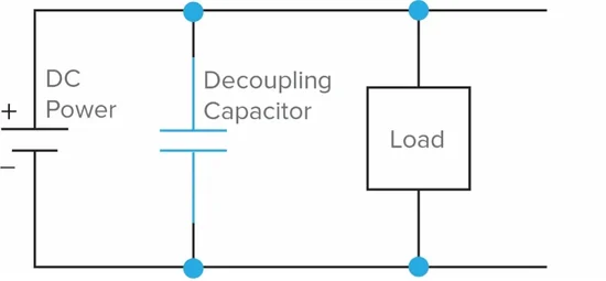
- Decoupling caps
- They will discharge at the voltage that is used it capacitance value will dictate how much of a dip in voltage it could smooth out.
Diode
07 — Final thoughts and Directions
Happy with how thing went, but there are some things I need to look into.
- I need to go back and figure out how to port footprints from KiCAD into Flux.
- I want to understand role of each component in the buck converter design I did.
- I will need to figure out how to properly rout impedance matched signal wires for I2C connections
- I want to have a better grasp on the PCB layers and what they do as well as manufacturing as well as what design rules are relevant to the kind of PCB manufacturing I plan to outsource.
Files
For flux files search Adafruit HUSB238 USB Type C Power in library or go to this link.
