week 6 Electronics Design
Group assignment:
- Use the test equipment in your lab to observe the operation of a microcontroller circuit board (as a minimum, you should demonstrate the use of a multimeter and oscilloscope)
- Document your work on the group work page and reflect what you learned on your individual page
Individual assignment:
Use an EDA tool to design a development board that uses parts from the inventory to interact and communicate with an embedded microcontroller
Summary:
The group assignment involved learning to use lab equipment like oscilloscopes, multimeters, and potentiometers to analyze a microcontroller circuit. The team documented their work and learned PCB basics with KiCad. The individual assignment focused on designing a development board using KiCad, starting with an ESP32C3 microcontroller, LED, and resistors. The process included adding FabAcademy libraries, defining pinouts, creating schematics, and ensuring proper connections. The design was refined in the PCB editor, checking for errors and applying design rules. Additional features, such as I2C communication and power connections, were added. The final board was prepared for fabrication, with best practices like using resistors as bridges and filling zones for grounding.
Group Assignment
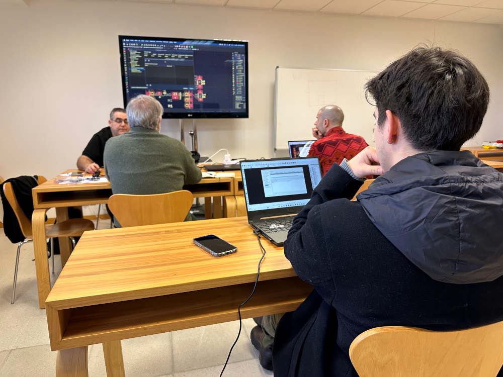
On Thursday, Luis came to our lab to tought us abot the basics to do a pcb, so in the morning we were learning about KiCads and electronics structure, components, how to build a pcb, etc. Everything is documented above. And here is a pic of us learning some new stuff.
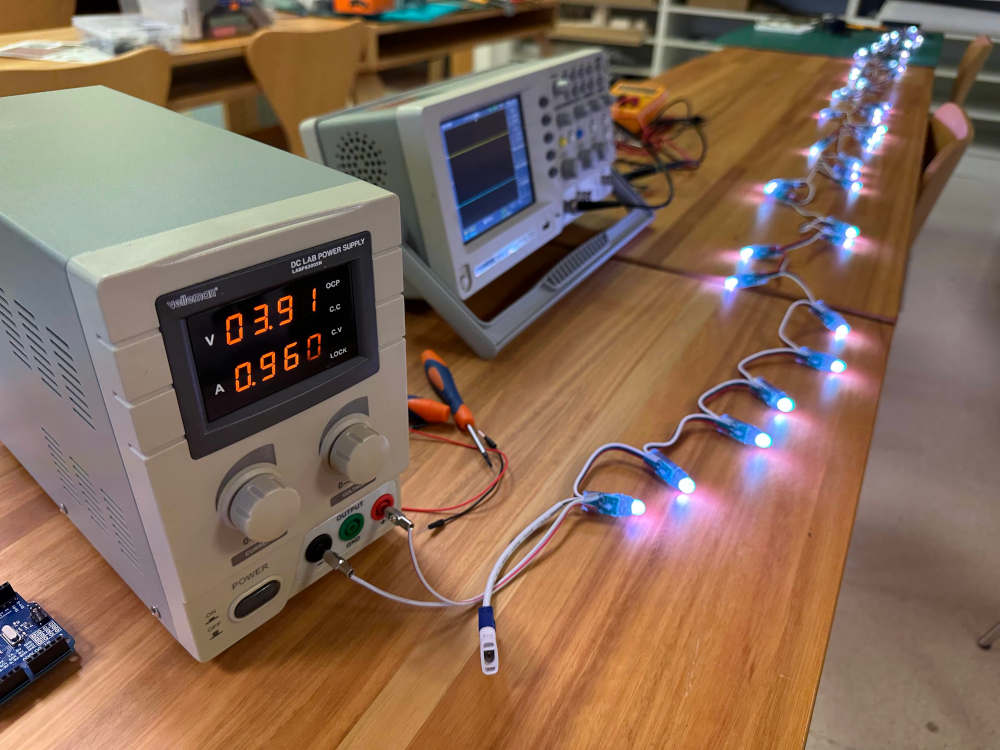
By the afterrnoon, we figured out how to use three instruments crucial for our projects in the future: oscilloscope, multimeter and a power supply.
Specifically Pepe needed to know how much current some led lights needed and actually if they were working. Here a pic of how the circuit was built.
Individual Assignment
KiCad
My first project
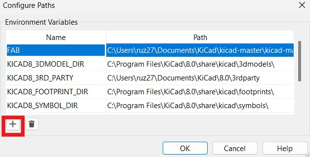
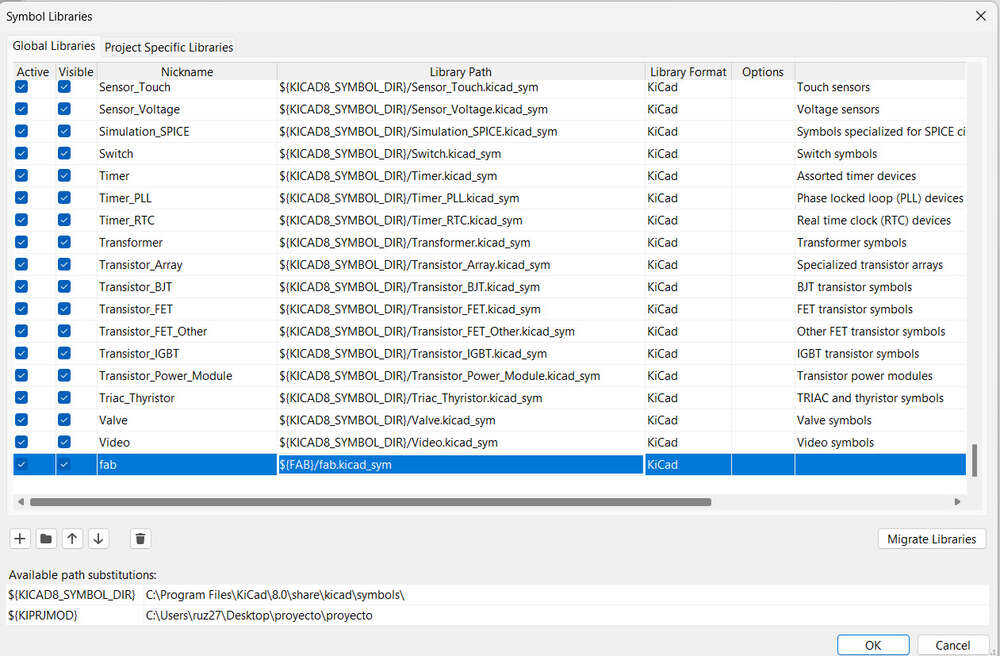
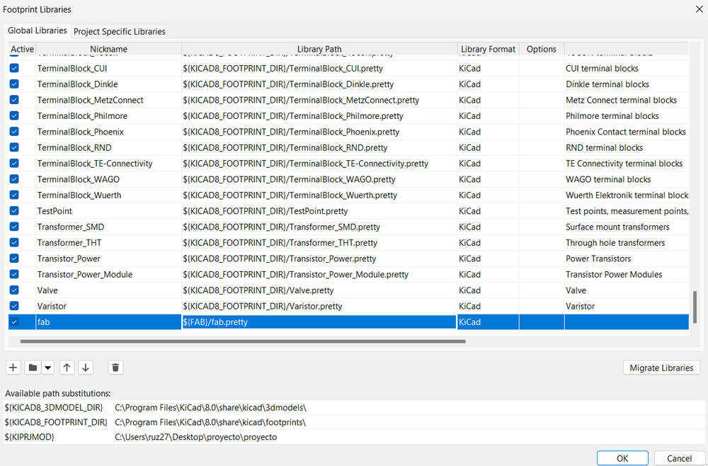
First we add the fabacademy libraries from the fabacademy page:
Add the path envirnoment.
To do the most basic board ever. I add the microcontroller ESP32C3, led light, resistence,
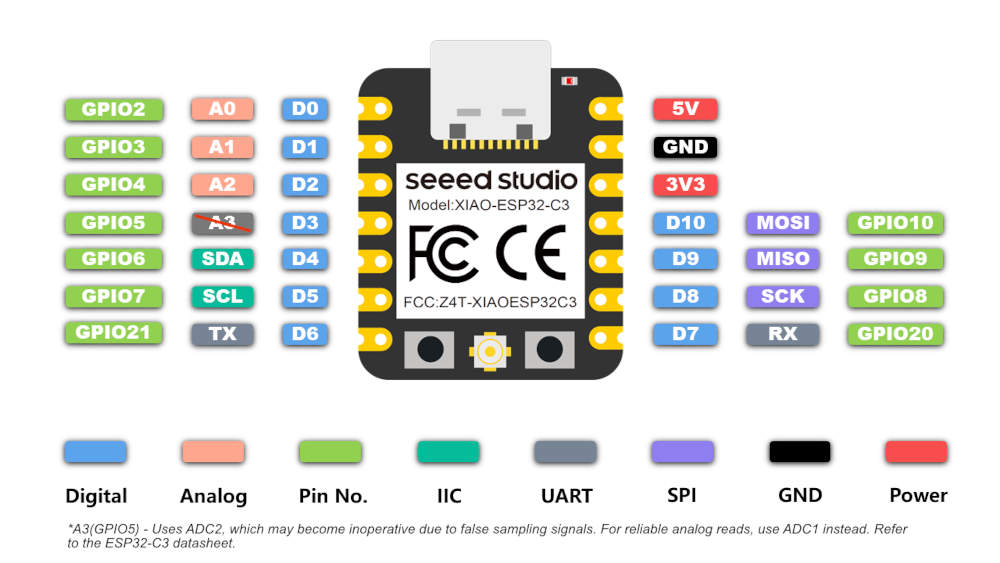
Here is the gpio because its important what is each pin of the microcontroller.
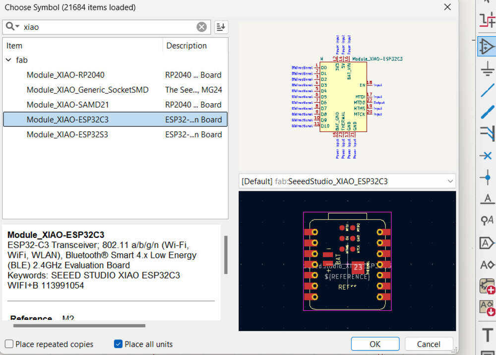
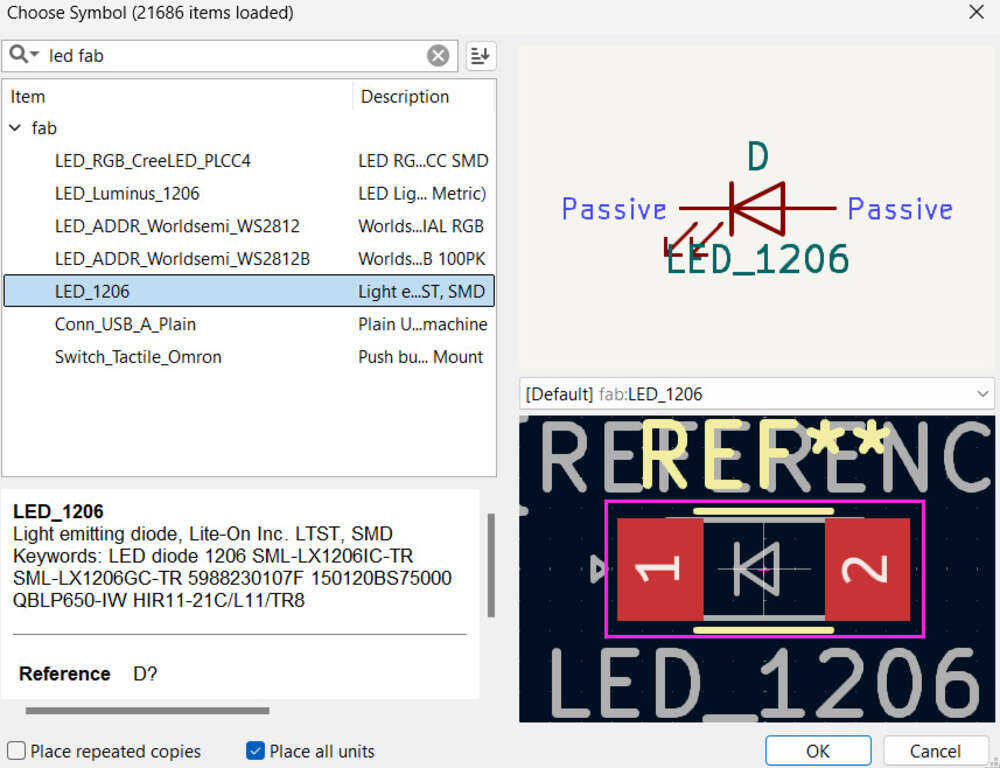
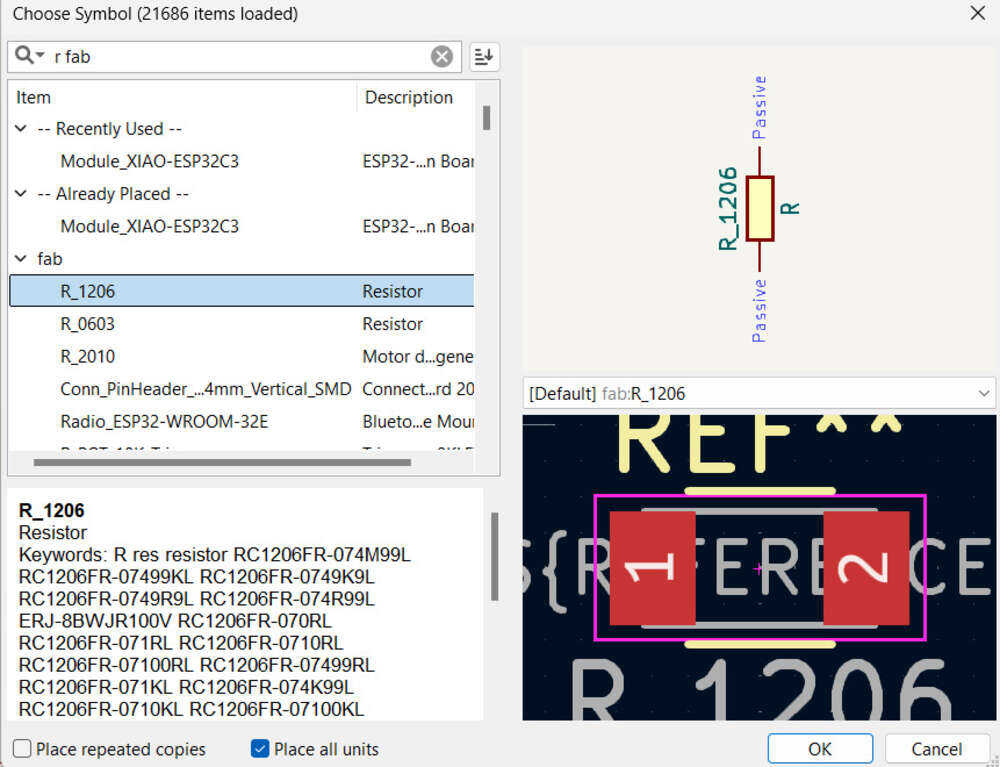
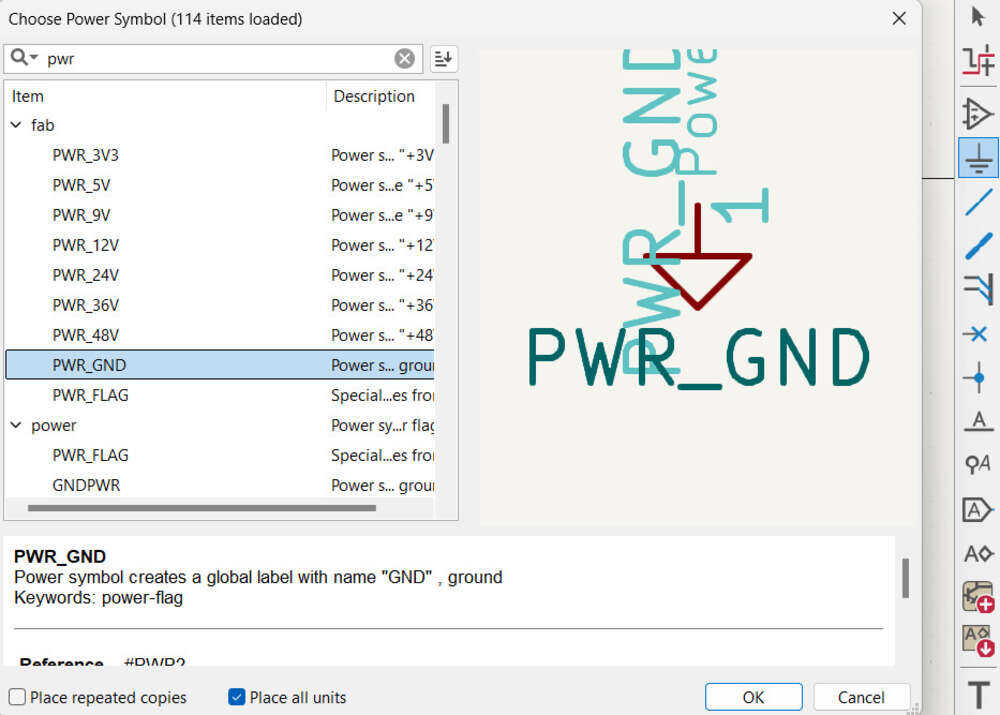
Change the names to the ones you want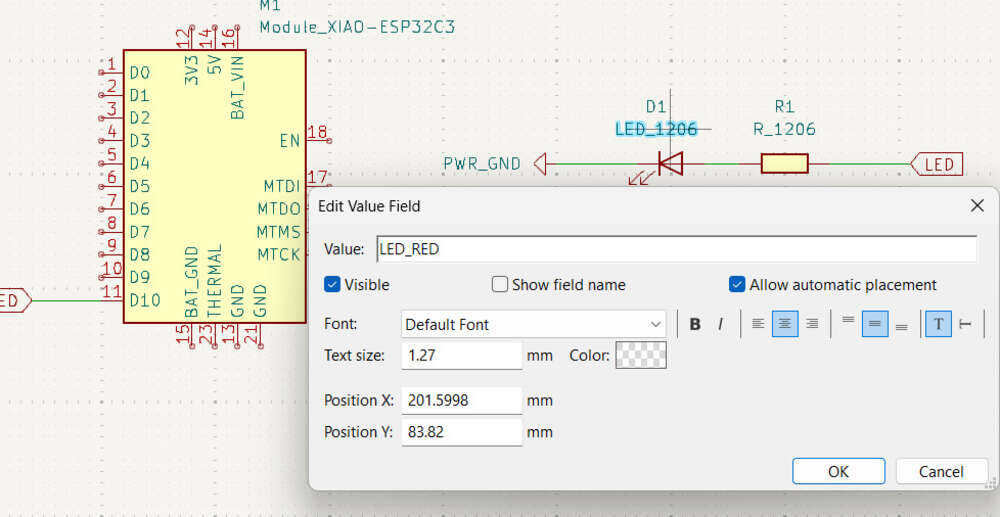
Put the etiquetes and connect the pins to the board. Here is important to see the Pinout to know what is exactly waht pin.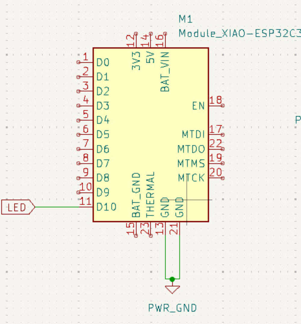
It is important to check the program if it is correct or you have to changes. I lost the screenshot I took were the erros were shown. Although, this erros said that there were “free pins” that were nor connected.
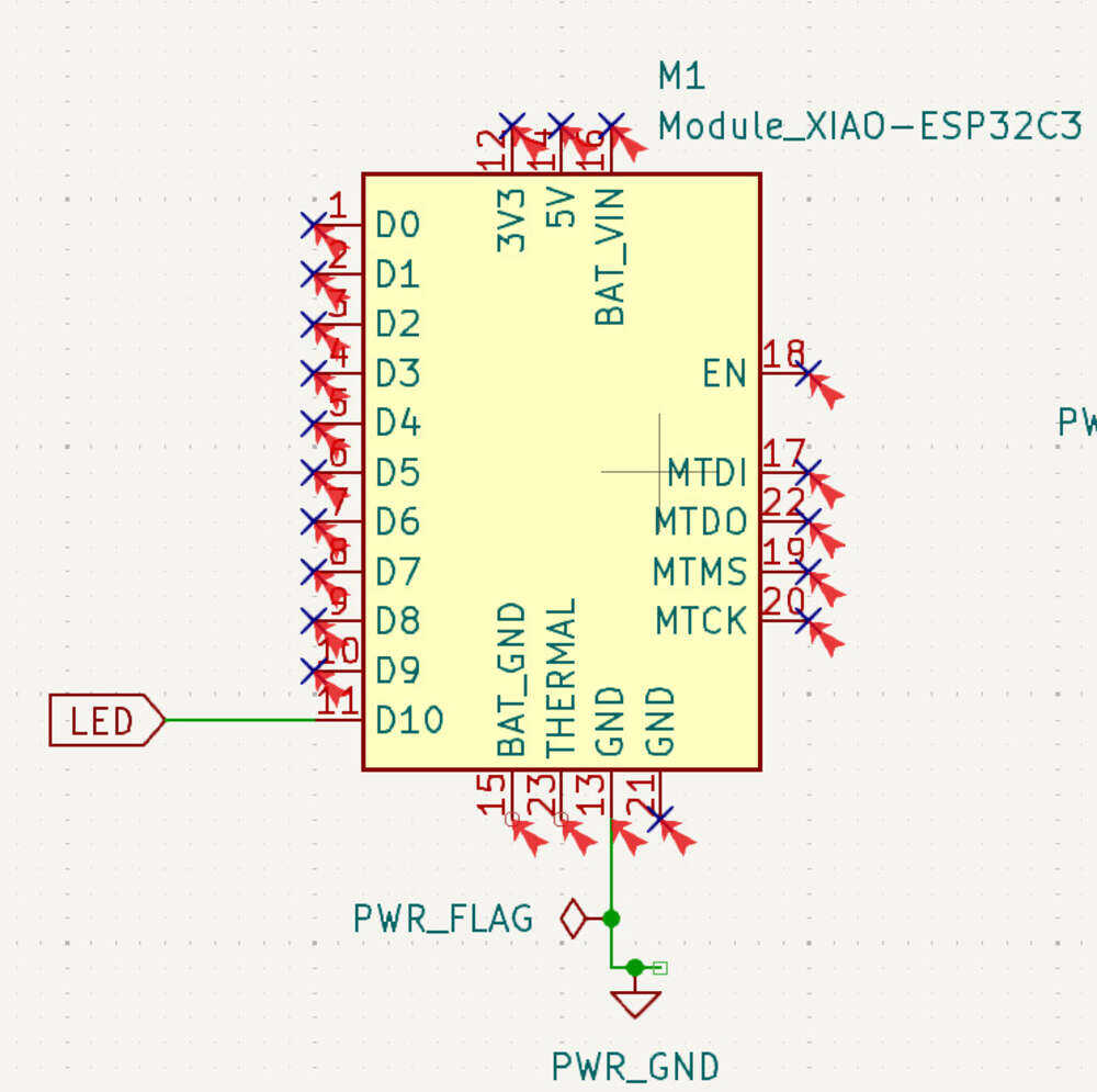
If there is a gnd pin not connected it will have an error so you have to close all or connect it to the pwr_gnd
This is the general schema of the circuit.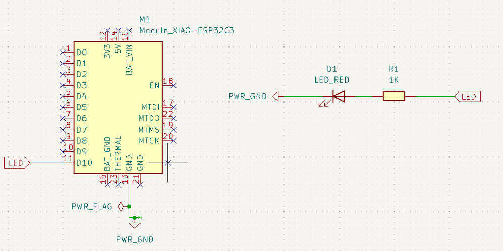
Then you have to go to the pcb editor and upload the schematic image you did. Here is when you do the architecture of the pcb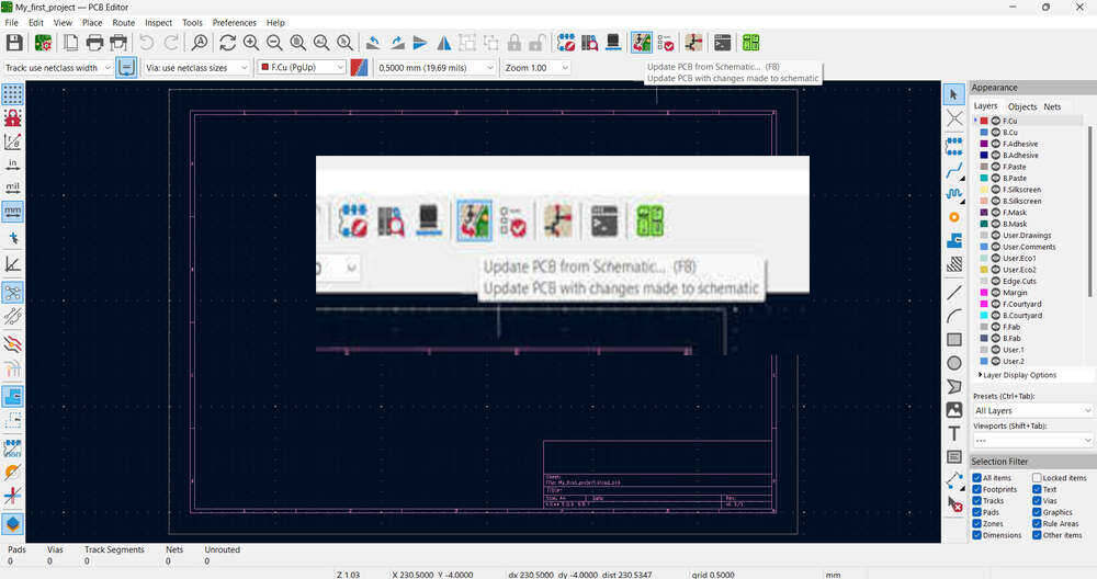
Be sure there are no warnigns oe errors.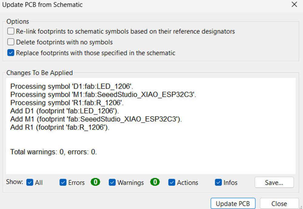
Here you can see board and in this option you can change some settings.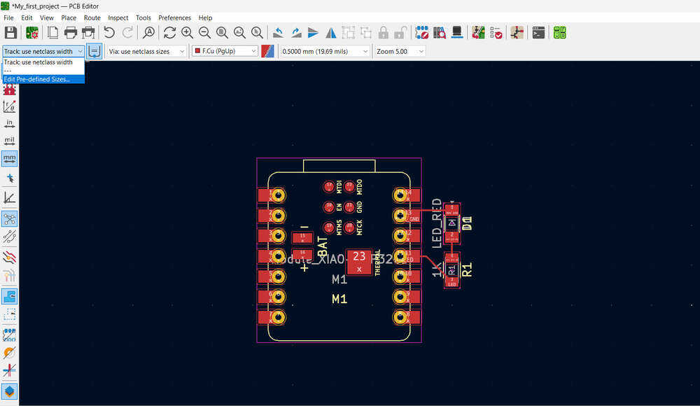
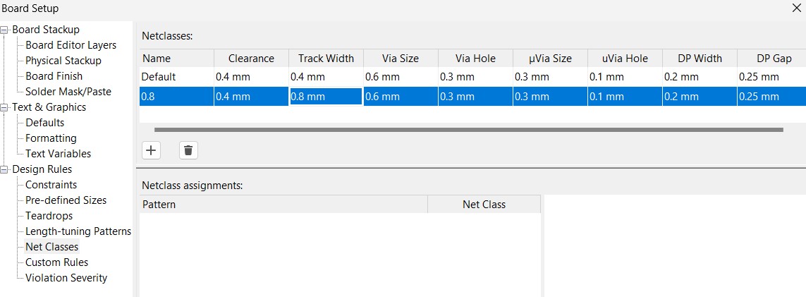
Be careful with the size of the cables.
Check the design rules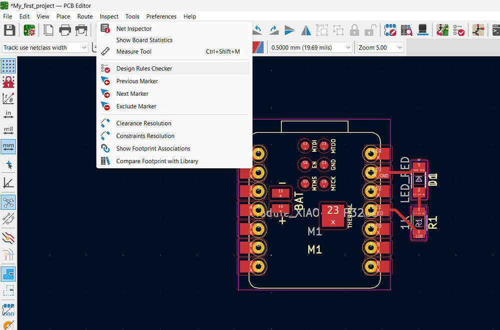
Then, you have to draw the contour of the board.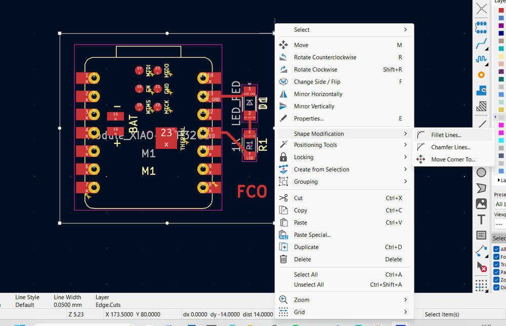
Now is ready to export on .gbr(for fabrication) or .svg(to mill)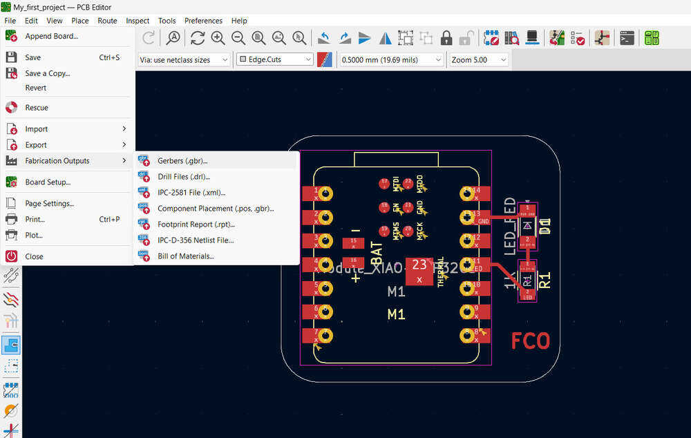
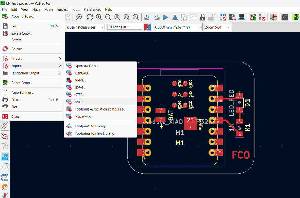
In china they produce millions of pieces that people sent the .gbr
Edge cuts and inter on different layers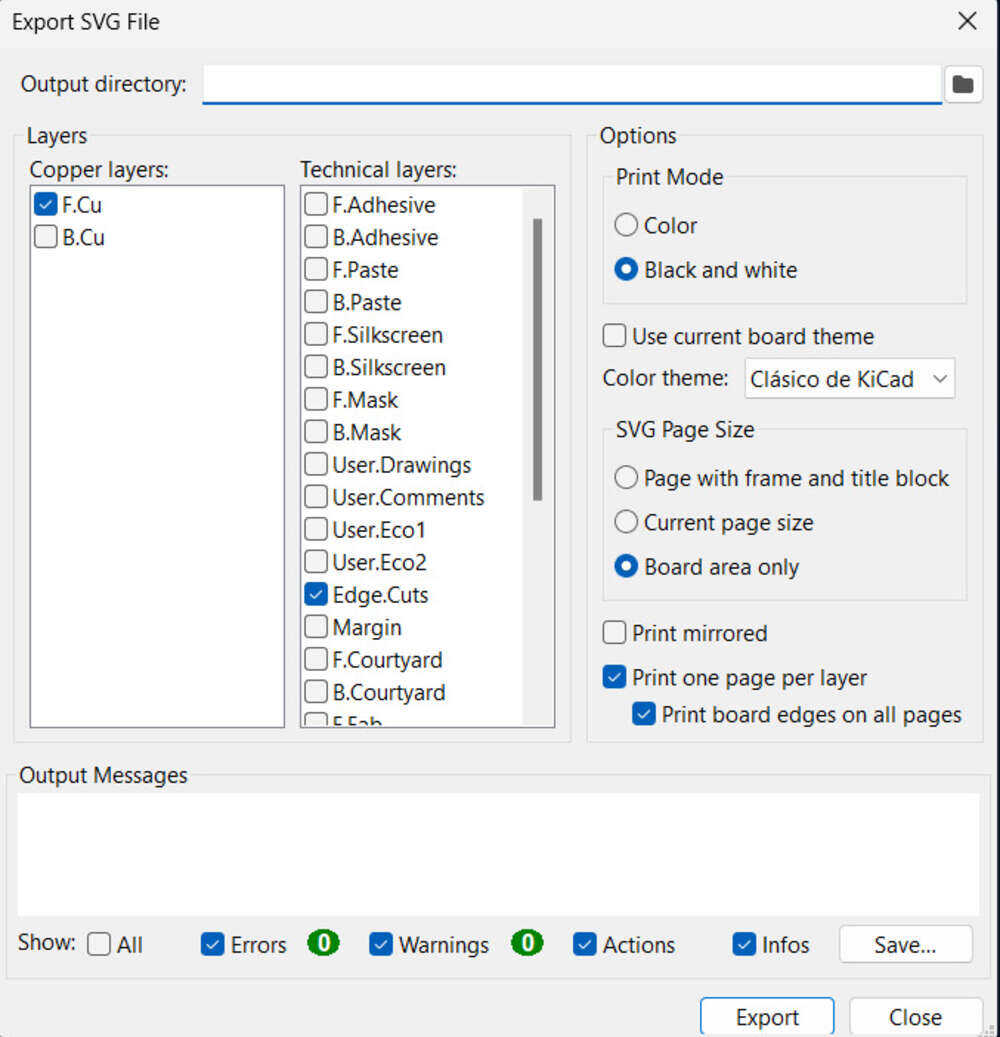
PCB for my project
For this assignment we can use the board we did and modify so not to start from skatch.
we add a pinsocket with 3 pins horizontal is that it goes paralel to the board direction. This couls be a Temp sensor.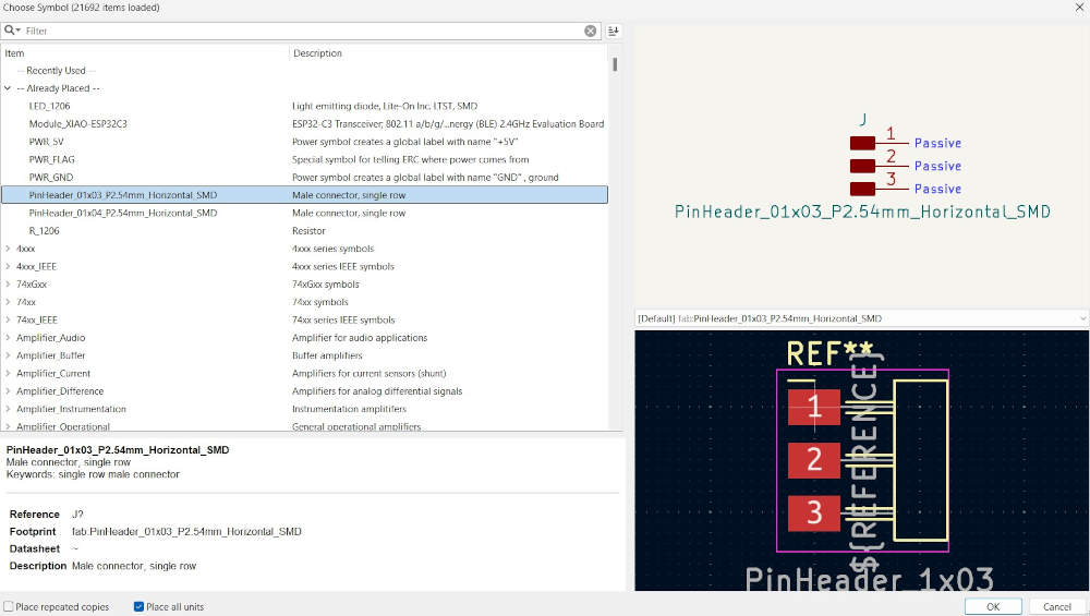
connect the pins with data etiquete.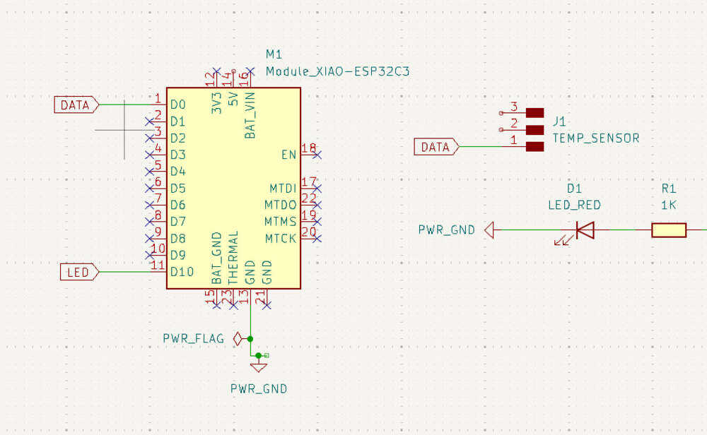
connect 5V and ground is very important to see the pinout to connect his part.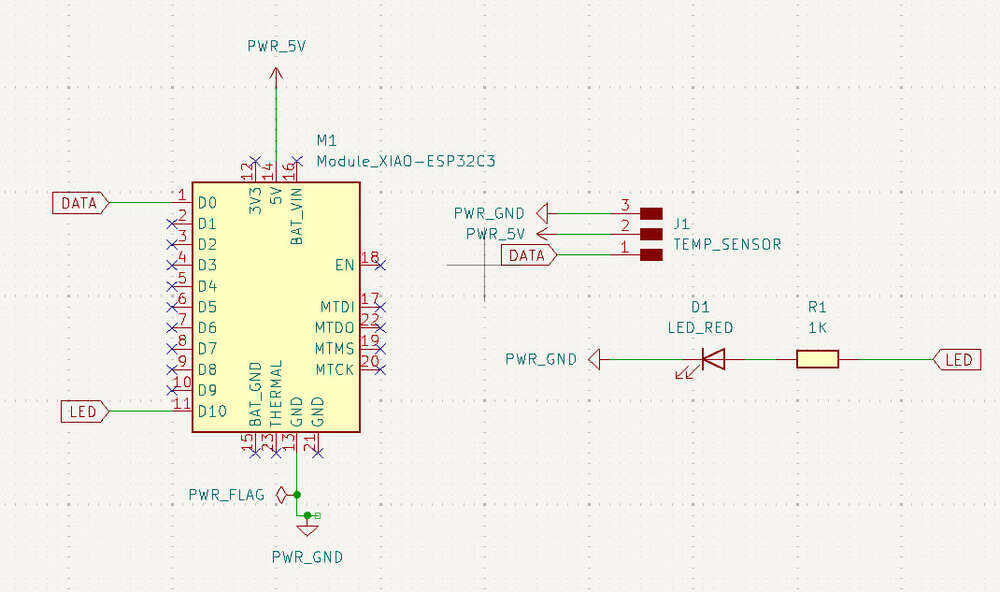
Connect the power flag so it doesnt show an error.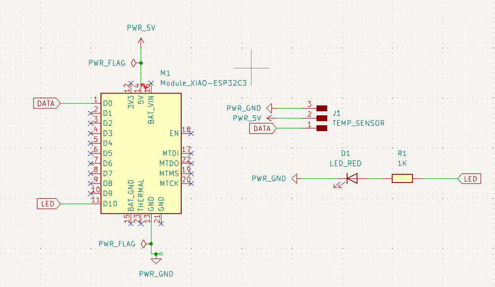
I add then a I2C communication and connect the corresponding pins.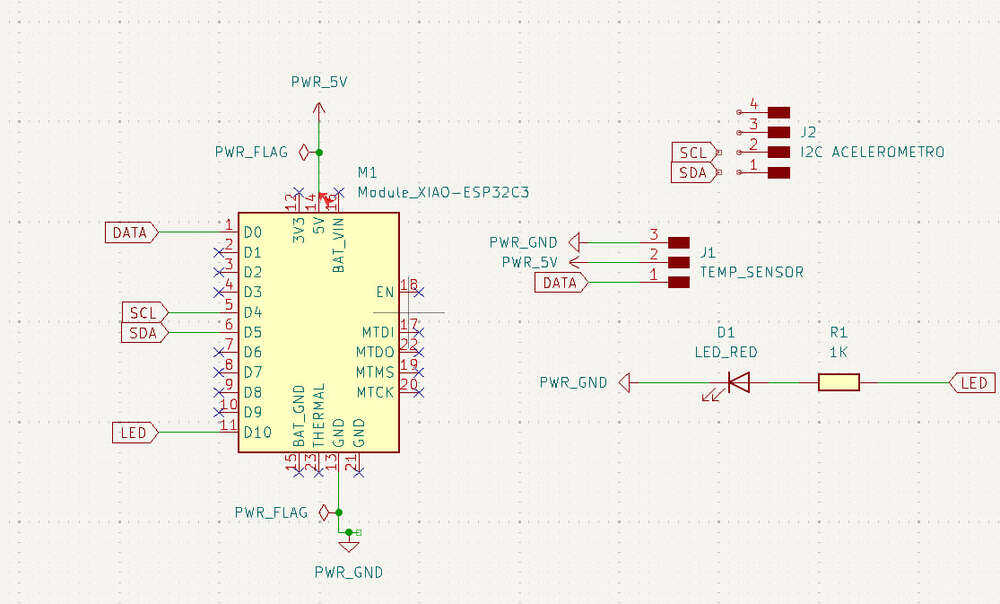
Adding the 5V and power ground pins.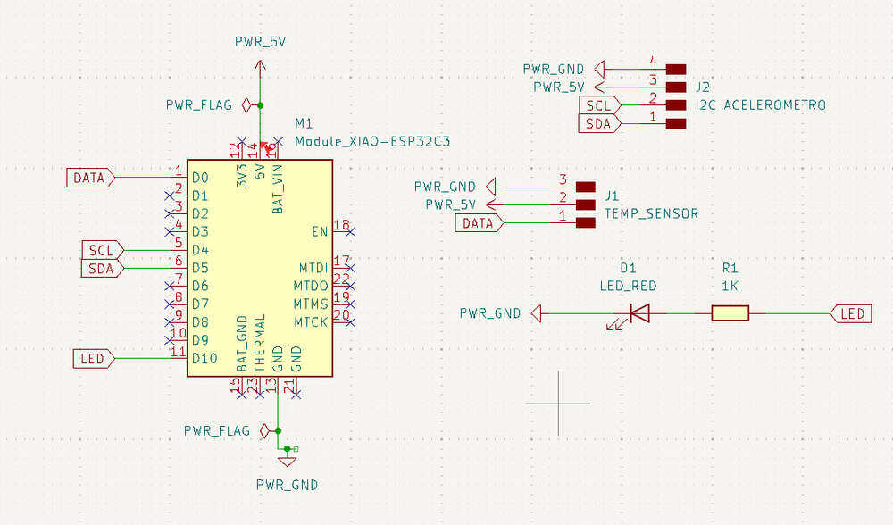
Then I went to the board edit to connect.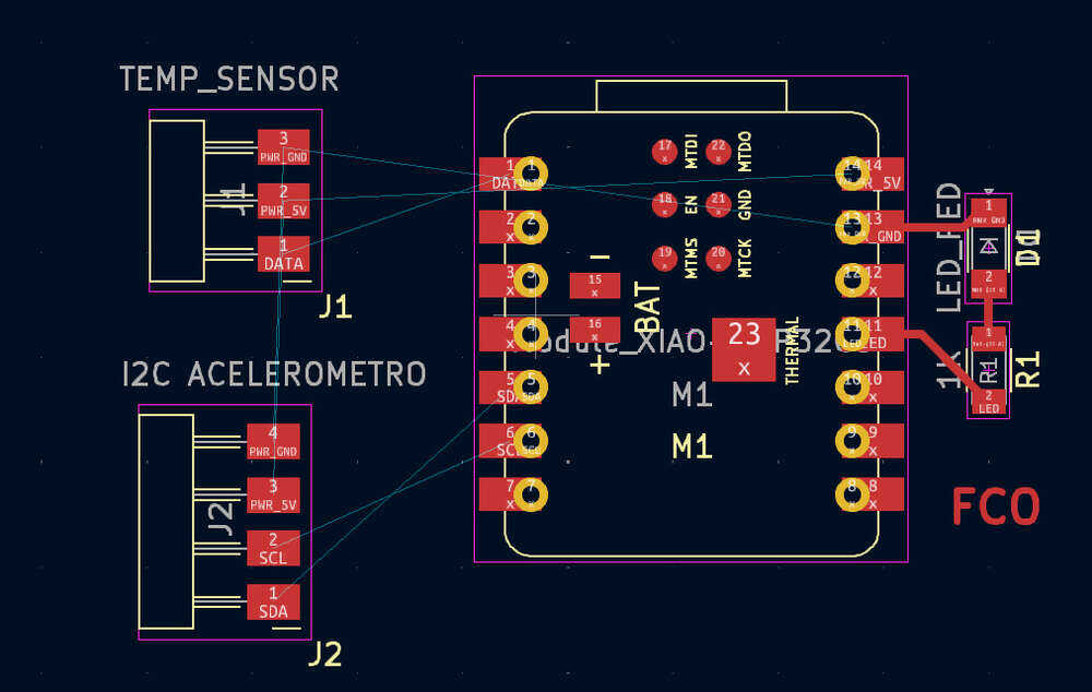
check error and warnings.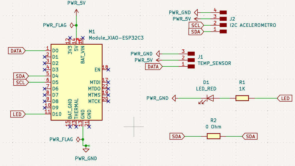
Very important tip, a resistor and be used as a bridge !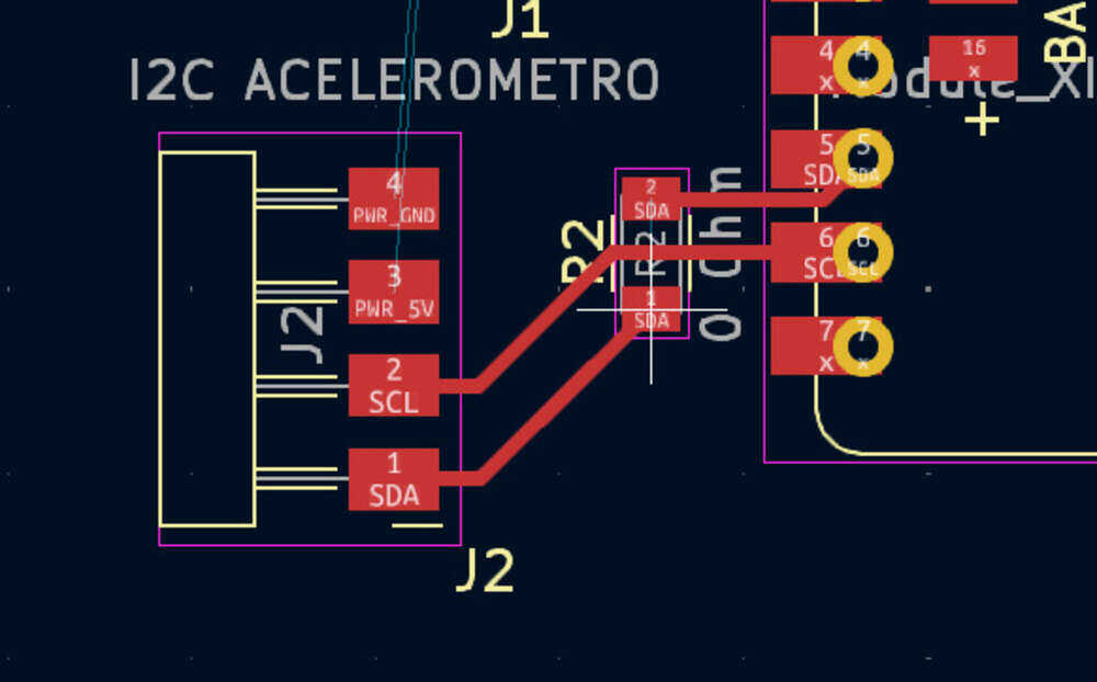
Other tip, use the board as a ground connector.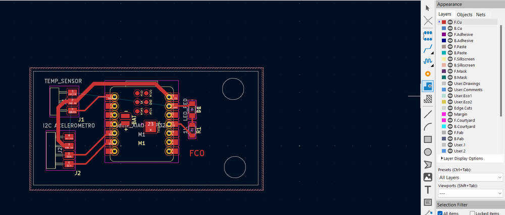
Fill al zones.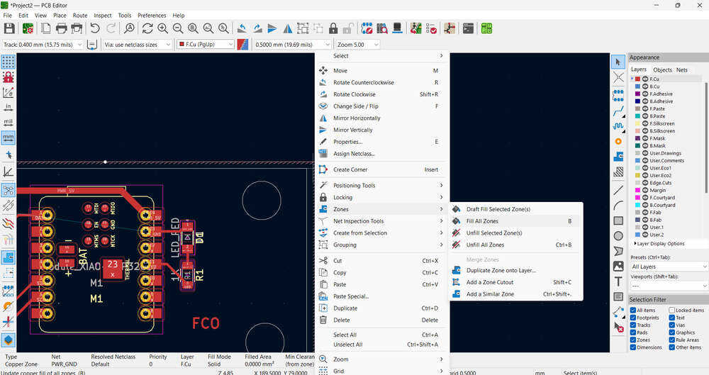
Board is ready for fabrication !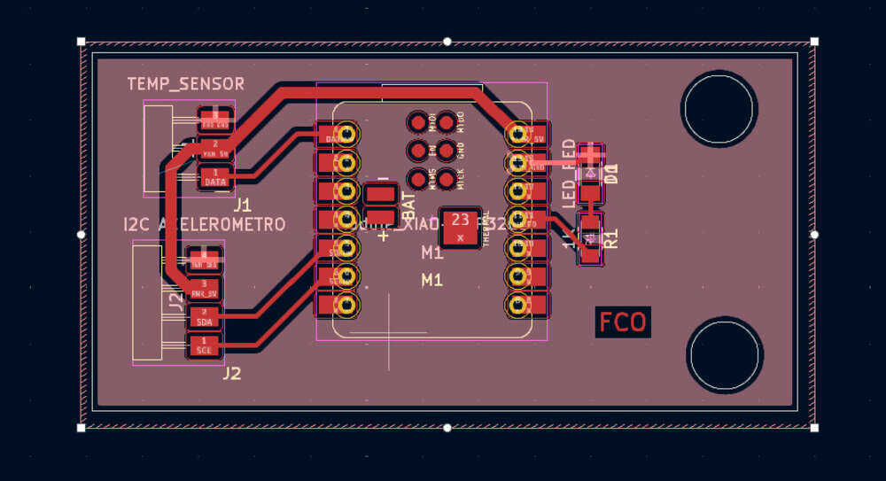
Interactive Html Bom is an extension that makes a list of item you have in the pcb.
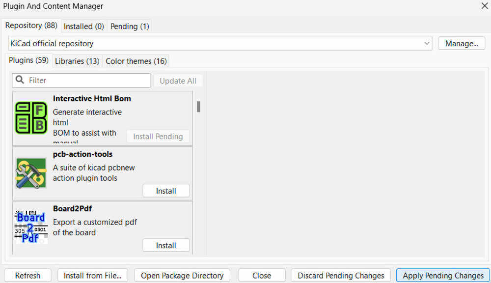


Learning Oucomes:
The learning outcomes of this assignment include understanding the fundamentals of PCB design using KiCad, learning to use lab instruments like oscilloscopes and multimeters for circuit analysis, and gaining hands-on experience in designing and troubleshooting microcontroller-based development boards. Students developed skills in schematic creation, component selection, and PCB layout, ensuring proper connections and error-free designs. Additionally, they learned best practices such as using resistors as bridges, optimizing power distribution, and preparing designs for fabrication. The assignment also reinforced the importance of documentation and iterative testing in the design process.
Documentation
- My first project: .zip click here
- Individual project: .zip click here