Week 8
Electronics Design
Organizing
checklist
| group assignments | — |
|---|---|
| Use the test equipment in your lab to observe the operation of a microcontroller circuit board (as a minimum, you should demonstrate the use of a multimeter and oscilloscope) | |
| Document your work on the group work page and reflect what you learned on your individual page |
| individual assignments | — |
|---|---|
| Use an EDA tool to design a development board to interact and communicate with an embedded microcontroller |
This will be my first time designing and making a breakout board PCB. I have followed a shot introduction workshop at my university not so long ago about the program KiCad from Casper who made really nice exercise on Github if you want to get started (in dutch). so I know a little bit about the workflow of the process but I have never designed a schematic of my own for a micro controller so this will be a challenge! I also have lots to learn about electronic components but I do have an understanding of the basic components like a resistor or capacitor.
1. Basic Electronic components
This week we got an introduction into electronics at Waag from Erwin I combined this information with Neils lecture about Electronics design and the book electronics for dummies that I started reading to understand the basics of electronics for the information below. It’s not documented in depth because I run out of time and there are so many information sources to get his knowledge so I just typed out some things I want to remember and really focussed on designing the skematic and board and documenting that.
Voltage: pressure the electrons are being pouched forwards Sum of the voltage in a loop should be 0
Current: the amount of electrons that are flowing (unit of measure in Amps)
Water analogy
The power (Watts) that both waterfalls can deliver are the same
one is high and long: small current high voltage
the other one is low and wide: big current low voltage
Electrons pushed in a direction: Direct current Electrons pushed in two directions: Alternating current
Most important formula: Power = V * I Power (watts)= V (volts) x I (amps)
Resistance Ohms law: R= V / I Resistance = volts / amps
- Wires, use them together if possible. EWG sets the diameter of the wire with charts that relate to the resistance of the wire.
- Bus: signals that belong together (for example 8 cables together).
Unpolarized vs polarized both direction voltage vs one direction
Components
Resistor
- no polarity
- current limiter, limiting the amount of water(current) that can go through
- SMD numbers the last number is the amount of 0’s to add to the value of the resistor
- resistor calculator
Capacitor
- storage for eclectic field charged over voltage
- used for filters, block some frequencies
- DC current open capacitor
- AC current acts as a resistor
- some capacitors have polarity (electrolytic) for direct current and you want to flatten the ripple
- its like a tank to store water
- symbol of two plates, plus size means polarized capacitor
- behavior of the ripple becomes like a weave instead of 90 degree angle because off the capacitor.
- with microcontrollers always put a capacitor next to it helps filter noise around it that is occurs because of the magnetic fields around the coper. Bypass capacitors Put between 5V ans GND 1uf (microfarad) capacitor
- huge capacitor can be useful as micro battery’s
Diode
- one way
- LED light emitting diode
- colors come from the material of building it
- turn it around it becomes light detecter
- capacitor can help the flickering of the LED
- full bridge rectifier
- forward voltage/current how much voltage/current you need as a minimum to light up the LED
Inductors
- storage for magnetic field in a relays or motor
- to switch huge amount of voltages and currents
- always use a diode (used the wrong way around) to prevent the magnetic field from flowing current back in to the circuit.
- it’s a variable transistor controlled by a gate.
Transistor
- bipolar transistor current (BJT), Mosfet transistor voltage (FET)
- can be used as an amplifier or switch huge currents like motor, speakers all kind of things.
- small signal to amplify
- you can connect to big things
- M Mosfet goes to ground
- P Mosfet goes to the power supply is a source of current
Regulators
- one side but a range of voltages
- 5 volts output input to 30 volts (regulator)
- can be inefficient DC - DC converters can be more efficient
2. Circuits
general principles
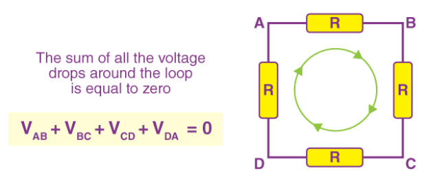
Kirchhoff’s law: current and voltage in and out within a circuit should add up to 0
- Resistors and diodes are used to make smart circuits
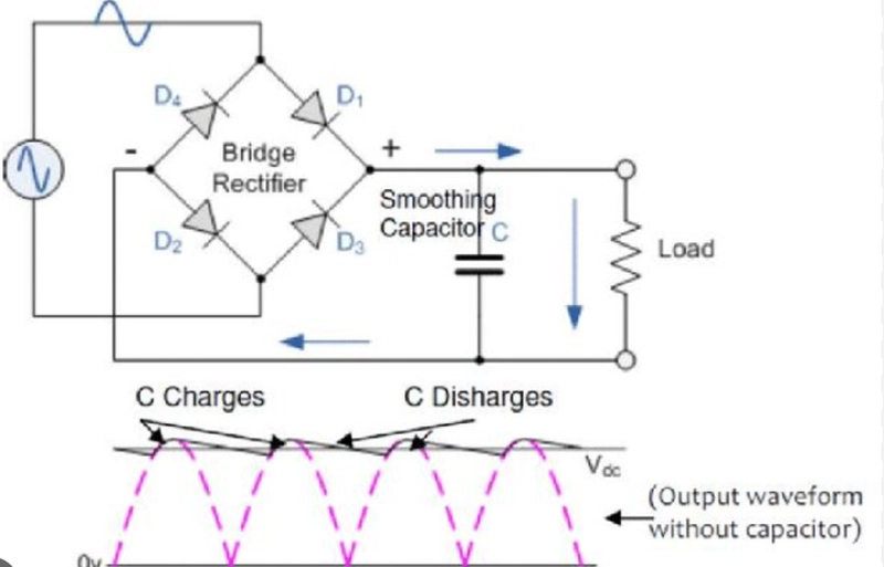
- bridge rectifier to convert AC input from main power to a DC output and to use smoothing the ripple when working on dimming a LED for example.
- H-bridge to make a motor move two directions.
- With analog components: Currents floating through in voltage drop use
- You might need to put heatsinks to help cool components with bigger powersuplies this will influence how lang for example a sensor lasts in a while
- be aware of power, measure power consumption in your devices
EDA Electronic design Automation, design tool for electronics I will use KiCAD If you use Fusion360. Eagle is a powerful EDA tool, integrated in Fusion
Virtual breadboard, Tinkercad, Fritzing all design online for simulate not for serious design work but fun for learning.
Sending a PCB to a board house
At Waag together we went through the process of sending a PCB to a board house fabricator I made screenshot’s of the process is class when I was working on a quick exercise of drawing a PCB.
For the design rules: look them up at the board house electronics fabricator you want to send your board to. Especially look for info about:
- hole size
- trace size
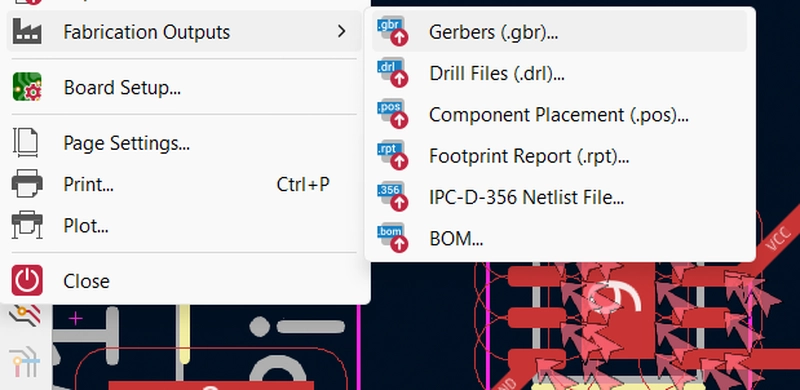
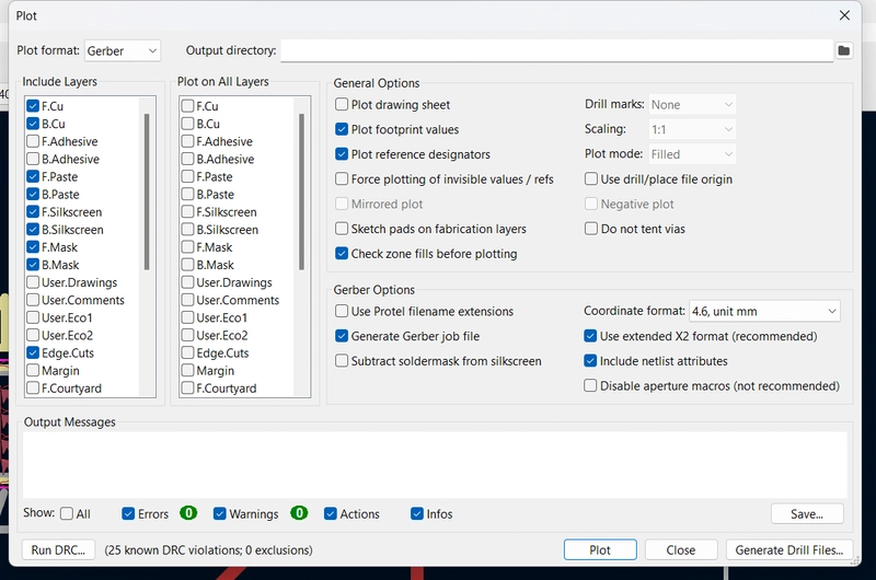
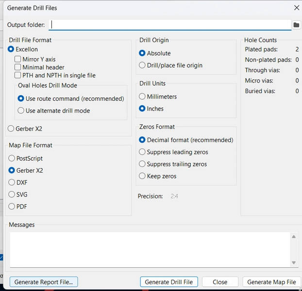
Export gerber files for sending it to a board house
Debugging electronics
Multimeter
To measure:
- voltage
- current
- resistance
- and much more
 COM - black minus cable
One for measuring voltages
One for measuring currents
COM - black minus cable
One for measuring voltages
One for measuring currents
I used the multimeter to measure resistance off charcoal for my final project conductive paint here and I used it to test my PCB if all the pins were properly connected in the continuity check stand in the picture below:
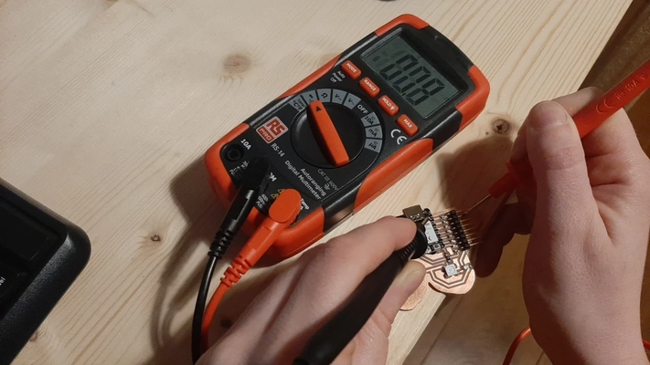
All the pins are connected!
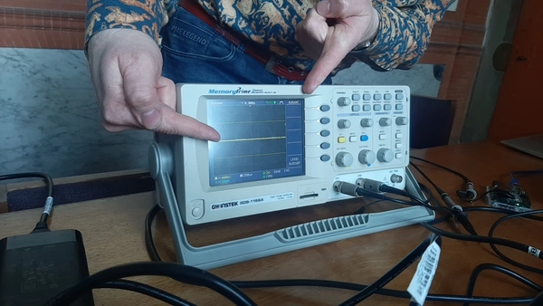
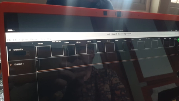
Oscilloscope
Measuring equipment for looking a longer period of time to the ripple of the voltage or current, you can see analog signals in wavy ripples. Edwin programmed an arduino uno and we used the oscilloscope to see what activity are going on on the pins. I didn’t document this properly when Edwin was demonstrating but I like michelle’s documentation of this machine. I do know what I can do with the machine and hope to use it for debugging in the future myself because I already forgot a lot about it.
- There are two kinds: Hardware based and PC based. At Waag we used a hardware based.
- The three most important buttons are the three big round buttons on the bottom side here you can change voltage and time.
- Two colors so you can hook up two channels and looks at the relation between the two channels.
- You can change the period of time by rotating the big button below on the right side to get a clearer view. You can also change the position of the ripple on the screen
- look at the screen to see the time in milliseconds and the Hz frequency of one block on the screen and calculate the length of a signal by counting blocks.
- You can measure analog signals
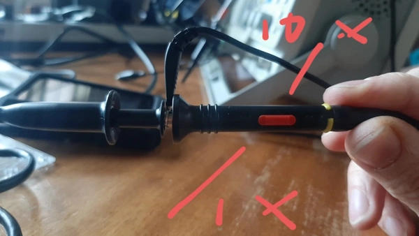
Yellow button is first cable ripple
Blue button is second cable ripple
There is a button on the probe to amplify the signal by 10x check if it’s 1x or 10x
Logic analyzer
Measuring equipment for digital signals only 1 or 0. high - low -Detailed signal
- Every cable has its own input
Individual assignment KiCAD
General knowledge and design steps to design my first PCB board:
- Install Fab academy library
- Design schematic for breakout board
- Assign the right symbols
- Create PCB
- Export PCB for CNC milling
- Mill and solder PCB
| KiCAD Shortcuts | – |
|---|---|
| A | In schematic editor adding components |
| V | change values (description) of the components for example change the value of the resistor to 499 Ohm (for your own documentation) for power you can use 3.3V for example |
| G | In schematic editor move components and lines |
| D | In PCB editor drag components while wires stay connected |
F.Cu (front coper) B.Cu (back copper) Past mask for reflow soldering Use black and white for export for Mods
Design Tips
- Snap EDA plugin for more component footprints and 3D files or download from their website.
- Route Single track default size track 0.2 mm width of the track/trace. This if for the board house.
- Milling your own PCB’s than it’s good to use 0.4 mm for connections of pins and 0.8 for connections of power.
- Cable connectors, move it back so the solder won’t handle the force.
- Try to avoid non rechargeable battery’s.
- Via’s go between top and bottom.
- 0 Ohm resistors can act as bridges in your design.
- Do a designrule check and a electrical rule check.
Today I start by having a hard time choosing to make a microcontroller chip to work with this week. I have the following options in my head:
- ESP WROOM
- ESP32 C3
- ESP32 S3 Sense
I joined the local review to get some more knowledge about how to start and what to choose. But I still haven’t made up my mind. At this time I think I might be able to design two boards one with the ESP WROOM for my input pillow and one with the ESP32C3 (since it’s cheaper) to design the output light. I start with the second one because it will be easier and also output devices is next week so seems logical. Because the ESP32C3 is cheaper than the ESP32 S3 Sense and I don’t want to use a camera yet, which i’m sort of obligated to when working with this super chip, since I have no clue how I choose the ESP32C3.
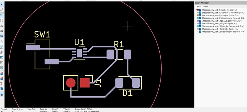
The schematic
tips
Use labels or wires
If you have multiple microcontrollers and sheets then labels. As a beginner use the wires
You don’t have to add wires all the time you can also add GND and VCC’s with the add global labels all the components need a unique name kiCAD does it for you
For making our own PCB’s we often use component size SMD (surface mounted device ) 1206 these are small but big enough to solder by hands.
for the pinheaders we often use 2.54 mm
don’t forget to do a Electrical Design rule check
I start with downloading the fabacademy KiCad library with al the components from the fab academy I download it here and have some troubles setting it up because I didn’t read properly.
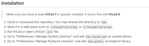 so don’t skip step 3 like me and try to import the libraries inside the schematic editor cause this wont work. I closed KiCAD opened it again and did it the proper way and I can now add footprints from the fab library. First step accomplished.
I continue reading about the chip I choose so the getting started on the XiaoESP32C3 here is very helpful as well as the sample board design Faxiao of Adrian here I decide I want to make a similar board to the Fabxiao. It will be a simple breakout board with a button a LED and with input and output pins digital and analog.! I read a bit about pins that already have certain uses that can glitch when setting up on the SEEED’s wiki page of this chip :
: D6 is set as a UART output at startup, so if you use D6 as an input, you may accidentally generate a high current. So it is recommended to use the D6 pin only in output mode.
However, since this D6 is a UART output, you have to be careful about a few things: one is that it is HIGH in standby mode when not communicating. The other is the text output of the 1st/2nd stage bootloader. The signal flaps HIGH/LOW immediately after start-up and must be counteracted if necessary.
So try not to use D6. (It’s okay to use it after you understand it, of course.)
So I think maybe then don’t connect it for a GIO purpose?
The text above confuses me because I have the button connected to pin D6 but Leo helps me clarify later on the mattermost chat that: pin D6 as you mention might have some startup stuff happening. You’ve got it connected to a switch and a resistor. No worries. They’ll survive. If this would be a highly sensitive sensor instead, then yeah, maybe don’t use this pin. So nothing to worry about, at this moment I was already finished with the design but I’m glad I now understand.
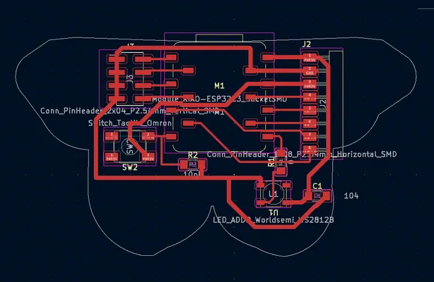
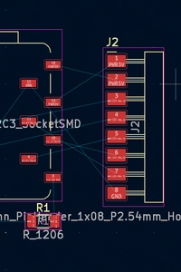
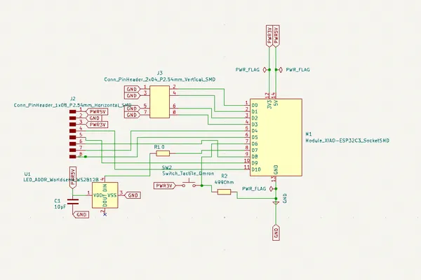
I start designing my PCB board using the program Kicad. Create a new project file and open the schematic editor I start with clicking on the button A this adds new components to my design. I start with selecting my micro controller and for this design I use the ESP 32-C3 I choose to add the footprint on pin-headers to I can later remove the chip and put it on another board design since I think I will have to make many more designs. I insert the component in to my schematic. I now select the the general unassigned resistor size 1206 by typing the letter R I add more components: pin headers, LED, tactile switch, power and ground.
After I edited all the components to the schematic I start drawing wires to connect the components to the microcontroller. I start with connecting the LED to pin number D7, the wire starts from the pin then goes to one part of the resistor then goes to the LED and then leave the LED via the ground wire. I then add the switch, I draw a line from pin D6 towards one end of the switch and draw the second end towards the ground. I also add a pull-up resistor between between the pin D6 and the ground. Later in the process I change these things because the switch should be connected to the V3 and the LED I change for a NEOpixel LED.
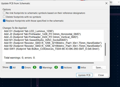
In the schematic editor I check if the design rules are correct by clicking on the electrical rules checker button. I first have some errors reporting it’s missing directions for the power and ground. I’be looked at Michelle’s documentation and see how she has fixed it with adding power flages. So I do the same. have no more errors and select the tool tab from the menu and I click on update PCB from schematic. The PCB editor pops up and it can recognize all the footprints so I press on Update PCB and click in the middle of my screen.
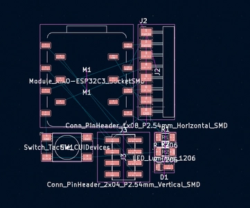
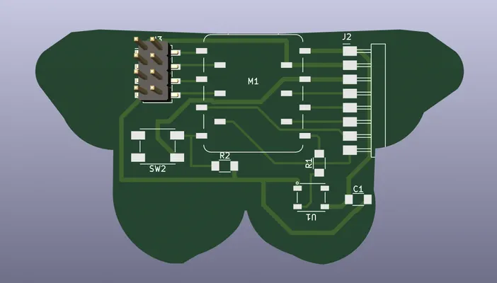
PCB Editor
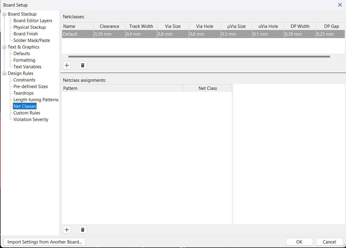
I now see all the components and I’m going to drag them and connect them with wires. The blue lines help me organizing the components put the analog pins on the left side of the microcontroller and put the switch and LED near to the connected pins. I conclude that I the gpio pins are organized messy. So I go back to my schematic editor. I change the order of the 5V 3V and the ground also the pins. I again click on update PCB from schematic I go to the PCB editor and select update PCB. Much better. I start with the puzzle to get everything connected and them remember that I first have to get the right board settings so i delete my wires and go back to michelle’s documentation. I go to file -> board set up and change the following things:
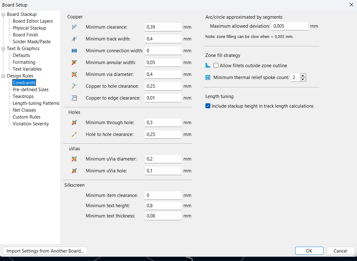
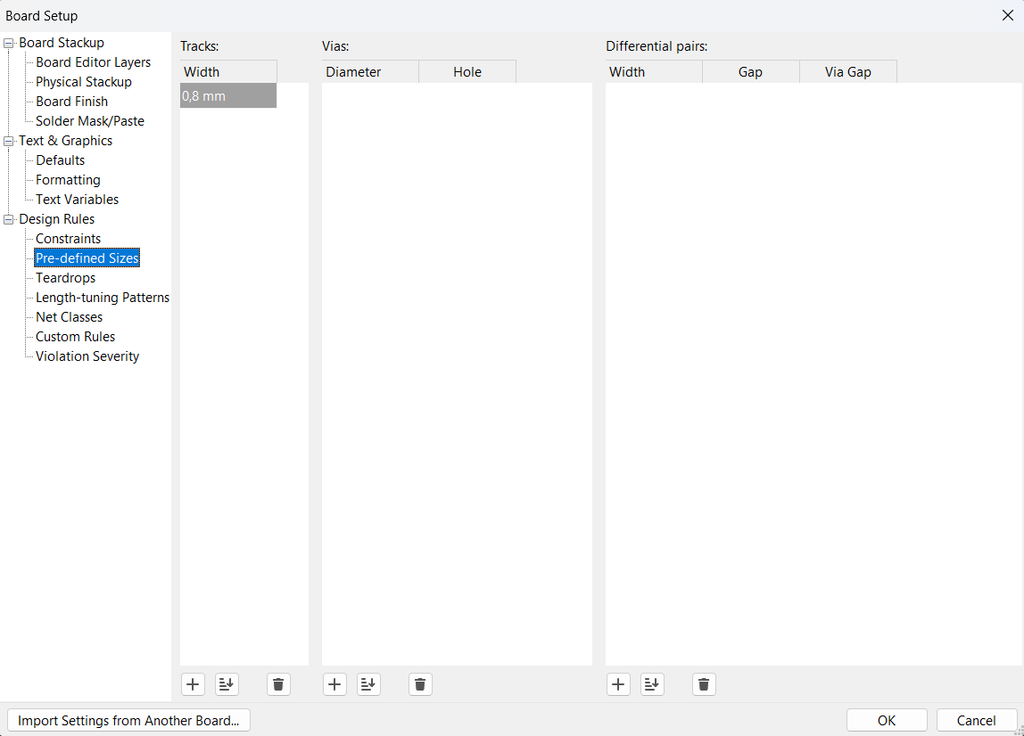
From the local review I heard it’s best to use 0.4 to connect pins and 0.8 for tracks that are connected to power. I select the tab underneath constraints called predefined sizes and add a new width in the tracks menu. I type 0.8 millimeters and press OK. I start with dragging power wires with 0.8 track width.
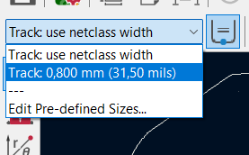 I now can shift between 0.8 mm size width and 0.4 in this menu. I connect the wires by selecting this symbol:
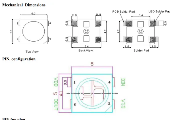
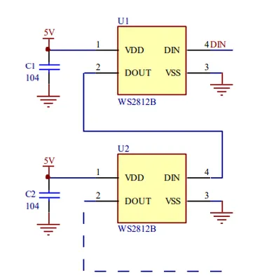
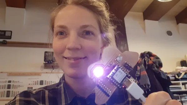
I connect everything and then decide to change the LED for a RGB LED Adafruit Neopixel because I want to add something on my own and I want to use these pixels in my final project so it seems like a good exercise. For this I look up the datasheet of the WS18B2 NEOpixel and look at the footprint and the schematic example. Showing me how to connect the component.
 I draw the new lines and when updating the PCB again I had to add a 0 Ohm resistor to make a bridge because otherwise I have to redesign the board again and I don’t want to to that.
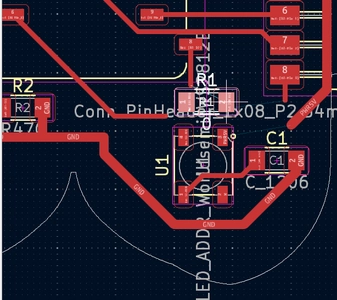
I also change the footprint of the button to the fab:Button_Omron_B3SN_6.0x6.0mm since I double checked my schematic next to Ardians FabXiao sample I noticed I had a different footprint and a different switch. For now I want to keep the switch the same. I also notice that I wired the switch different than Adrian. My switch went from ground to pin out between pin out and ground there was another resistor tp pull the floating pin down to GND. I don’t understand why Adrian’s button is connected to the 3V at first. It’s because I thought that pin’s always deliver an output current but they only do this when the pin is assigned to output state, and the button pin will be a Input so it can detect when the button is pressed. I spend a lot of time before I understand this but i’m glad I first try to design the board myself and then compare it because now I will not make this mistake again. The other confusion thing for me is that Ardian states he designed a PULL-UP button. And I don’t understand why it’s not a pull-down
What’s very important to understand is that the ESP32C3 and a lot of other boards have internal pull-up/pull-down resistors meaning in the chip there’s already these resistors. You can use them if you declare that you want to use them in your code.
So for example if you want to use the internal pull-up for the GPIO you type:
pinMode(2,INPUT_PULLUP);- This prevents the floating pin. In the case of Ardian’s example and also my own board we added a resistor on the board next to the button. So we won’t use the interna pull-up and type this in our code:
pinMode(2,INPUT); This clarifies a lot for me so maybe also for other people. For my board I decide to stick with the resistor on the board for now because i have it already there but in the future I want to design the board using the internal pull-ups / downs to help save space on the board. I fixed the doubts related to the switch together with Henk, Niels and Ardian thank you guys! And I informed myself with the following links:
https://magazijnrobotprojecten.jouwweb.nl/pull-up-pull-down-weerstanden
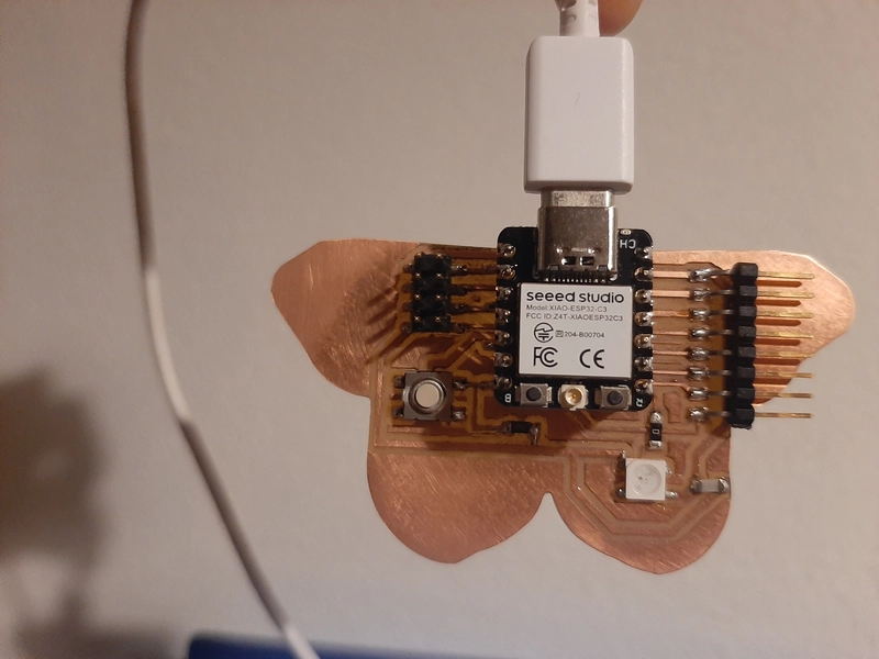
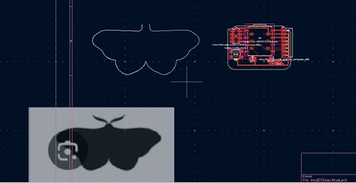
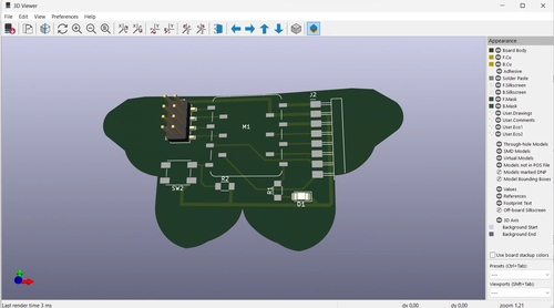
For the outershape I designed a butterfly shape I use a reference image from google that I import to draw the outline traces with the draw tools in KiCAD. I use the copy and mirror function to make them a big more symmetrical and make sure all he lines close. I use the 3D viewer to check this. If it’s not closed you wont see the shape here. I double check everything and I think I’m ready for the milling.
Milling the breakout board
At Waag I will use the Lunyee CNC 3018 together with Mods to mill my traces. I start by making a lot of exports, took my a while to get the export right. You have a lot of things to alter in the menu. What works best for me is using these export settings:
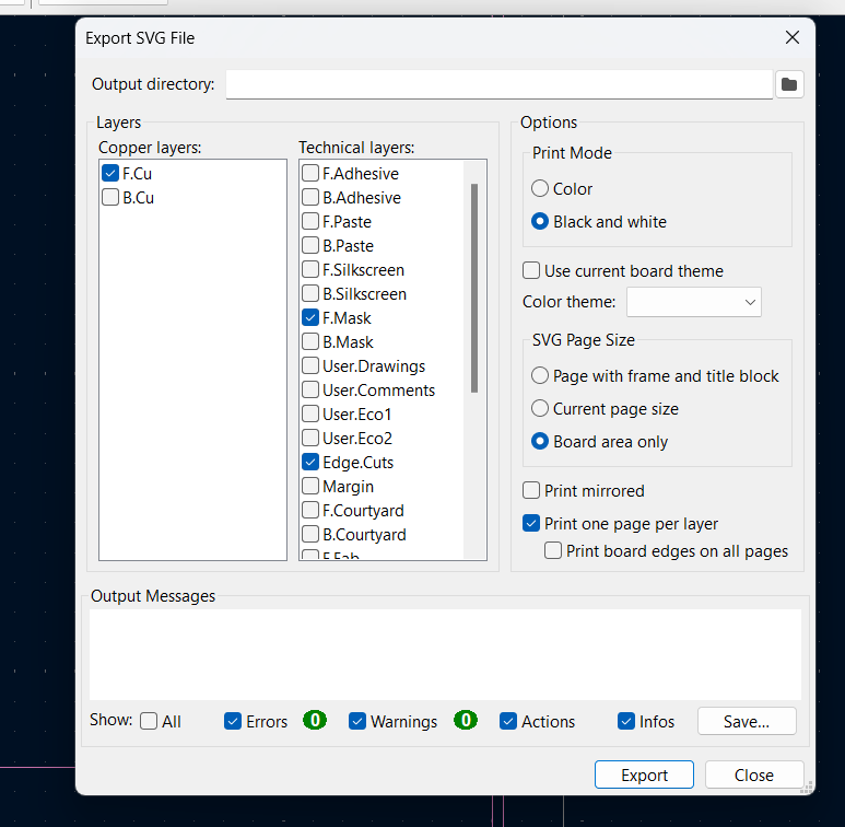
Since I’m only using one side of the PCB the front I only export the F.Cu (front coper) layer. For the technical layers I export the Edge cut in my butterfly shape and I export the Front mask layer because I want to try to make a reflow soldering mask, it export’s only the pads that I need to solder later.
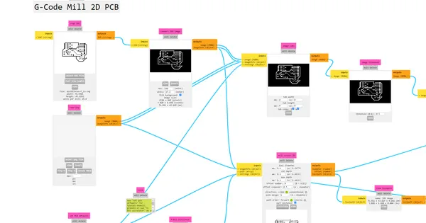
I look at my own documentation about mods and use this to make the traces. I have troubles inverting the PCB.
I did’t work with this last time but when I choose invert and calculate the traces again it just keeps milling the tracks instead of the contours around the tracks. I ask Henk to help me and together we are confused why it’s not working. After a while we decide it might be easier to invert the image in CorelDraw or Illustrator. I start with CorelDraw. 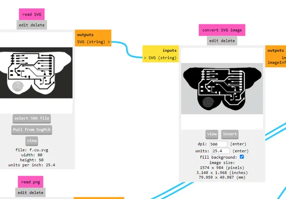 This is giving problems because it automatically opens a A4 size backdrop but I don’t want to save the SVG on this canvas size. And since my edge cut it in a different file I don’t like the workflow om creating a new backdrop and centring it. So I try Illustrator and design a backdrop but I notice from exporting the dimensions changed.
 We talked about this problem once and I look it up in Michelle’s documentation and here I found a reference to a video about inverting SVG’s in mods. I decide to focus on this instead because I like quick workflow for the future. I found out is the video that he presses a button called mill traces before calculating the settings in the mill raster 2C tab. Mods looks a bit different now but I can find the button underneath the set PCB default tab. I press this button, calculate and the invert finally works!
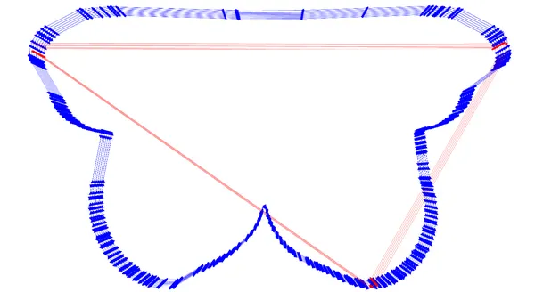
 So I try the same for the outline cut but I have the trouble it’s not a surface but a line and it’s inverting this line. Because the line is thinner then the tool diameter it’s showing no traces.
Henk helps me out and tricks the tip diameter of the tool to be 0.07mm so it will be able to mill to see and mill the outer cut line.
So I try the same for the outline cut but I have the trouble it’s not a surface but a line and it’s inverting this line. Because the line is thinner then the tool diameter it’s showing no traces.
Henk helps me out and tricks the tip diameter of the tool to be 0.07mm so it will be able to mill to see and mill the outer cut line.
 This works and I’m able to export a g-code. I use UGS for sending the g-code to the milling machine after leveling it here you find the documentation about working with the machine.
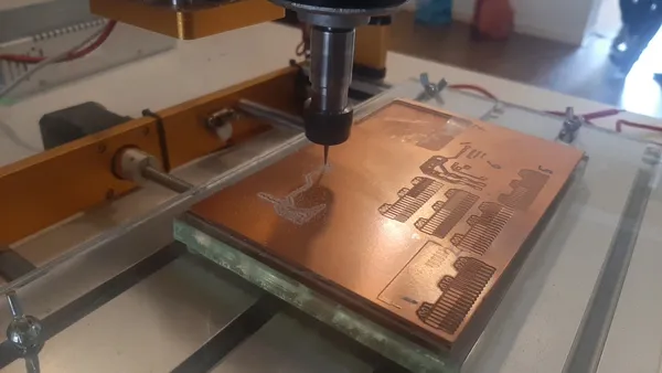 The traces needed an extra -0.1 mm after leveling with the paper method because it was etching instead of milling again
The edge cut had a weird order but everything looks good.
The traces needed an extra -0.1 mm after leveling with the paper method because it was etching instead of milling again
The edge cut had a weird order but everything looks good.
I need to deburr a little bit using the sponge and start working on the solder mask. For this I use DURA-LAR material I get from Henk to test if it work nice. It made of polyester and it’s a thin sheet. I cut out the traces similar to the edge cuts but then less deep, I cut it in two rounds the result had quit a lot of burrs and the pads are to big. 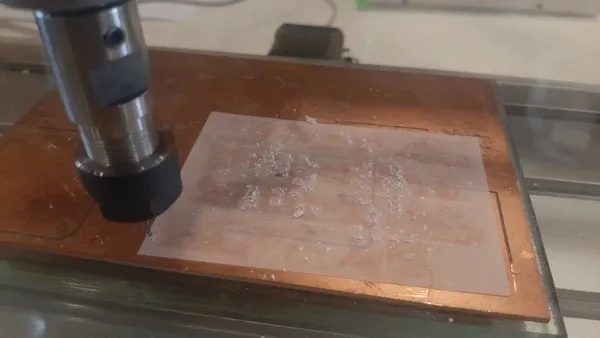 I have no time anymore to do a second try so for now I decide to hand solder the component. For the microcontroller I learned my lesson and first but the pin headers in before I solder them. Because I designed the board I know where the components need to go and I use the schematic to be extra sure. For the Neopixel I look in the datasheet and see one side has a triangle in the corner now I know how to solder the component.
Testing programming
I start the programming process by trying to get my NeoPixel to work on my breakout board. I follow Adrian’s steps on how to start programming the ESP32C3 on the Fabxiao board I make a few mistakes:
- accidentally selected the wrong board (clicked one higher)
- wanting to use the internal RGB LED but this in not so easy to use as with the RP2040 so I end up googeling a lot about the subject with Henk
- used the wrong pin numbers for Arduino programming with the ESP32C3 you need to use the D pin numbers and not the GPIO pin numbers as with the RP2040
- trying to many things at the same time to fix the problem
After redoing everything and selecting the right board and pin number the led starts shinning funky colors! I’m very happy I made the NeoPixel work!
 I used the following code:
//Fab Academy 2023 - Fab Lab León
//RGB LED
//Fab-Xiao
//original code from https://wiki.seeedstudio.com/XIAO-RP2040-with-Arduino/#rgb-led


#include <Adafruit_NeoPixel.h>

int PIN  = D7;
#define NUMPIXELS 1

Adafruit_NeoPixel pixels(NUMPIXELS, PIN, NEO_GRB + NEO_KHZ800);

void setup() {
  pixels.begin();

}

void loop() {
  pixels.clear();
  pixels.setPixelColor(0, pixels.Color(0, 0, 255));
  delay(4000);
  pixels.show();
  pixels.clear();
  pixels.setPixelColor(0, pixels.Color(0, 255, 0));
  delay(4000);
  pixels.show();
  pixels.clear();
  pixels.setPixelColor(0, pixels.Color(83, 83, 83));
  delay(4000);
  pixels.show();


}
I also test the button with the following code I made this code combining previous codes from the embedded programming week and Adrians examples.
#include <Adafruit_NeoPixel.h>

const int buttonPin = D6;  // button pin ESP32-C3 pin D6
int buttonState = 0;       // initial state of the button
int PIN = D7;              // LED pin ESP32-C3 pin D7
#define NUMPIXELS 1

Adafruit_NeoPixel pixels(NUMPIXELS, PIN, NEO_GRB + NEO_KHZ800);

void setup() {
  pinMode(PIN, OUTPUT);
  pinMode(buttonPin, INPUT);
  pixels.begin();
}

void loop() {
  buttonState = digitalRead(buttonPin); // Read the state of the button

  if (buttonState == HIGH) { // if the button is pressed
    pixels.clear(); // clears the pixel color and turns off all the LED
    pixels.setPixelColor(0, pixels.Color(15, 25, 205)); // set pixel color to purple
    pixels.show();
  } else {
    pixels.clear();
    pixels.setPixelColor(0, pixels.Color(155, 25, 5)); // set pixel color to another color
    pixels.show();
  }
}
Design files
BOM:
- “Reference”,“Value”,“Datasheet”,“Footprint”,“Qty”,“DNP”
- “C1”,“10pF”,“https://www.yageo.com/upload/media/product/productsearch/datasheet/mlcc/UPY-GP_NP0_16V-to-50V_18.pdf","fab:C_1206","1",""
- “J2”,“Conn_PinHeader_1x08_P2.54mm_Horizontal_SMD”,"~”,“fab:PinHeader_1x08_P2.54mm_Horizontal_SMD”,“1”,""
- “J3”,“Conn_PinHeader_2x04_P2.54mm_Vertical_SMD”,“https://cdn.amphenol-icc.com/media/wysiwyg/files/drawing/95278.pdf","fab:PinHeader_2x04_P2.54mm_Vertical_SMD","1",""
- “M1”,“Module_XIAO-ESP32C3_SocketSMD”,“https://wiki.seeedstudio.com/XIAO_ESP32C3_Getting_Started/","fab:SeeedStudio_XIAO_SocketSMD","1",""
- “R1”,“0”,"~”,“fab:R_1206”,“1”,”"
- “R2”,“499Ohm”,"~",“fab:R_1206”,“1”,""
- “SW2”,“Switch_Tactile_Omron”,“https://omronfs.omron.com/en_US/ecb/products/pdf/en-b3sn.pdf","fab:Button_Omron_B3SN_6.0x6.0mm","1",""
- “U1”,“LED_ADDR_Worldsemi_WS2812B”,“http://cdn.sparkfun.com/datasheets/BreakoutBoards/WS2812B.pdf","fab:LED_ADDR_Worldsemi_WS2812B","1",""
- here you can download the KiCad file
- here you can download the g-codes fot the milling, Enge cut, traces and mask.
Reflection
This week went well, I took a lot of time double checking everything because I wanted to be sure I fixed my mistakes before I put in the effort of milling and soldering. Which worked out well! With the programming I should have been more rested and awake, I did it at the end of a long day I just wanted it to work very badly! And then I made stupid little mistakes that took me much time. I’m glad I put in the Neopixel to make the design of the board more of my own. And to look at a datasheet for the orientation. I also spend quit some time trying to understanding why the button is connected the way it is and whats up with these pull-down and up resistors and capacitors, but I’m glad I did. I need to understand things at a certain level to be able to do more than just copping something. So I think it’s time well spend. I learned a lot!