Week 4
Electronics Production
Organizing
checklist
| group assignments | — |
|---|---|
| Characterize the design rules for your in-house PCB production process: document feeds, speeds, plunge rate, depth of cut (traces and outline) and tooling. | |
| we will do this during electronic design week | Document the workflow for sending a PCB to a board house |
| Document your work to the group work page and reflect on your individual page what you learned |
| individual assignments | — |
|---|---|
| Make and test a microcontroller development board |
PCB production with CNC
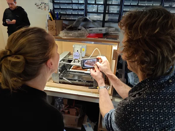
This week I did the group assignment together with Edwin. You can find his documentation here. We worked on the Modela and the 3018 and tested 3 different types of bits and various settings. You can read all about it on this page and Edwins page. I will first start with some general knowledge about working with a PCB milling machine and explain the two workflows of the machines.
materials
Types of plate material for PCB’s at Waag:
- FR 1 - paper based.
- FR 4 - fiberglass based.
- Double sided FR 1, paper based use rivets for going to the other side.
- Recyclable board, made of jute and water resolvable epoxy (hard to work on because the coper layer cracks easily).
We will use the paper based FR 1 material because we don’t want micro partials of fiberglass floating around in the air. So FR 4 is a no go when milling PCB’s.
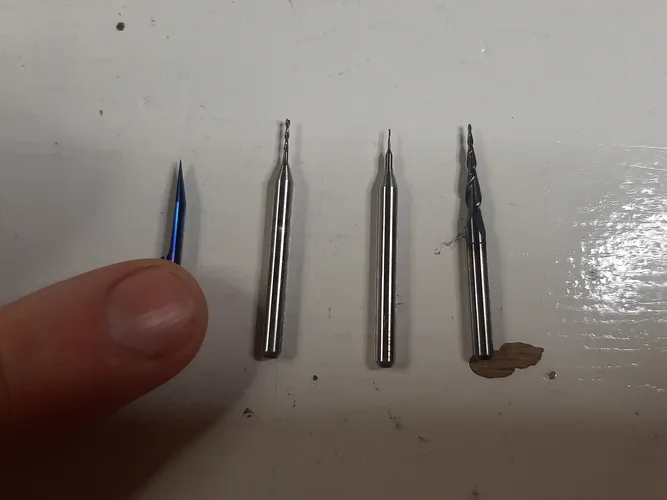
Types of bit’s:
| — | size in mm | angle in degrees | use | pros | cons |
|---|---|---|---|---|---|
| Tapered bit with a ball nose - on the right side of the picture | 0.25 | 15 | milling coper traces, milling FR1 and drilling | tough tool, can do everything with one bit | more trial and error to find the right settings because of the angled tapered bit and more burr |
| End mill - second from right | 0.4 | - | milling coper traces | the flat end drills away a neath thin layer and the edges are clean | Can be 20 times more expensive than a V bit, fragile cutting blades, can’t make extremely thin innercuts |
| End mill - second from left | 0.8 | - | milling FR1 and drilling | ||
| V bit- on the left side of the picture | 0.1 | 30 | traces, drilling and cutting | super cheap and a bit tougher then the end mills | more trial and error to find the right settings because of the angled bit, more burr |
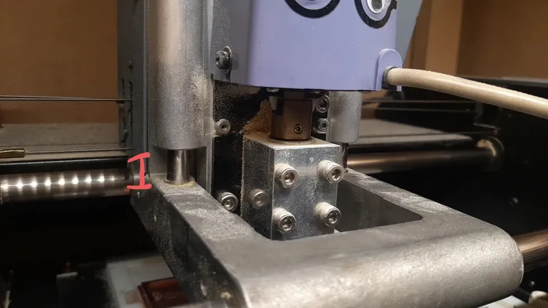
The machine working area has lots of layers I will start explaining them.
- machine bed the transparent layer is the bed of the machines
- level layer the white layer is the level layer made with the milling bit on the same machine so it’s always perfectly level.
- sacrificial layer the PCB that says do not cut it the sacrificial layer for when you cut out boards.
- PCB the PCB on top of that is the PCB to cut out. Use double sided tape to fasten the PCB but don’t overlay the tape instead place them neatly near each other.
Important Settings
Note: in mods use PCB default (for straight bits and tapered bits) and V-bit calculator (for v-bits).
- Cut depth: depth of one “layer” With end mills the depth is less than with angled bits. The average thickness of the coper layer is 35 microns in thickness (0.035 mm). You wan’t to cut away more then that.
- Max depth: when milling through the PCB plate for the outline or to drill holes you type the max thickness here.
- offset number: number of lines next to each other to create the clearance. When hand soldering the components it’s best to have 1 mm clearance. The tool diameter depends the amount of offset lines. With angled bits you typically need more lines then with (flat)end mill bits.
- offset stepover: took me a while to understand it, this is a unit so 0.5 means half. It’s the overlap between the offset lines. With the offset number we talked about the 1 mm clearance. If the tool diameter is 0.4 mm we would need 2,5 lines to get to 1 mm you would think, but this is incorrect because: the path’s need to overlap so no copper wil be left behind between the lines. So offset stepover 0.5 tells the machine it will overlap half of the tool diameter every line. So the first line is 0.4 in width the second is 0.4 but overlaps half so total width is 0.6mm, next one makes 0.8 and the 4th line gives us the 1 mm offset.
- feed speed: movement of the head in X, Y direction mm per seconds. (not the spindle)
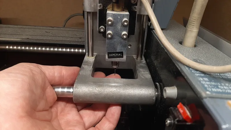
Getting Started with the Modela
The Modela is a small PCB machine made for milling PCB circuit boards.
Erwin shows us at Waag how to work with the machine.
Prepare machine
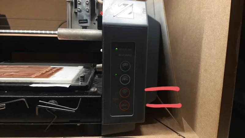
Machine buttons
- On: put the machine on
- View: lets you inspect the PCB by bringing the bed forwards, you can’t start the machine when it’s in view mode.
- Up: moves the head up, use this for changing tools.
- Down: moves the head down, use this for changing tools.
- Press up and down simultaneously to reset/clear the memory of the machine. The machine will blink until you take out the USB cable and plug it back in.
Prepare the machine
- Take out the board by unscrewing the two screws in front and use a putty knife to remove the old PCB.
- Clean the PCB with sicker removal (or oil - tip from Leo).
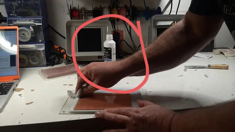
- Fix the PCB plate thoroughly because the axis moves in al the directions.
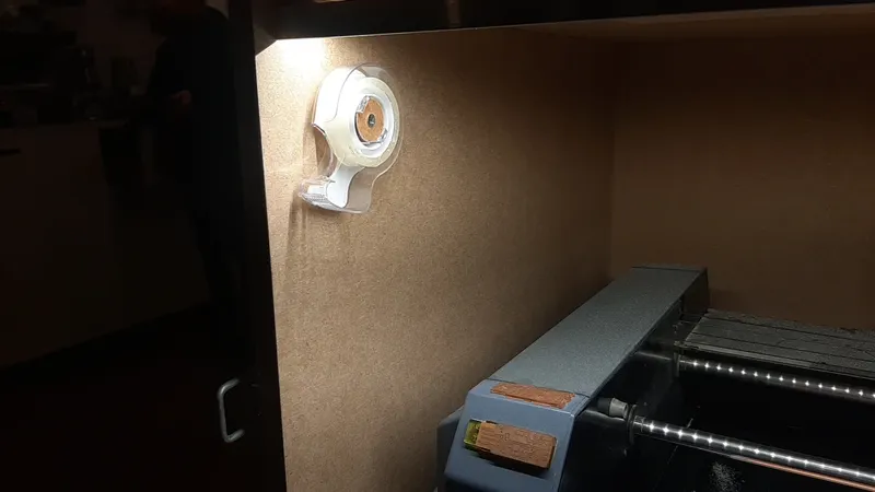
- You need enough tape and don’t overlap the tape because of the levelness. You can find the tape here:
- Tighten the screws again
- Look for the mill bit’s in the boxes and choose one.
Go to mods for this part, more about mods later, and move the head to create a new origin by changing the X and Y. The machine wil start in the lower left corner.
- Open the collet by loosening the small screw that does not have the black tape. Use the Up button if you need more space. But the bit inside the machine, a bit higher than you want it to be.
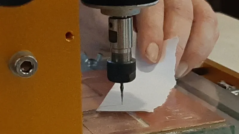
- Lower the head of the machine until the milling bit is about 1 mm above the PCB plate. Use the down button on the machine to do this(don’t do this in mods). The zero is set now set to this point. Watch out don’t lower it to much, the machine still needs to be able to go lower for the milling.
- Level the milling bit by loosening the screw, hold the bit in the other hand and gently let the tip touch the coper plate. The milling bit is now level!
- You can use the view button on the machine as a pause button when the machine is running.
- If the machine is finished it will returns to view mode. clean it with the vacuum:
Prepare mods
- Go to mods right click -> programs -> open program -> roland -> Modela MDX-> PCB
- Load the file in the read png menu on the left (make sure to chose the right one: traces, outline of the board and or drilling holes).
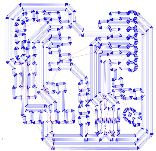
- Important: mods has two menus with default settings that, when altered, calculate the settings for the mill raster 2D Take a look at the default settings for set PCB, when using the end mill change this menu and click on the mill traces button for example when milling traces. If you use an angled bit take a look at the V-bit settings and change settings before hitting the send calculated settings it wil calculate the tool diameter based on the tip diameter and angle. Watch out for inches and millimeters and make sure you fill in the right boxes. You can also skip the present settings and fill in your numbers directly in the mill raster 2D menu is you know your numbers. You can find al my settings and test results in the menu’s on this page below.
- Go to the webSerial menu and select get device -> select the device -> usb serial controller
- Always recalculate at the mill raster 2D menu to be sure you have al the settings. And always write down the x y destination (origin) so you can go back to it when breaking a bit or closing mods for example.
- Inspect the traces and look if there is enough detail and cleaners at the view toolpath menu press View
- Send the file at the wright below corner. Watch out, the machine will start right away if it’s out of view mode.
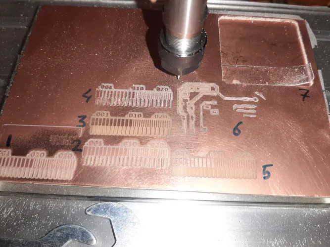
Tests
| Modela making traces | tool | tip diameter | cut depth | max depth (one pass) | tool angle | offset number | offset overstep | feed speed |
|---|---|---|---|---|---|---|---|---|
| test 1 | end bit | 0.4 mm | 0.07 | 0.07mm | non | 4 | 0.5 | 4 mm/s |
| test 2 | V-bit | 0.1 mm | 0.2mm | 0.2mm | 15 | 6 | 0.2 | 4 mm/s |
| test 3 | V-bit | 0.1 mm | 0.1mm | 0.1mm | 15 | 4 | 0.2 | 4 mm/s |
| test 4 | V-bit | 0.1 mm | 0.1 mm | 0.1mm | 30 | 6 | 0.5 | 4 mm/s |
| test 5 | Tapered ball nose | 0.25 mm | 0.1 mm | 0.1mm | 15 | 4 | 0.5 | 4 mm/s |
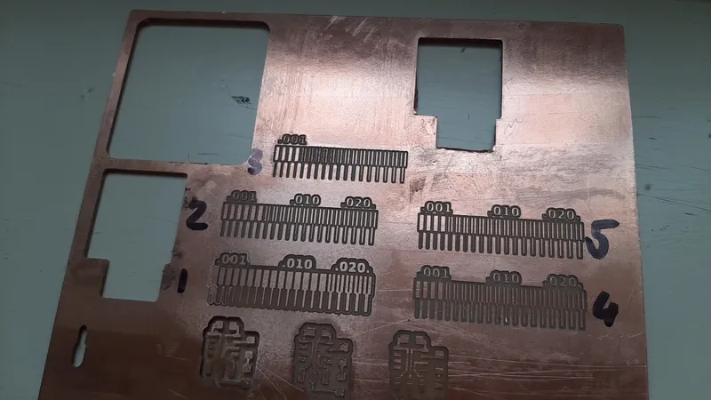
Test notes
- Test 1 : Cut depth looks good, the lines are clean no burr, the end bit of 0.4 mm is not able to make extremely thin stripes in the middle of the test sample.
- Test 2 : The lines are not connected, missing as the lower lines in the left corner. To much material is milled away and therefore we are missing traces. The preset settings changes offset overstep to 0.2 instead of o.5 Edwin and I think it’s (because of the V shape)
- Test 3 : Changed the cut depth form 0.2 to 0.1 mm to see if this fixes the problem from test 2, worse result
- Test 4 : Henk help us because we didn’t understand, turned out we had the angle wrong V-bit has an angle of 30 degrees and the tapered bit of 15. So we messed them up, and changes it. Also we put the offset overstep to 0.5 instead of the preset of 0.2 mm. The result is a bit better but not really, but it’s the best try for the V-bit. We decides to quickly test the tapered ball nose as the last test before we switch machines.
- Test 5 : result has less burrs but still the traces are not connected properly, however the innercut traces are milled very nicely! The other traces however are not jet perfectly connected so it still mills away a bit to much material. Henk gives the tip to pretend the bitt point is 0.3 mm instead of 0.25 mm so that the machine will etch away less at the outer edges, we will try this with the 3018 CNC.
Important things when working with the Modela
- Remember the origin when working with the Modela wright it down somewhere!
- don’t open a new mods while another is running, the mill will stay stuck at its drilling place and you need to reset the machine.
- When working with tapered / V bit’s the bit’s are able to make thinner traces. But I if you are going to solder we need 1 mm clearance between the coper traces and this takes a lot of time because the traces are way smaller than the end mill.
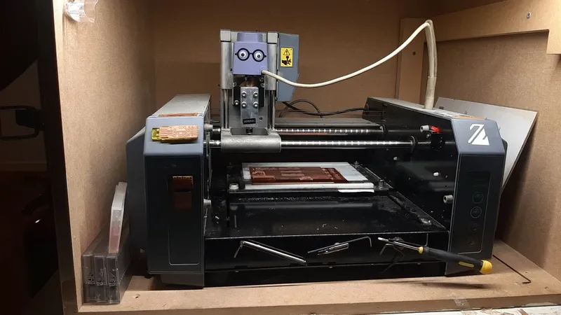
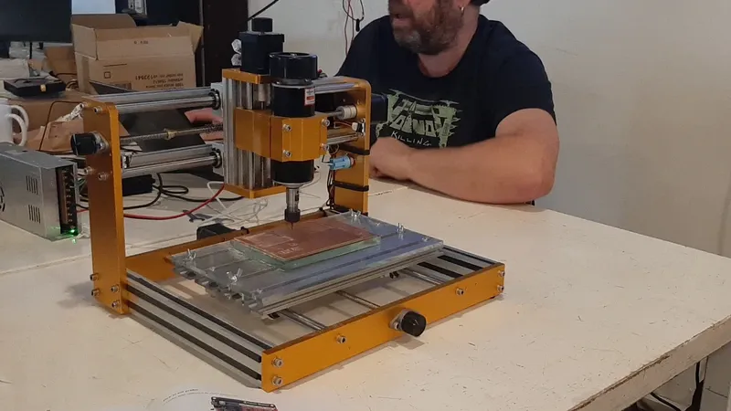
Getting started with the Lunyee CNC 3018
The Lunyee is a affordable CNC machine and Waag changed the Spindle for a better one that has 500 wat to have high end results on this machine. Henk shows us at Waag how to work with the machine.
Prepare in mods
Prepare mods the same as you did for the Modela but make sure you choose the right machine in the beginning. We will create the G-code in mods but we will start the machine from a different program named UGS (Universal Gcode Sende). Download the program here.
- Go to mods -> right click -> programs -> open program -> machines - G-Code - Mill 2D PCB
- Insert the right settings, I already gave an explanation about the most important setting on this page and of course you can look at my test results for the settings I used.
- hit calculate at the mill raster 2D menu in mods
- view toolpath to see if you have al the traces and enough clearance.
- The g-code should download automatically when you recalculate. If not put the switch on at the on/off menu in mods.
Prepare the machine with UGS
- Open UGS and plug in the usb cable of the CNC in your laptop.
- connect the device by clicking on the orange button in the menu. When the button is orange the device is connected. In this menu you also see the send button (right from the connect button) and the stop and pause button.

- Load the g-code file.
- go to the toolbox and switch tabs to jog controller on the left side of the screen
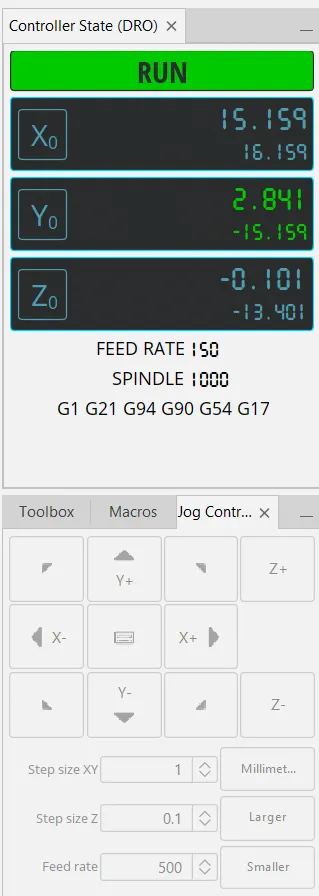
- You can change the step size and feed rate to your likings and move the spindle, this workflow is very nice because you don’t have to fill in numbers. You can just watch and adjust from your laptop by clicking the buttons in the jog controller.
- The machine will start from the bottom left again. Go to a a free spot on the F1 plate and make sure you measure if there is enough space for your design.
- If you click on the X0, Y0 and Z0 buttons underneath RUN the machine will set the current coordinates at a new origin (zero). Set a new zero for the X and Y axis.
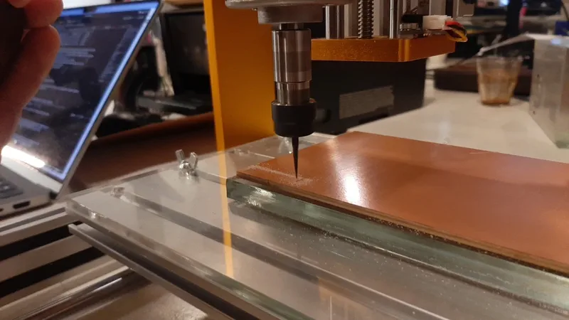
- open the collet using two wrenches and put in the right tool and fasten it again. Make sure it’s tight and straight for you safety!
- Now level the Z axis by using the paper method described below. make sure to hit the Z0 button after you leveled it to set the new zero.
- Send the file to the machine, with the start button next to the connection button, the machine will start right away!
Tests
| Lunyee CNC 3018 making traces | tool | tip diameter | cut depth | max depth one pass | tool angle | offset number | offset overstep | feed speed | notes |
|---|---|---|---|---|---|---|---|---|---|
| test 1 | Tapered ball nose | 0.30 mm (it’s actually 0.25) | 0.1 mm | 0.1 mm | 15 | 4 | 0.5 | 4 mm/s | bit number 1 |
| test 2 | Tapered ball nose | 0.30 mm (it’s actually 0.25) | 0.1 mm | 0.1 mm | 15 | 4 | 0.5 | 4 mm/s | bit number 1 offset -0.2 after removing the paper |
| test 3 | Tapered ball nose | 0.30 mm (it’s actually 0.25) | 0.1 mm | 0.1 mm | 15 | 4 | 0.5 | 4 mm/s | new bit number 2 |
| test 4 | Tapered ball nose | 0.30 mm (it’s actually 0.25) | 0.1 mm | 0.1 mm | 15 | 4 | 0.5 | 4 mm/s | bit number 1 |
Test notes
- Test 1 : First Tapered ball nose test, put the tool diameter at 0.30 instead of 0.25 because of the result on test 5 on the Modela. Used the paper leveling method. The result is better then Test 5 of the Modela (with the same bit). So Henk’s advice worked, but we have a weird leveling issue, where the bit is more etching then milling the coper away. We did an extra -0.05 mm on the Z axis. And the cut is a bit deep after that and needs some sanding with the fiber sponge.
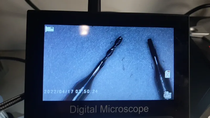
- Test 2 : We try it again with the same settings thinking we might have done something wrong while leveling. We have the same problem and need to go down even further (-0.2) after removing the paper. What is odd is that an the lines on the left side of one test block are etched and on the right side are milled. In can’t be a level problem because on the right left and in the middle of the board we have the same issues. Times up and we decide to call it a day. I think it might have something to do with the blades of the tool. But I can hardly see the blades on the microscope..
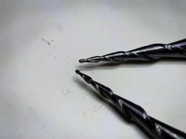
- Test 3 : Friday I test a different (new) tapered bit, same size same settings and leveled it with the paper method -0.1. The result is the best I had so far, no burrs, all the lines are connected. almost half of the thin innercuts are there and all the outerlines on the left look good. So I’m super happy about the result! To make sure my theory is right I do one more test with the old bit.
- Test 4 : Same bad results as test 1 and 2, so it’s very likely there is something wrong with the bit. I will use the newer bit and test 3 settings for working on my micro controller.
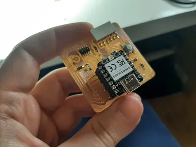
Making the microcontroller development board
I download the files for the Quentorres board designed by Ardián here, I will make a board for the XIAO RP2040 here you can find the getting started with it link.
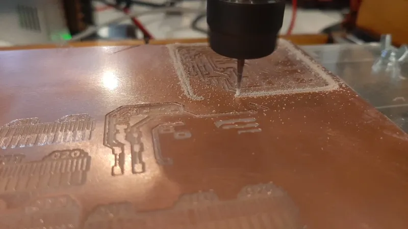
Milling
| Lunyee CNC 3018 | tool | tip diameter | cut depth | max depth (one pass) | tool angle | offset number | offset overstep | feed speed | level |
|---|---|---|---|---|---|---|---|---|---|
| milling traces | Tapered ball nose | 0.30 mm (it’s actually 0.25) | 0.1 mm | 0.1 mm | 15 | 4 | 0.5 | 4 mm/s | offset -0.1 mm when leveled on paper |
| Drilling holes | Tapered ball nose | 0.30 mm (it’s actually 0.25) | 0.23 mm | 1.6 mm | 15 | 1 | 1 | 4 mm/s | offset -0.1 mm when leveled on paper |
| Milling the outline | Tapered ball nose | 0.30 mm (it’s actually 0.25) | 0.23 mm | 1.6 mm | 15 | 1 | 1 | 4 mm/s | offset -0.1 mm when leveled on paper |
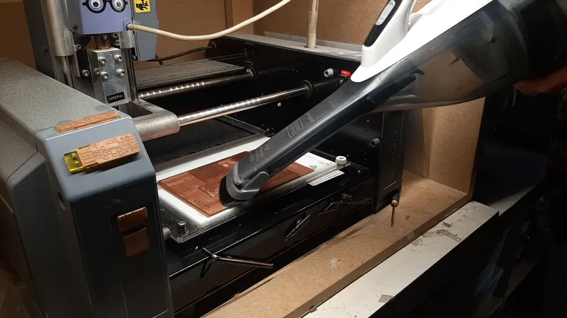
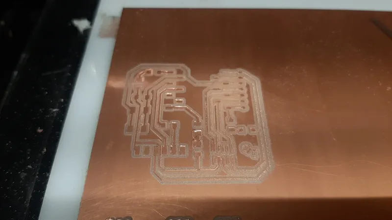 Milling traces: I level the new bit of Test 3 on the Lunyee CNC 3018 and start milling my micro controller for the first time. I see that the bit is cutting a bit more material than i would want it to be, so the paper level method is not as waterproof as I would want it to be. I have a bit more burrs but I leave it as it is. Strangely the CNC decides to get stuck in one spot and isn’t moving anymore. The laptop is still connected, no clue what happened here but I decide to do a soft reset and do it over again. The second try went perfect. Still a bit to deep but after sanding the traces with the sponge is looks really nice. I vacuum all the little particles before starting the second run.
Drilling holes: I decide to load the holes file and change my cut depth, max cut depth, offset number and offset overstep. I have a good look at the view toolpath to make sure my lines go down. I hit the return to zero button, don’t hit the reset zero button next to it cause then you have to start over again.. I load the new file and start the machine again! The holes are drilled perfectly! I vacuum again and start the next run.
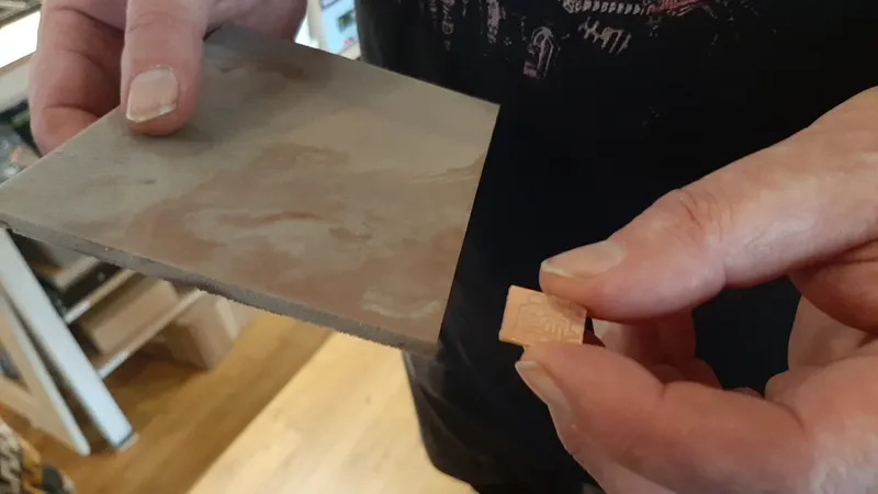
 Milling the outline : I use the same settings as I did for the holes and cut out the board, I use a flat screwdriver to lift the milled board. I clean it with the sticker removal and now I can start the soldering!
Soldering
Before I can solder I need to find the right components. Henk shows me how the wall on component is organized.
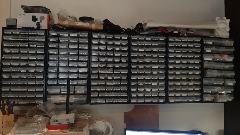 Still look me ages to find everything! here you find al the components, make sure to scroll down a bit. The pictures are very helpful and another thing is look out for is the size of the components. We use the 1206 SMD components you can even go smaller but we can’t solder them by hand anymore.
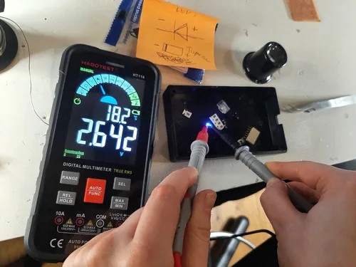
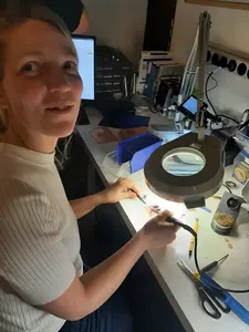
Joe and I than started soldering, starting with the LED’s, Michelle shows us how to measure the plus and minus using the multimeter, my multimeter at home doesn’t have enough power to lighten the LED’s but at Waag it does.
Solder steps
- heat the pads on the board and tin them with a thin layer of tin.
- place the components using tweezers, make use you put them in the right place!
- heat the pad again so the tin of the pad will slightly fasten to the component, do both sides.
- heat the pad once more and put a bit extra thin to fasten the component, you want a volcano shape!
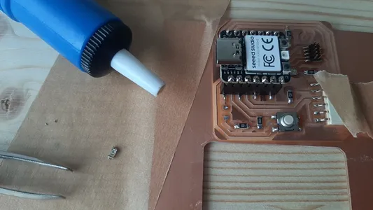
I make a drawing so I wont forget it and continue with the resistors the switch and end with the headers. Here I made a mistake, its better to first put the XIAO RP2040 chip inside the headers and then solder them on your board, this will make sure the chip always first and everything is straight. I didn’t do this and thats why they are a bit crocked but it works. Next time i will definitely use this trick from Henk to solder them properly. It’s already six in the evening so I go home back to Elst and will test the board tomorrow morning.
Testing and debugging
I start testing the board following ardians steps here
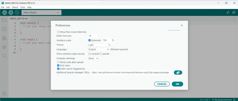
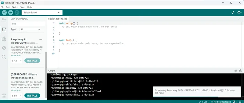
I start with putting the link below in the Arduino IDE -> preferences -> additional boards manager URL’s
https://github.com/earlephilhower/arduino-pico/releases/download/global/package_rp2040_index.json- I download the library Raspberry Pi Pico/RP2040 from earlephilhower
- Open the Blink example. File -> examples -> basics ->blink
- I change LED_BUILTIN for 26 (this is the led pin were the board I made has a blue led)
void setup() {
  // initialize digital pin LED_BUILTIN as an output.
  pinMode(26, OUTPUT);
}

// the loop function runs over and over again forever
void loop() {
  digitalWrite(26, HIGH);  // turn the LED on (HIGH is the voltage level)
  delay(1000);                      // wait for a second
  digitalWrite(26, LOW);   // turn the LED off by making the voltage LOW
  delay(1000);                      // wait for a second
}- Connect the XIAO the board lights up so thats a good sign.
- I verified and pressed upload, the program says it’s uploaded but the LED doesn’t blink..
I use my multimeter to check the connections and it should be right. I’m very confused and want to be sure that the XIAO is actually receiving properly so I program the builtin users LED’s by changing pin 26 into 16 that should be the output pin for the green LED on the board. It’s blinking so the board is receiving properly. I’m now lost. I think maybe I can’t just type 26 as LED pin so I create a const int but of course it’s not helping. I use my multimeter again and check the resistor in Ohm setting. It works fine. I think maybe my LED is broken. I try to light it up just as Michelle showed us at Waag but I can’t because my multimeter does not provide enough Voltages from it self. After 1,5 hour of confusion, I double checked the polarity and see that the LED’s soldered the wrong way around. I was so sure of myself that I did it right. Thats why I didn’t checked it before. Lesson for me: start double checking the obvious things even it you think you did it right. I use my solder iron and solder remover to loosen the LED and solder it in the right position.
It start’s blinking immediately after plugin the board in my laptop. Yay! Learned from this week:
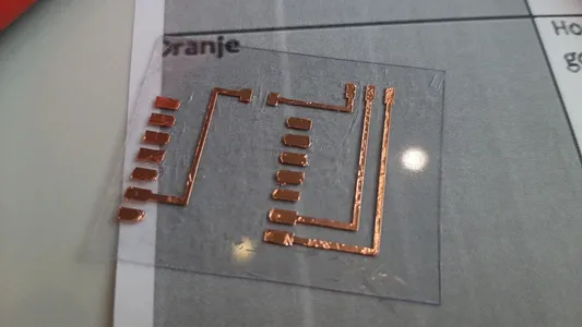
Vinyl cutting tests
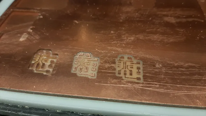
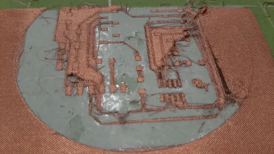
I want to do some test with vinyl cutting coper traces to see how tiny I can make them. I want to cut coper fabric for my final project, see final project page for my coper fabric tests. I test the quentorres design on coper fabric and coper foil. In week 3 I introduce the Summa vinyl cutter I’m using and how to work with it and how I cut coper foil for the febric I used the pressure of 20 gram.
As you can see on the picture, my first try the coper fabric is getting loose. I do a second try and use two sided sticky tape between the coper fabric and the sticky mat.
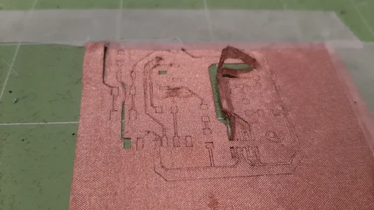
 The traces are to thin and when you weed the material you can see the fabric frays.
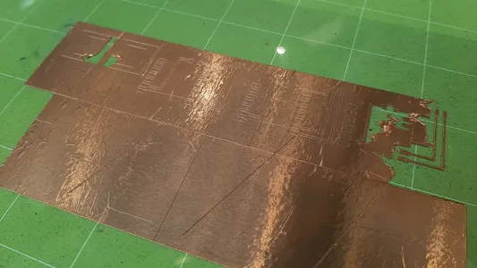
 I decide to try the coper tape. My coper tape isn’t wide enough for the whole design so I redesign the file of Ardian using CorelDraw and make a very easy circuit. For my final project I’m looking in to making a pressure sensor with velostat, for this circuit I need 2 analog pins a ground and the power and it needs one resistor.
 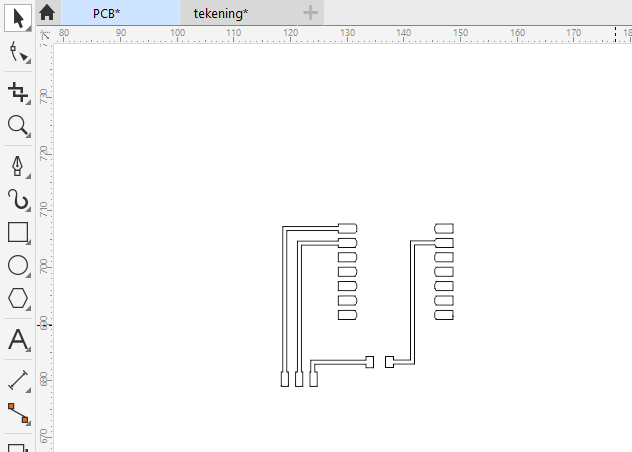 I have made the traces slightly bigger because I experienced so much trouble with the coper fabric and cut the tape. I have some trouble with the knife when it’s traveling (not cutting) that it still cuts because of the stiffness of the cricut sticky mat. I hold down the mat And try again. I put two side sticky pate between it and paste it on a plastic sheet. I weed the design and then test it with my multimeter. Unfortunately one trace is not making proper connection als also I made a mistake with the placement of the resistor. It’s to close to the Xiao board So it won’t fit. I call it a day for now but I learned allot. If I want to use the cutter for my final design I want to design the circuit in KiCad so i don’t make the same mistakes and it’s more properly designed I will also make the traces slightly bigger to prevent mistakes from happening.
Reflection
This week I learned a lot! I had never worked before with a CNC milling machine to make PCB’s. I didn’t know anything about the toolbits, workflow, testings and all that stuff. I made a lot of tests wanting the end result to be perfect but I learned that actually the leveling process has a super big influence of the milled product. And actually a lot of times it’s in the tools not only the settings in MODS. The bit can be broken for example without you noticing it ;)
 Also if it works, it works and using the sponge for deburring works perfectly fine!
I’m very much looking forward in learning how to design my own PCB’s specially now that I have made one from an existing design. I’m not sure what I will do with the XIAO RP2040 but I guess time will tell. An important debugging lesson for me is double check the obvious things even it you think you did it right. I liked working together with Edwin on the group assignment so we could share thought and I also liked that I could work at Waag on friday because of my holiday, soldering al the way to tiny components together with Joe made it a bit more enduring and Michelle and Henk are extremely helpful to ask questions!
I put an effort in my documentation this week, I think it will be very helpful for me to look into it in the future especially if we are going to design PCB’s at the Fablab Arnhem! As a tip I need to try to thing more ahead, especially in stuff I might need in a certain week. I also didn’t try anything with reflow soldering ore making a sheet for it. I want to experiment with this later.
Also if it works, it works and using the sponge for deburring works perfectly fine!
I’m very much looking forward in learning how to design my own PCB’s specially now that I have made one from an existing design. I’m not sure what I will do with the XIAO RP2040 but I guess time will tell. An important debugging lesson for me is double check the obvious things even it you think you did it right. I liked working together with Edwin on the group assignment so we could share thought and I also liked that I could work at Waag on friday because of my holiday, soldering al the way to tiny components together with Joe made it a bit more enduring and Michelle and Henk are extremely helpful to ask questions!
I put an effort in my documentation this week, I think it will be very helpful for me to look into it in the future especially if we are going to design PCB’s at the Fablab Arnhem! As a tip I need to try to thing more ahead, especially in stuff I might need in a certain week. I also didn’t try anything with reflow soldering ore making a sheet for it. I want to experiment with this later.
Feedback: For the vinyl cutter test with curved angles instead of 90 degrees angles to prevent the breakage Try to design a board in KiCad for easier cutting