Week 8
Electronic Design
The group assignment link can be found here
For this week i had to design a cicuit using an EDA tool to design a development board to interact and communicate with an embedded microcontroller, produce it, and test it
I started with choosing an EDA for designing the circuit, KICAD in this case, the reason is KICAD is a beginner-friendly tool, and it also assists beginners with their projects with a much more basic interface, but also the fact that it's an open-source software that permits users as well as developers to improve. I'm using the kicad 8.0.1 that can be dowloaded here
PCB Design
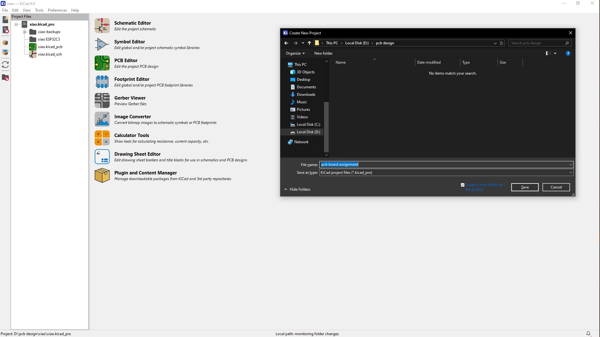
I started designing, first the schematic of the circuit. We start by creating the folder on the desktop where the files will be kept, To create a new project, click on the File menu and select New -> Project Choose where you want to save your project and type in a name for it. Then click on the Save button. The below picture displays creating and saving the new folder and the interface of the KICAD before initiating the design of pcb.
You start off by creating the schematic from the Schematic Layout Editor. Open the editor by double-clicking on the schematic file on the left, or by clicking on the Schematic Layout Editor button

When opening the editor for the first time, you might get asked to Configure the Global Symbol Library Table. Just choose the recommended settings.
Adding components
Your schematic is where you draw your circuit. First, you add the components you want. Then you add wires to show how to connect your components. To add a component, click on the Place Symbol button on the toolbar on the right (or press A on your keyboard), then click anywhere in your work area. This brings up the component chooser.

From the component chooser, you can search for the component you want to add. Just type in what you’re looking for. For example, if you need a resistor, type in “resistor.” Look through the list of results and choose a what you're looking for.
The most important thing is that you choose a symbol that represents the component you want to use in the best way possible.>:
For example, when you search for “resistor,” you’ll get several options like “thermistor,” “trimmable resistor,” and such. But you also get a symbol that is just a resistor, nothing more. So that’s the best representation.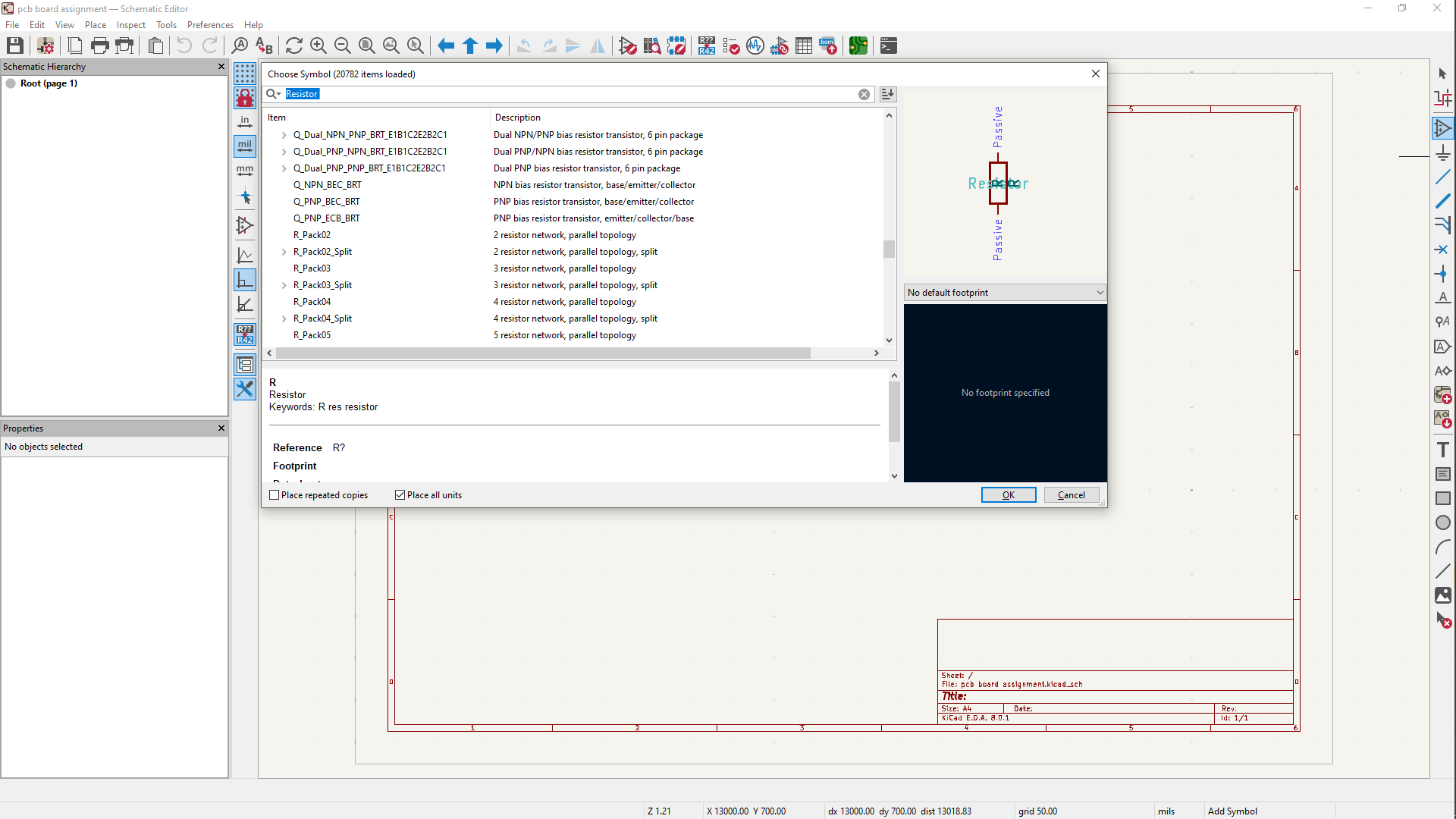
Placing all the symbol
When you’ve chosen a component, place it in your schematic by clicking in your work area with your mouse.
If you later want to move the component, place your mouse pointer over it and press M on your keyboard. To rotate the component, press R. You can zoom in and out by using your mouse wheel or F1 and F2 on your keyboard.
Adding Wires
Now you need to draw wires between the components to connect them. You can do this by clicking on the adding Wires button on the toolbar or by pressing W on your keyboard, so below is the symbol for add wires.
Click on the pin of a component to start drawing a wire. Then click again on the pin where you want the wire to end. If you want to move a component now that they are connected, you have two options: Move and drag.If you place your mouse pointer over a component and press M your keyboard, you Move the component without the wires. But if you press G, you Drag the component with the wires attached. If you start moving or dragging a component but then change your mind, just press the Escape key on your keyboard to release.
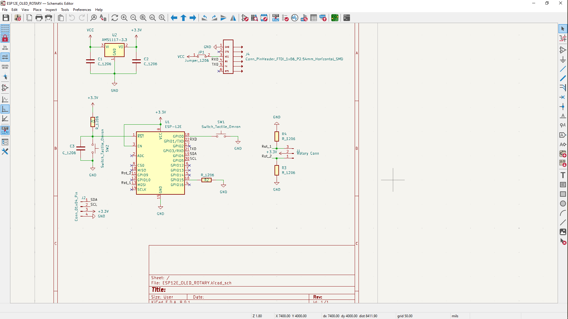
Adding Symbol Values & footprints
In most cases, a component should have a value. For example, a resistor should have a resistance value. A battery should have a voltage value, etc. By pressing V on your keyboard, with your mouse pointer over the component, you can edit its value. You also find this option in the menu when right-clicking on the component.
Note that the value you set for a component does nothing to your circuit. It just serves as a reminder for you, so that you’ll remember what value to use when you build the circuit.
For adding footprints to your components,
The footprint is what will be printed onto the board for each component. For example, for a through-hole resistor,
you’ll choose a footprint with two holes, so that you’ll get two holes for soldering the resistor onto on your board. Click on the
Running the Electrical Rules Check
It’s easy to make errors, like forgetting to connect a component. Especially when you are drawing large circuits. To help you find these errors, use the tool Electrical Rules Check (ERC).
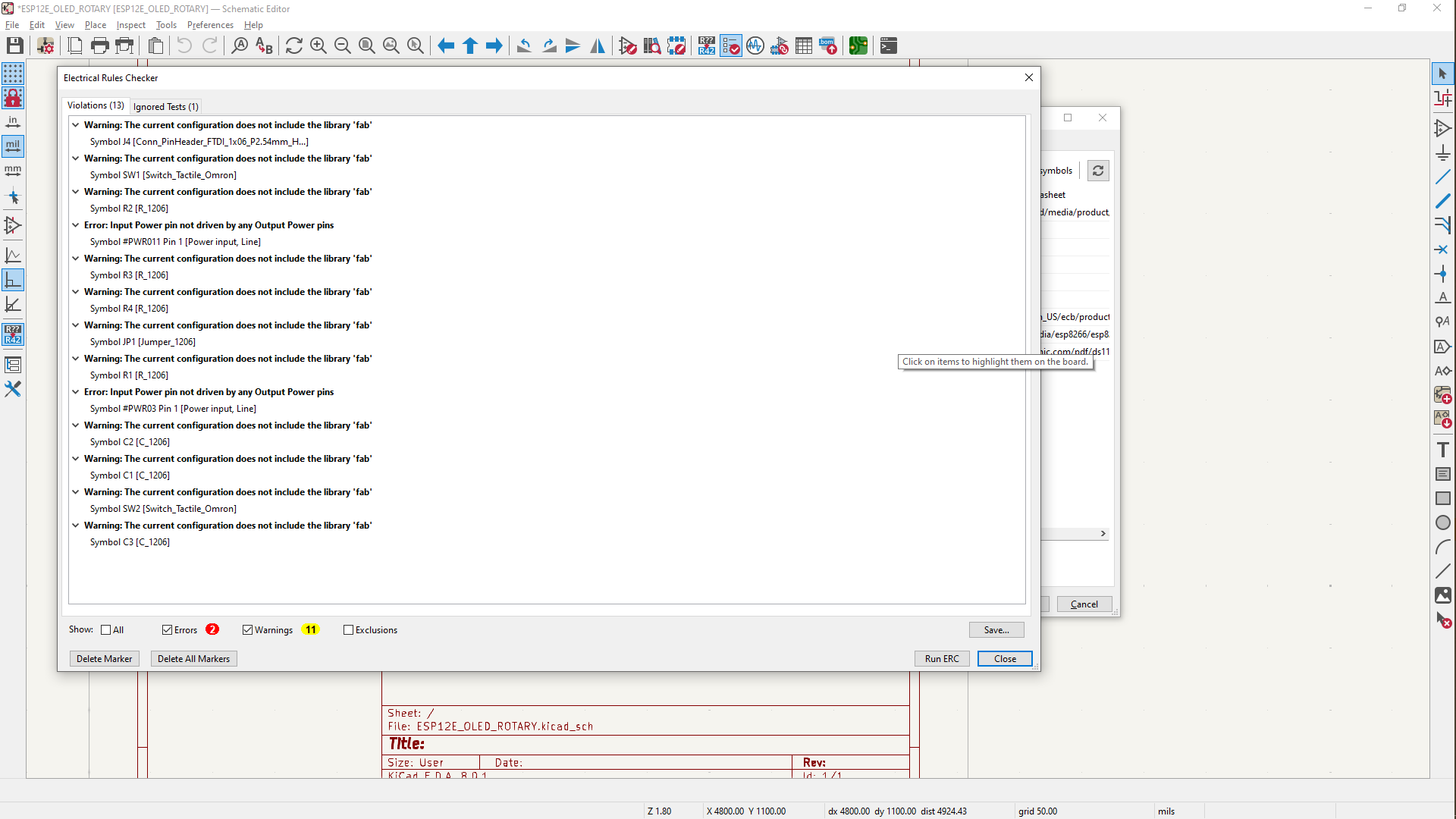
Click on the Inspect menu and choose Electrical Rules Check. Or click on the Perform Electrical Rules Check button, and after running it there were some mistakes i realized, which i then corrected using the symbol Add no connect flags to the pins that were not connected on too.
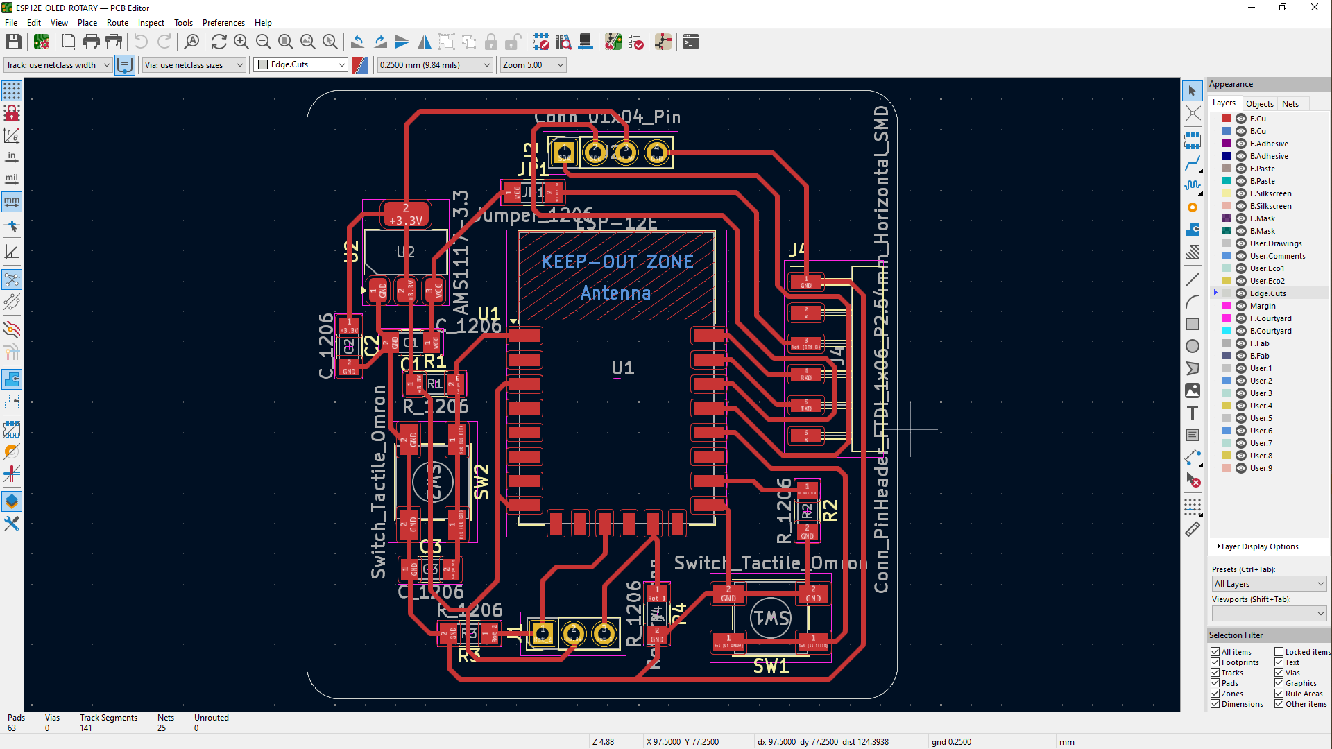
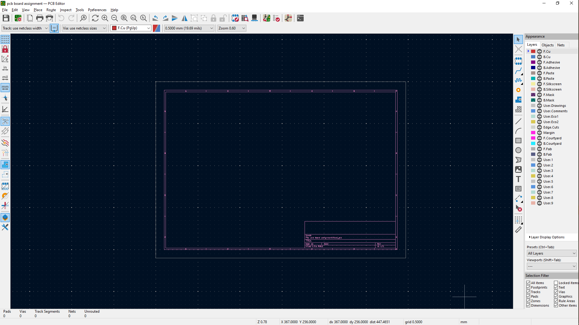
PCB Layout
You have defined how you want to connect the components in the schematic editor, and now it’s time to put that onto your board. You need to decide where to place the components, then draw tracks to create the connections between them. To start drawing your board layout (assuming you’re still in the Schematics Editor), click on the toolbar button that says switch to PCB editor/Open PCB in board editor, as shown below Or go to the Tools menu and select switch to PCB Editor. This opens up the Board Editor window.
The first thing you’ll see is just an empty area. To get started, you need to retrieve information about footprints and connections from your schematic. You can do this by clicking on the toolbar button that says Update PCB from schematic as shown below. You’ll also find this option in the Tools menu.
Keep the default options and click on the Update PCB from schematic button. This will load your footprints. Then click on the Close button.
Click anywhere to place the components.
you zoom in on the components, using either your mouse-wheel, you’ll see white straight lines between the pins. These are called air-wires and tell you which pins to connect according to your schematic but here there are beneath the route track which are the red lines connecting the pins.

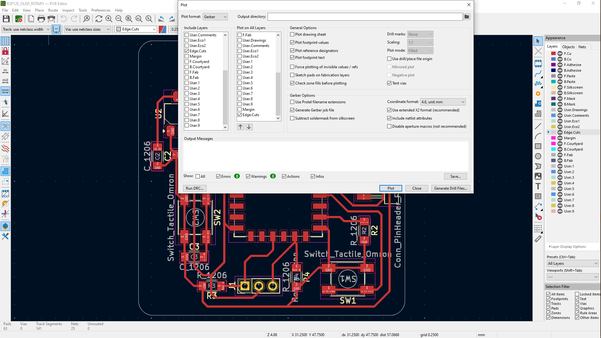
I followed it up with saving the files by going to FILE then plot which opens up a window then first you choose what type of format you would like your work to be saved as by clicking on plot format in the upper left corner, i used svg then next under INCLUDE LAYERS you select F.CU for the top layer to be visible, B.CU for the bottom layer of the PCB this is mostly important when there's a holes to be drilled on the PCB then lastly Edgecuts which for the contour but really then bottom can do both. Right next to it there's another block with the title Plot on all layers under it you'll need to select Edge cuts then click on Plot to save your work, you can also save your work by exporting your work through export by going to files ,export then export files as SVG this will open up a window then you'll click on export below in the output message box you' ll see notification showing you where the files are saved.
Generating Files for machining
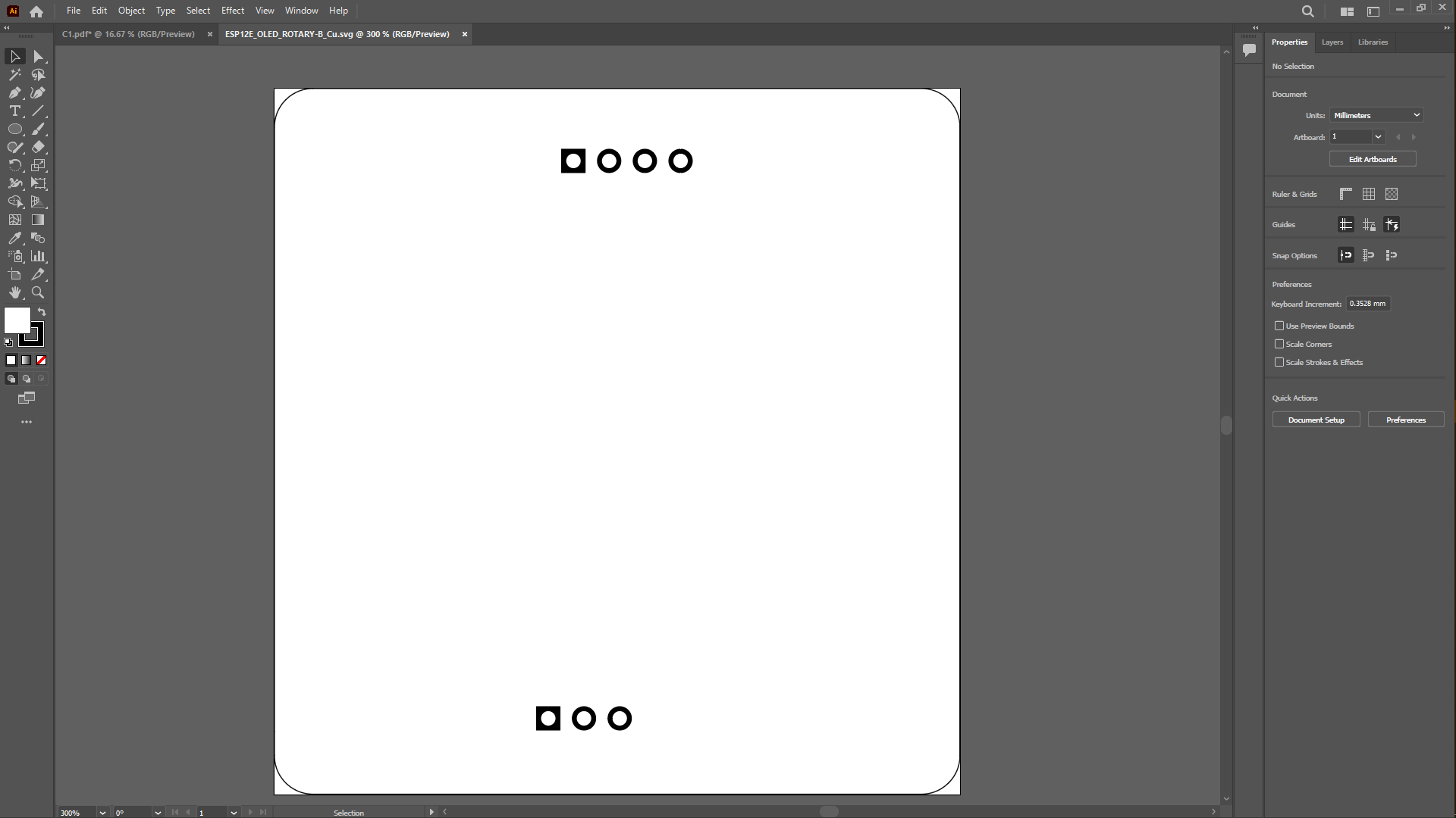
after saving files i had the option of directly generating files for the milling machines but it easy for me to use the png files so i went to use the illustrator software to change the SVG files into PNG files. First you open illustrator then you drag and drop the svg files or you go to files and open then search where you saved the svg files then after its opened in illustrator, you should first know that the file F.CU is for front of the pcb as explained above so it should be looking like the picture below.
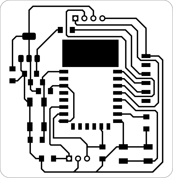
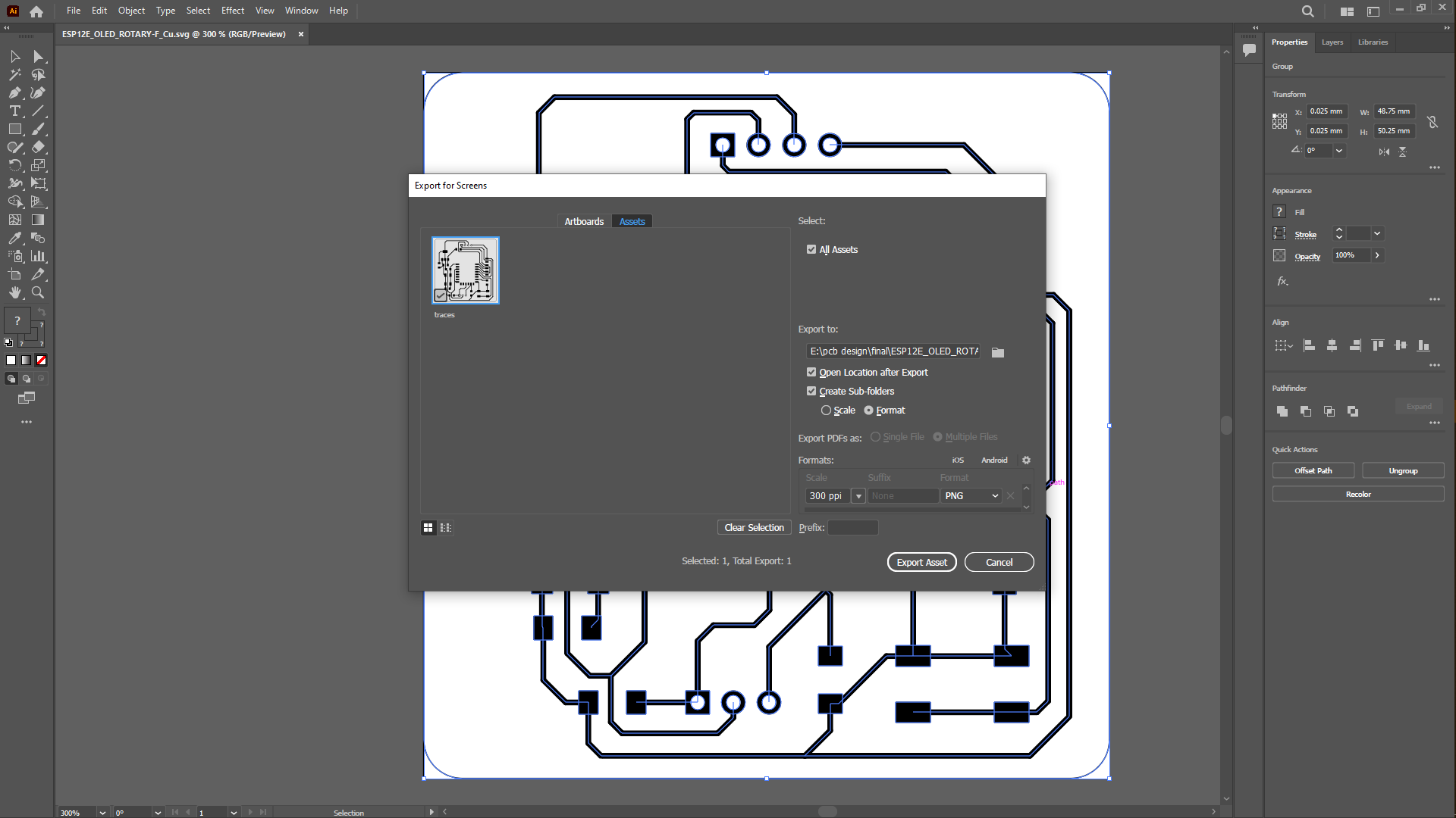
So after it's opened you select everything, right click on the selection, scroll down to Export selection which opens ups a window for export for screens, now you have the file you selected under the name asset 1 which you'll rename the name you want, i named it FRONT@300x, on the right side i choose where to save it under export to, andthen under formats set the resolution300PPI and choose the file type to be PNG then i clicked on export asset to save it. Now you can do the same procedure for each file.
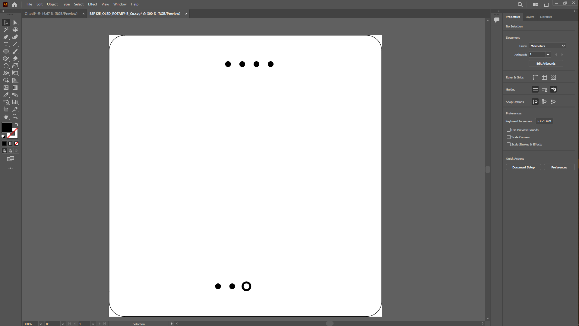
For drills or holes to be drilled on the pcb, there's a little edit to be made, so you open the svg files in illustator then you ungroup everything then we have two shapes the bigger circle with the black fill color and the small one with no fill color, now on my end i firstly deleted the bigger circle/square or the outer shape with the black fill then i changed the circle with no fill color to black fill color i did this so that when i use the MODS to generate files for the milling machine holes to be drilled are small rather than big which can be an issue while milling or can leave the final pcb damaged so below i"ll add the png files generated
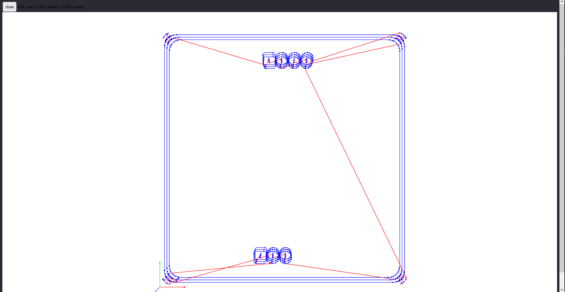
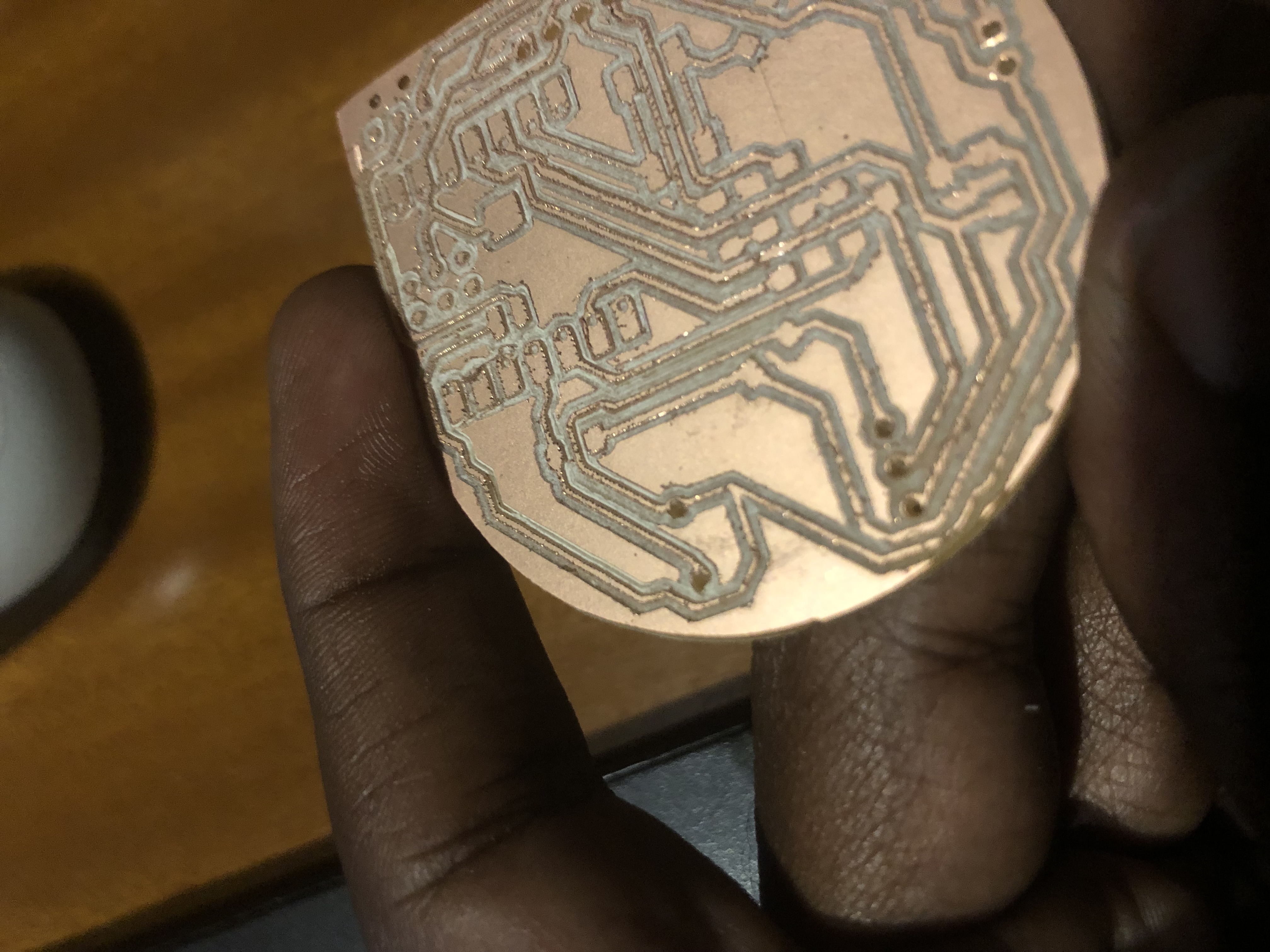
Below i will be sharing different outcomes depending on two options i used to come to a conclusion of always using the method i use of producing a small holes on the output of the PCB so if i load svg files directly into mods, this what i will get as a result: let's take it from this ciruit board
So if use svg files shown in a picture above to create toolpaths for drill directly in mods, this is the later result i get which end up making bigger holes on the pcb
Whereas when i use illustrator and remove the the black outside hole and change the inner white hole to black then use it in mods as, it gives me perfect drills shown below

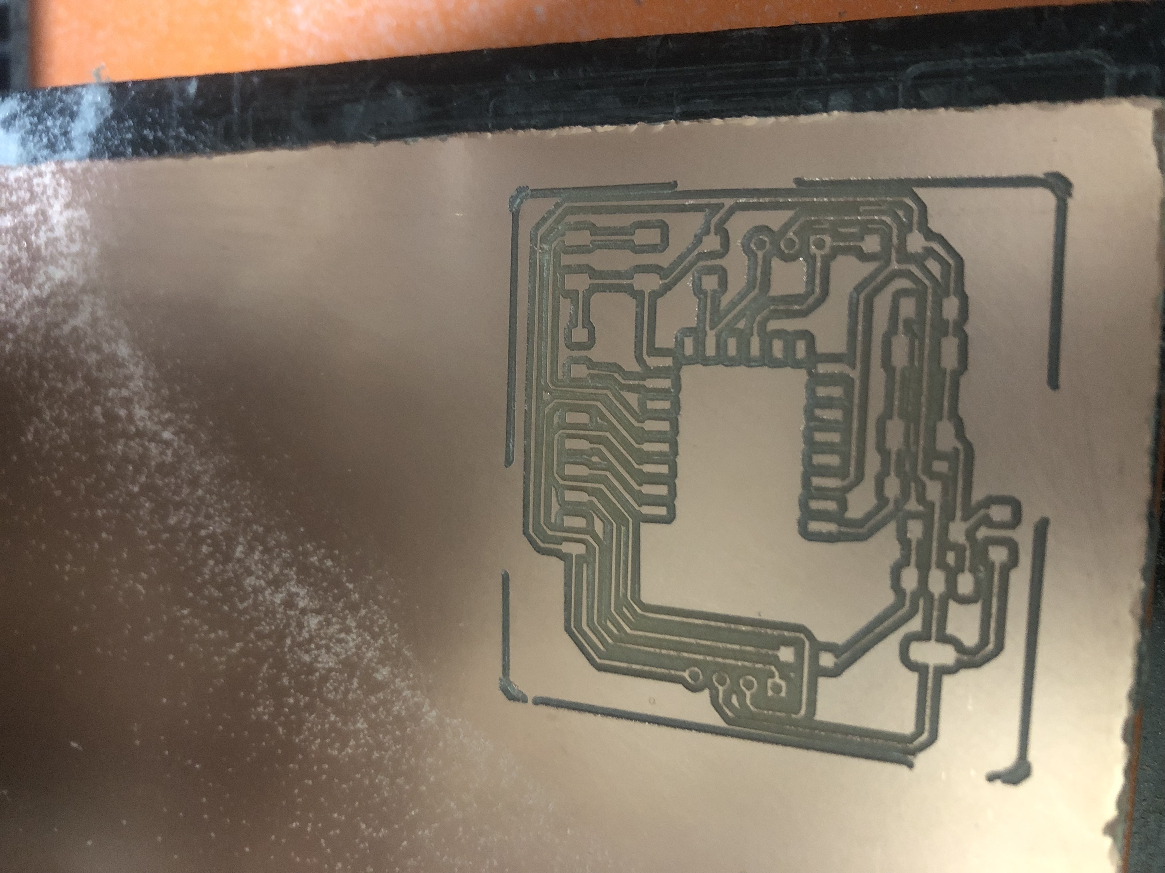
Next, i added the png files to the mods website to generate milling machine files, and our lab is equipped with the roland srm 20, so when you open the MODS then right click on the blue-red icons in the top left upper corner, you then scroll down to click on programs which opens up another list of menu then you scrool down to open program, this brings multiple options or machines you scroll down to find the machines your lab uses in my case i scrolled down to select under ROLAND, SRM-20 MILL then under it select MILL2D PCB then with the system open i go under read png, i clicked on select png file, after it has been loaded you click first on Invert then click on mill traces 1/64 under set pcb defaults, next then click on calculate, the process is the same for edge cut and drills expect that these type of files we use mill outline instead of mill traces, so after clicking on calculate its gonna automatically save the file, an rml type file for the milling machine.
i saved the file then put it on flash drive, connected it to the machine that has the roland srm-20 software for milling then loaded the files to be milled so first the traces the drills (for drilling hokes) then edge cuts for removing the pcb
below there's a picture of traces, after this i moved to adding components and soldering next was to start uploading codes to the microcontroller.
ADDING CODES TO THE MICRO CONTROLLER
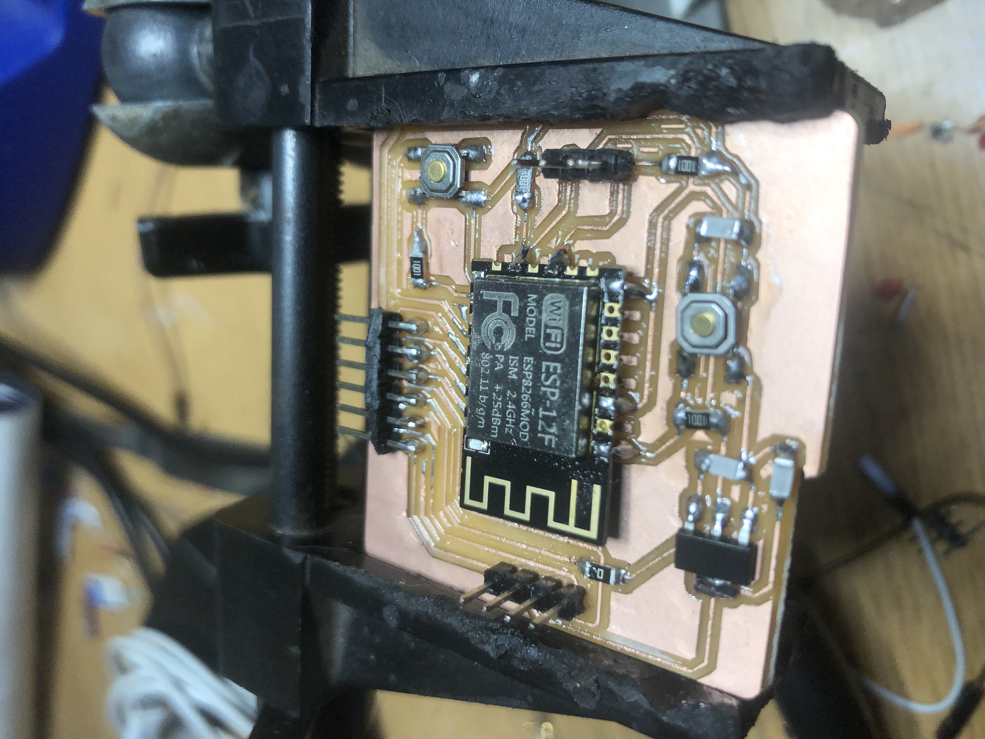
For the microcontroller i used the ESP8266MOD and as you can see in this circuit i also have two switches one for resetting the micro controller and the other for booting i also have pin headers for rotary encoder on one sisde and the oled on the other side because i intended to use this for both output devices but also input devices but also intended that i will be using this circuit for interacting the two devices through the micro controller.
so after soldering, with the help of a ftdi cable, TTL-232R-5V i managed to connect it to the computer to upload codes i used the arduino ide due the facts that it was beginner friendly and also easy to use
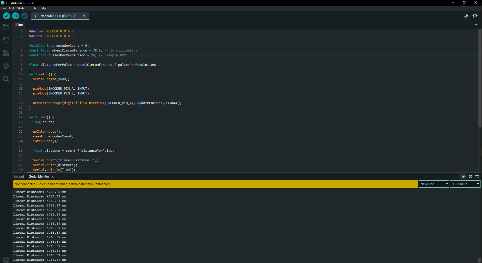
ARDUINO CODES FOR ROTARY ENCODER
        #define ENCODER_PIN_A 8
        #define ENCODER_PIN_B 7

        volatile long encoderCount = 0;
        const float wheelCircumference = 78.5; // in millimeters
        const int pulsesPerRevolution = 24; // Example PPR

        float distancePerPulse = wheelCircumference / pulsesPerRevolution;

        void setup() {
          Serial.begin(9600);

          pinMode(ENCODER_PIN_A, INPUT);
          pinMode(ENCODER_PIN_B, INPUT);

          attachInterrupt(digitalPinToInterrupt(ENCODER_PIN_A), updateEncoder, CHANGE);
        }

        void loop() {
          long count;

          noInterrupts();
          count = encoderCount;
          interrupts();

          float distance = count * distancePerPulse;

          Serial.print("Linear Distance: ");
          Serial.print(distance);
          Serial.println(" mm");
          delay(1000);
        }

        void updateEncoder() {
          int stateA = digitalRead(ENCODER_PIN_A);
          int stateB = digitalRead(ENCODER_PIN_B);

          if (stateA == stateB) {
            encoderCount++;
          } else {
            encoderCount--;
          }
        }
so due to my board that i had used being completely unusable i decided to re use the xiao ESP32-C3 since i had used it before so i connected the encoder pins to the XIAO_ESP32C3 and it wasn't the first time using it so the board was already installed in the arduuino IDE all i had to do is configure my rotary pins and load the current codes in the microcontroller
Short Hero video
Assignment Files