Use the test equipment in your lab to observe the operation of a microcontroller circuit board Send a PCB out to a board house
Use an EDA tool to design a development board to interact and communicate with an embedded microcontroller, produce it, and test it. Extra credit: try another design workflow Extra credit: design a case for it Extra credit: simulate its operation
Preparatory activities for the group assignment were meticulously carried out, ensuring thorough preparation for collaborative work. The specific activities conducted on particular dates are outlined below:
13/03/2024: Fab Academy classes were conducted, during which the week was organized, and materials and tools necessary for the group project were prepared.
15/03/2024: A variety of tools were utilized to perform group tasks, accompanied by comprehensive research on their usage and applicable measurements.
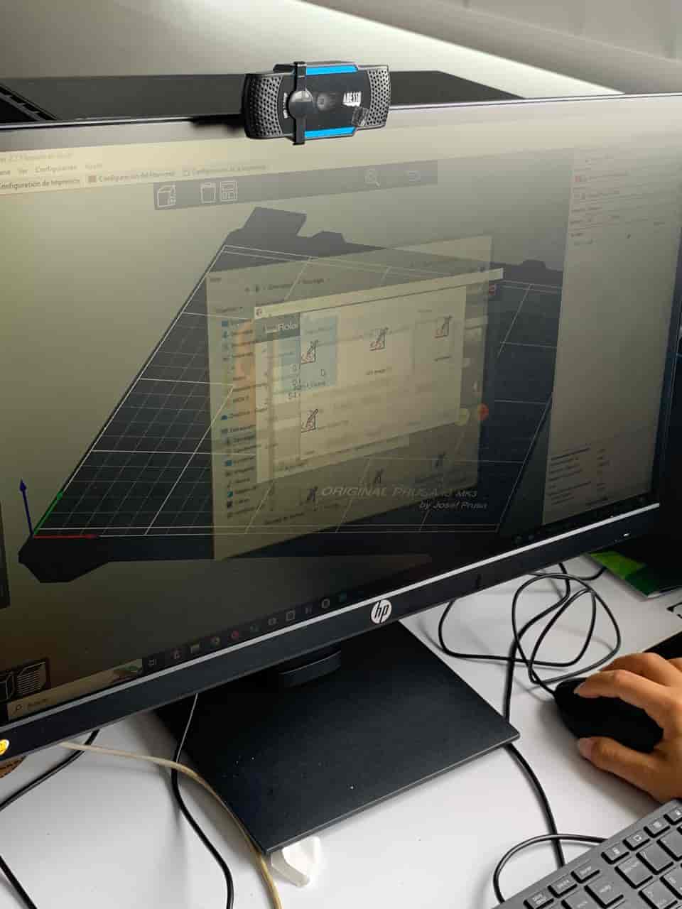
16/03/2024: Training on KICAD was received through the OPEN GLOBAL TIME platform, providing a solid theoretical framework for PCB design.
17/03/2024: Detailed documentation of all progress and advancements made to date was carried out, ensuring a comprehensive record of the activities undertaken.
18/03/2024: Meticulous design of the printed circuit board (PCB) was undertaken, incorporating the knowledge acquired during previous training sessions.
19/03/2024: The fabrication of the printed circuit board was completed according to the specified design requirements, thus concluding the preparatory activities and paving the way for the development of the group assignment.
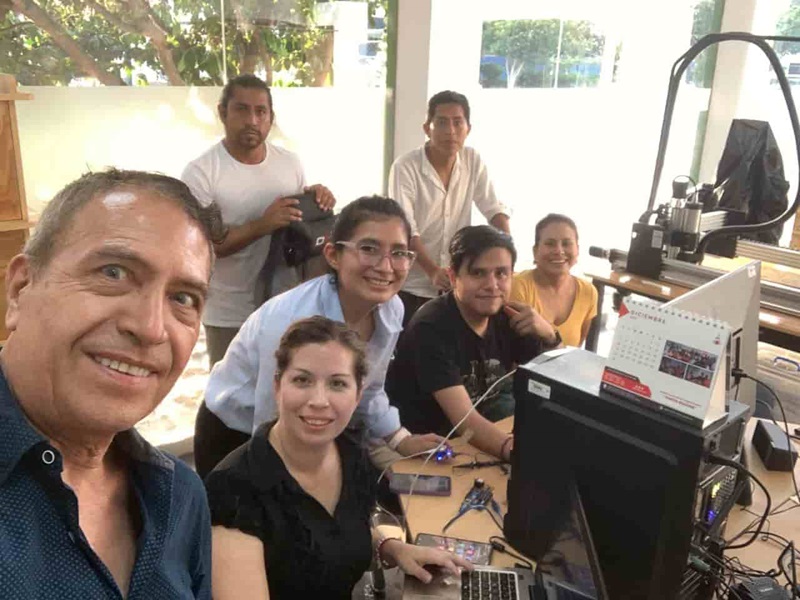
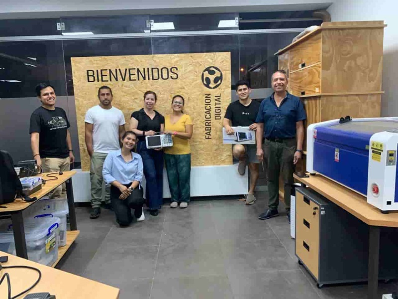
During the development of the group assignment, the resources available at the Simon Bolivar Institute were leveraged, thanks to the efforts made by Grace before the relevant authorities.
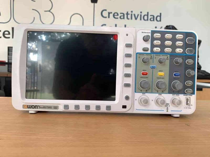
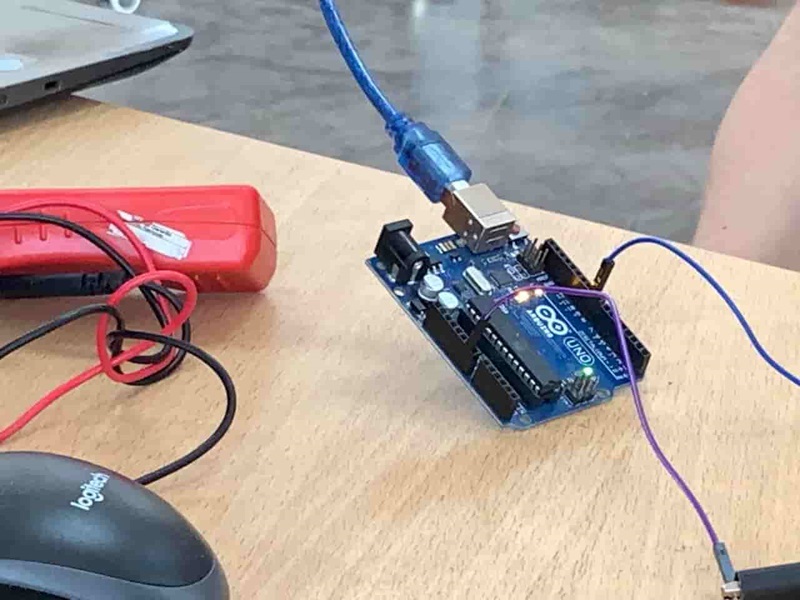
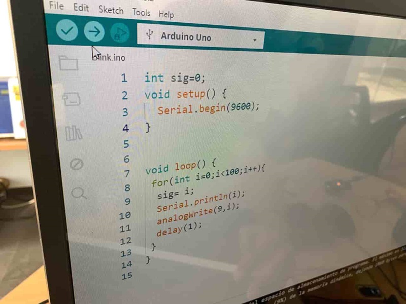
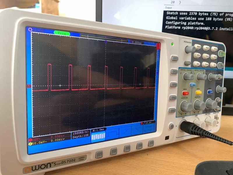
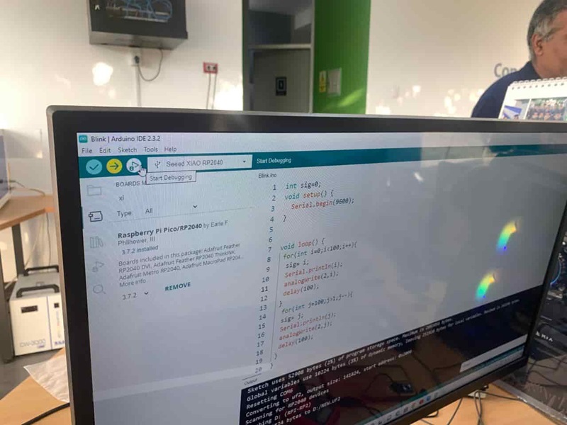
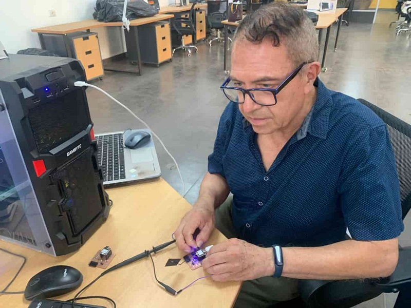
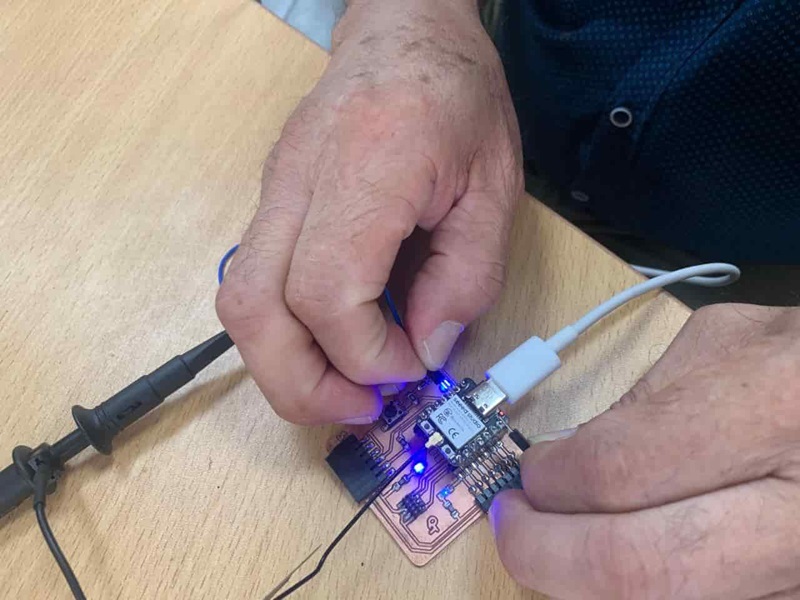
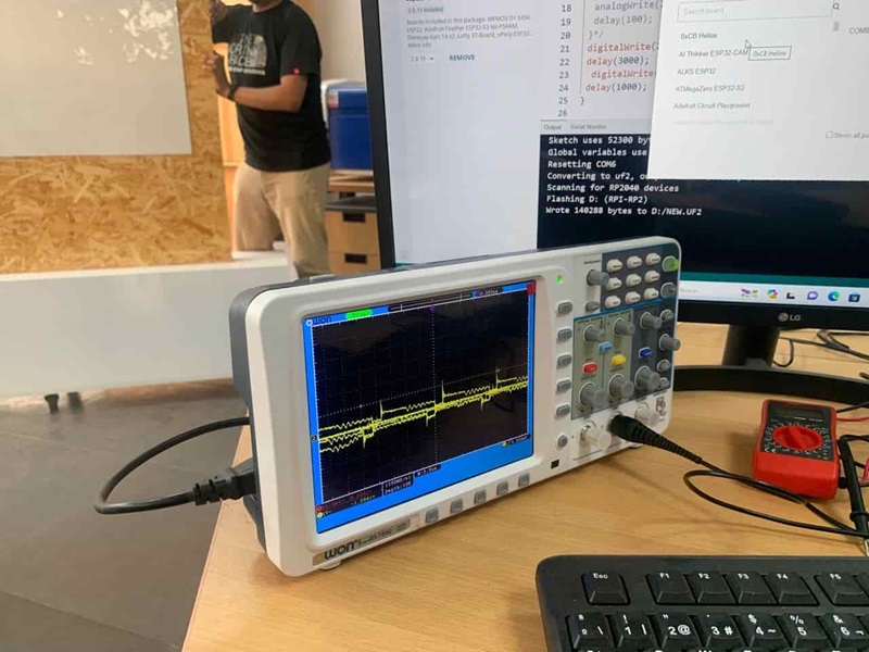
Measurements of signals generated by the XIAO microcontroller were conducted using the OWON Smart oscilloscope, with the aim of obtaining precise data on its functioning.
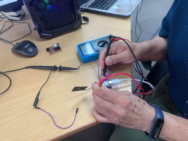
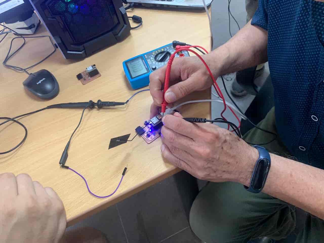
Measurements of voltage drop across LEDs and resistors were performed, verifying Kirchhoff's second law using a Fluke voltmeter, thus ensuring the integrity and accuracy of the results obtained.

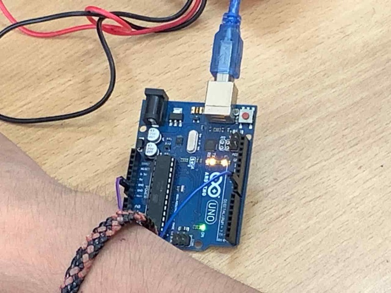
A series of tests were conducted using the multimeter, starting with the verification of the polarity of DIP and SMD LEDs, followed by resistance measurements to determine their nominal value and suitability for the proposed design.
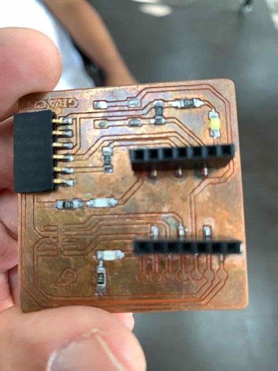
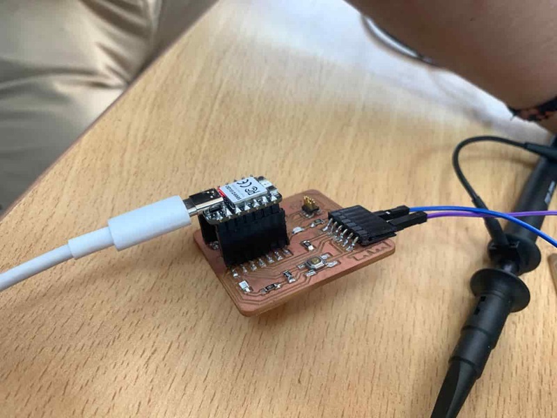
A continuity test was performed on the QUENTORRES developed in previous weeks, using the multimeter to confirm the connectivity of the components and ensure their proper functioning.

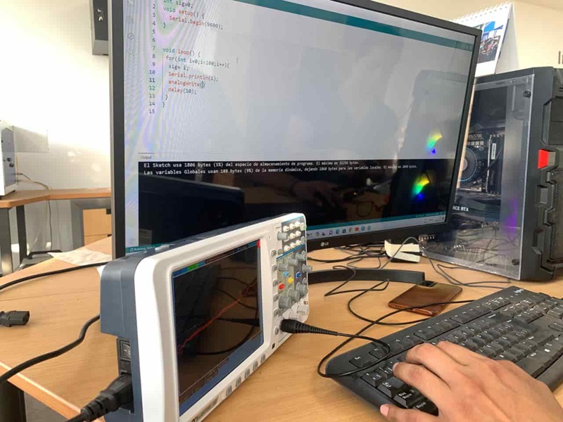
Subsequently, the oscilloscope was applied to analyze the electrical signals of the QUENTORRES board, allowing for a deeper understanding of its behavior and performance.
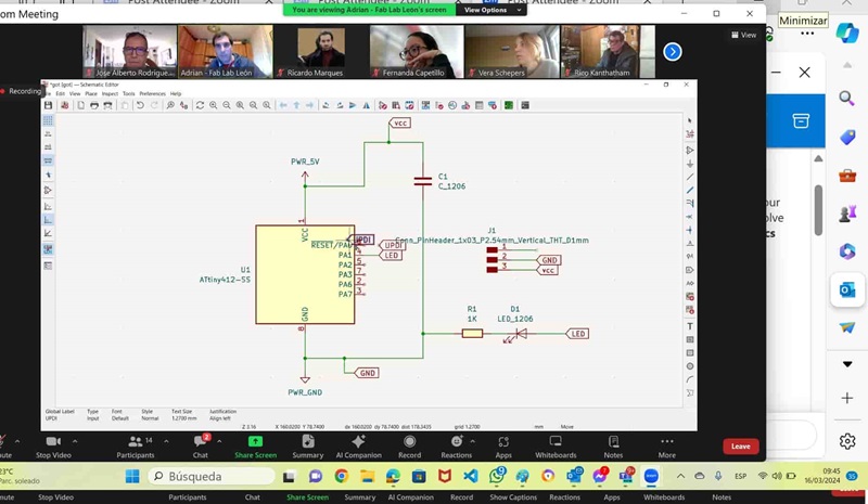
For the development of the electronic design, the KICAD platform was employed, known for its robustness and versatility in creating printed circuits. Below are the detailed steps followed during the design process:
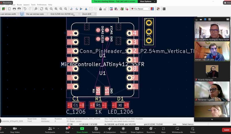
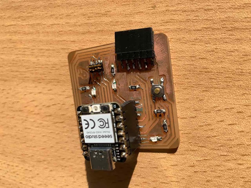
The design commenced by locating the XIAO RP2040 microcontroller in the KICAD component library. I opted for version 2 of the QUENTORRES, featuring vertical connectors for flexibility in its arrangement.
Next, the required voltages for the XIAO RP2040 (3.3V, 5V, and GND) were integrated into the electrical schematic, establishing clear and precise connections between the microcontroller and associated elements.
Labels were assigned to the pins of the XIAO RP2040 for identification, ensuring a clear visual reference throughout the process. Each connection was meticulously verified for correctness to avoid potential errors that may compromise the final design.
Additional complementary components were added to the design, such as a tactile switch for HAPPLE, as well as standard 1206 resistors and LEDs, selected from the FAB ACADEMY library to ensure compatibility with the corresponding footprints.

Connections between components were routed, paying special attention to power points (5V, 3.3V, and GND) to ensure optimal circuit operation. Proper network formation was verified to ensure design integrity.
Upon completion of the electrical schematic, PCB design commenced. The PCB editor in KICAD was opened, and the design was updated with changes made in the schematic. Components were efficiently arranged, and connection traces were laid out.
Trace widths were configured based on the requirements of each connection. Widths of 0.8 mm were used for power points, and 0.4 mm for other pins, ensuring adequate conduction capacity and minimizing interference between traces.
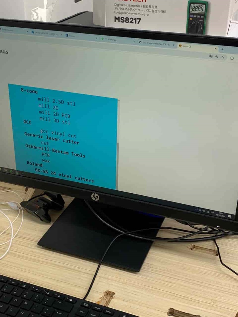
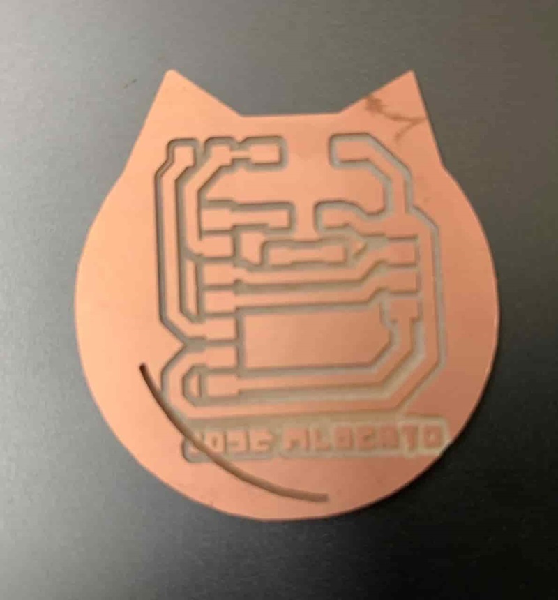
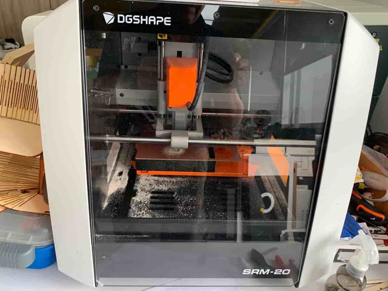
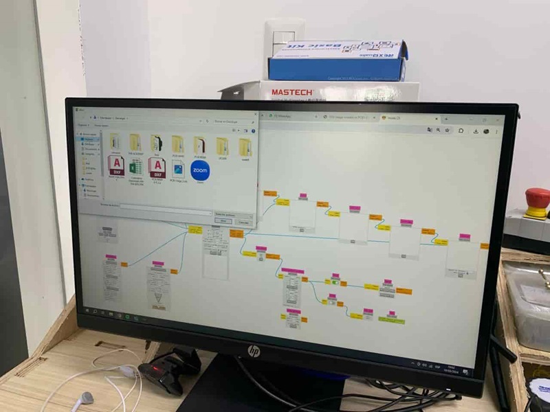
After component arrangement and trace creation, the design was exported to MODS.CE for subsequent milling. The design was converted to SVG format and imported into the MODS.CE platform, where milling parameters were configured, and the accuracy of the work to be performed was verified.
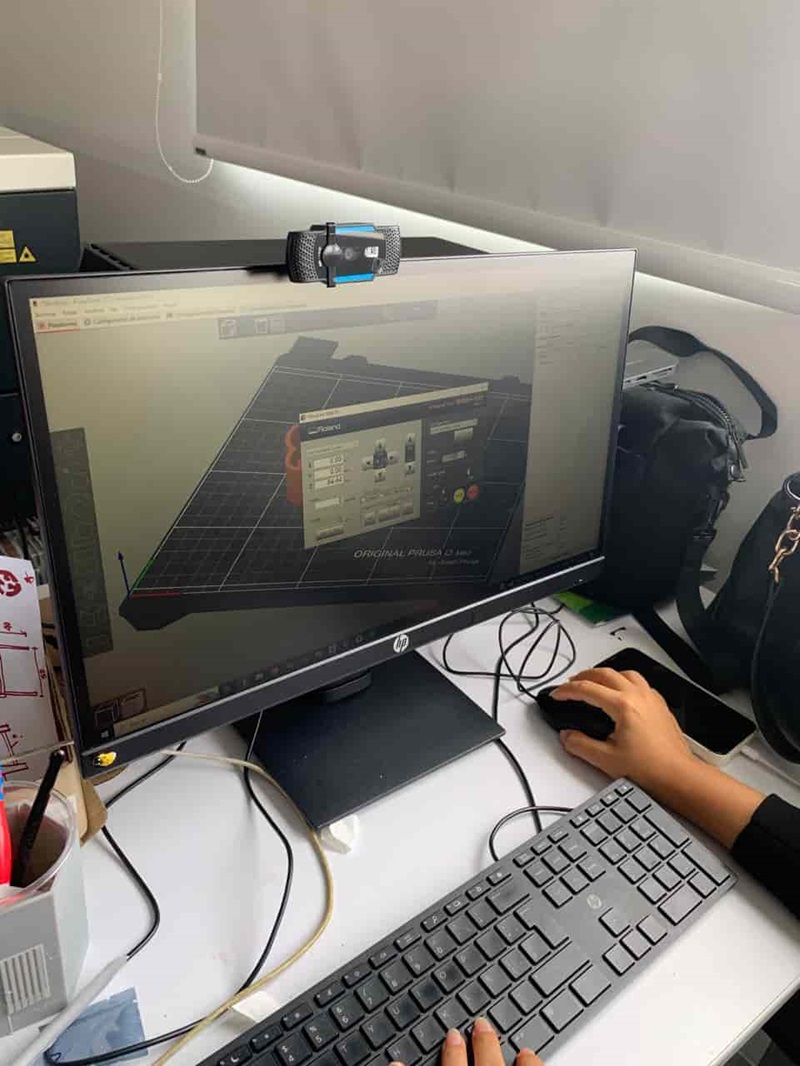
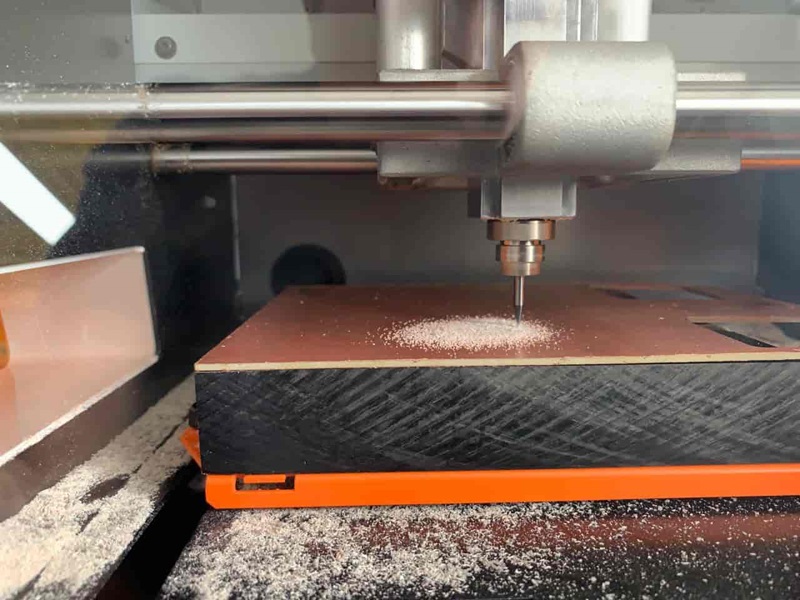
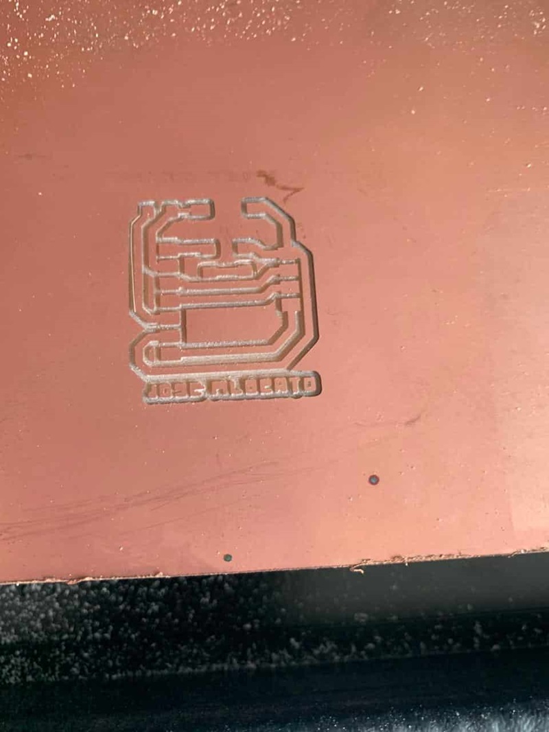
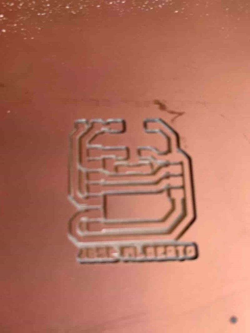
Finally, PCB milling was carried out following instructions provided by MODS.CE. A preview of the milling path was generated for validation, and the final file was downloaded for import into the milling software used.
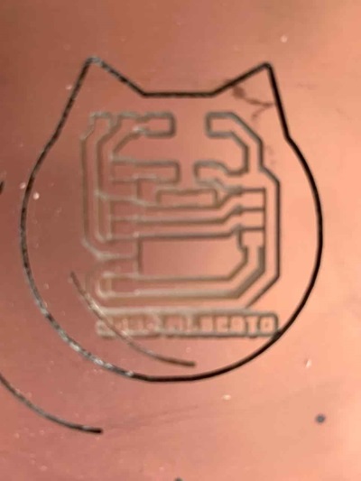

The milling process was completed for both the traces and the board edge. The integrity of the milled PCB was verified, and a visual inspection was conducted to ensure the quality of the final result.