
These design rules will provide a solid foundation for in-house PCB (Printed Circuit Board) production, ensuring consistency, efficiency and quality throughout the development and manufacturing process.
In-house PCB production requires careful planning and establishment of design rules to ensure process efficiency, quality, and feasibility. Below are the fundamental rules that will guide the internal PCB design:
Establish adequate spacing between tracks to prevent short circuits and ensure signal integrity.
Ensure an efficient and orderly layout to optimize space on the plate and facilitate manufacturing.
Define standard plate dimensions to maximize efficiency in production and material use.
Avoid complicated shapes that may increase costs and complexity of the manufacturing process.
Establish clear tolerances to ensure accuracy in component positioning and track connection. Define manufacturing tolerances for plate drilling and routing.
Specify board materials according to circuit requirements and environmental conditions. Consider the availability and ease of acquisition of materials to ensure consistent production.
Limit the number of layers based on the complexity of the design to maintain economic viability and simplify manufacturing.
Clearly define the function of each layer and establish rules for the connection between them.

Include markers and labels to clearly identify components, connections and references.
Establish a standard for marking component polarities and values.
Maintain safety distances between components to prevent electromagnetic interference and ensure circuit reliability. Comply with applicable electrical safety regulations and regulations.
Define standard sizes and locations for mounting holes and holes. Ensure mounting holes are robust enough to withstand assembly and end use.
Establish rules for the width of pathways and connections to accommodate the current and minimize resistance. Avoid unnecessarily long trace paths to reduce inductance and improve performance.
Comply with internal and external production regulations and standards. Document and periodically review design rules to ensure continuous adaptation to emerging technologies and industry best practices.
This process ensures that the microcontroller development board meets project requirements and operates reliably, providing a solid platform for the development and testing of additional microcontroller-based projects.
Identify the project requirements, such as the choice of microcontroller, the necessary interfaces (USB, UART, etc.), and the peripheral components (LEDs, buttons, sensors) that will be included on the board.
Create the development board schematic using circuit design software. Include the microcontroller, power connections, communication interfaces and necessary peripheral components.
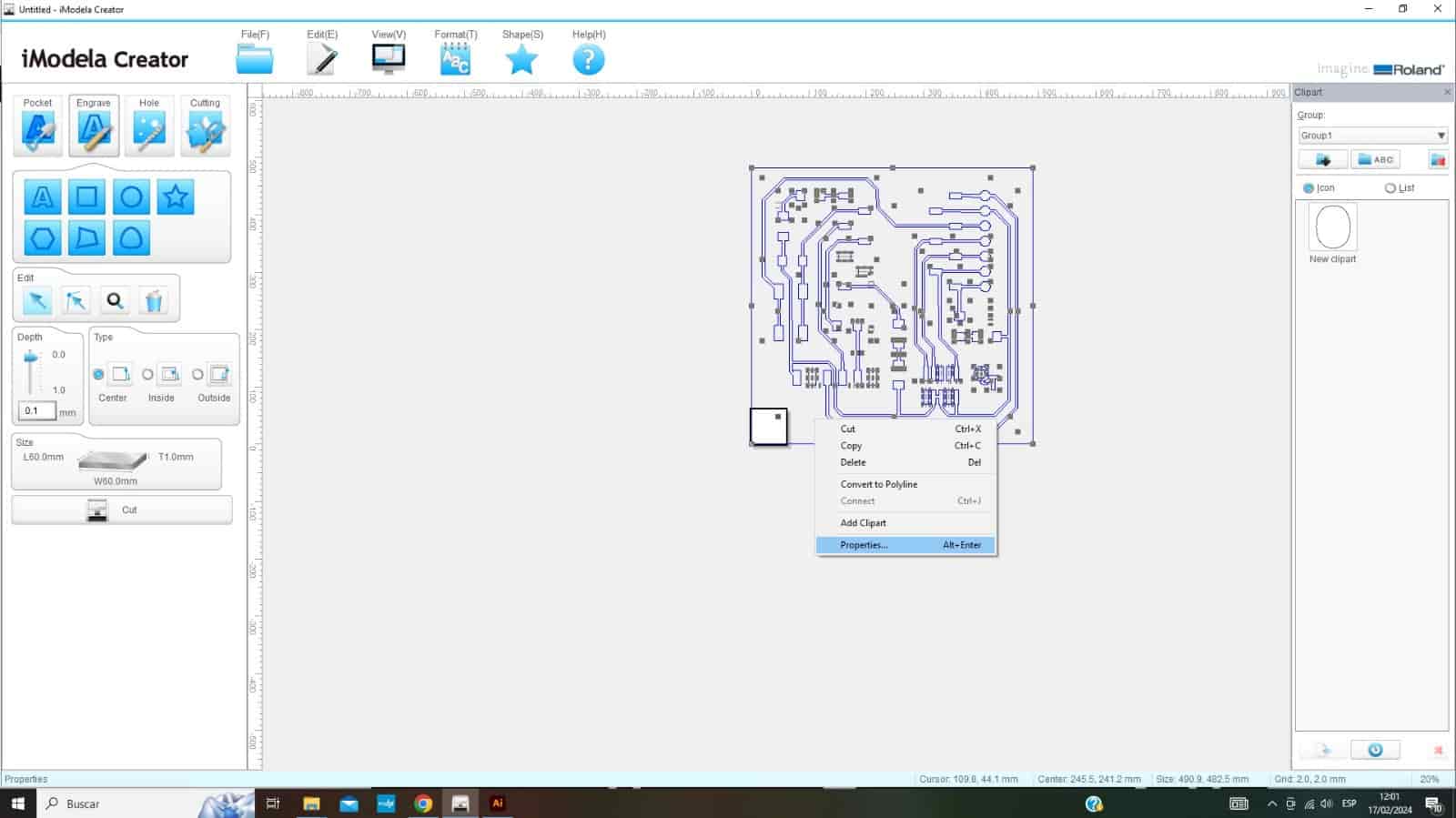
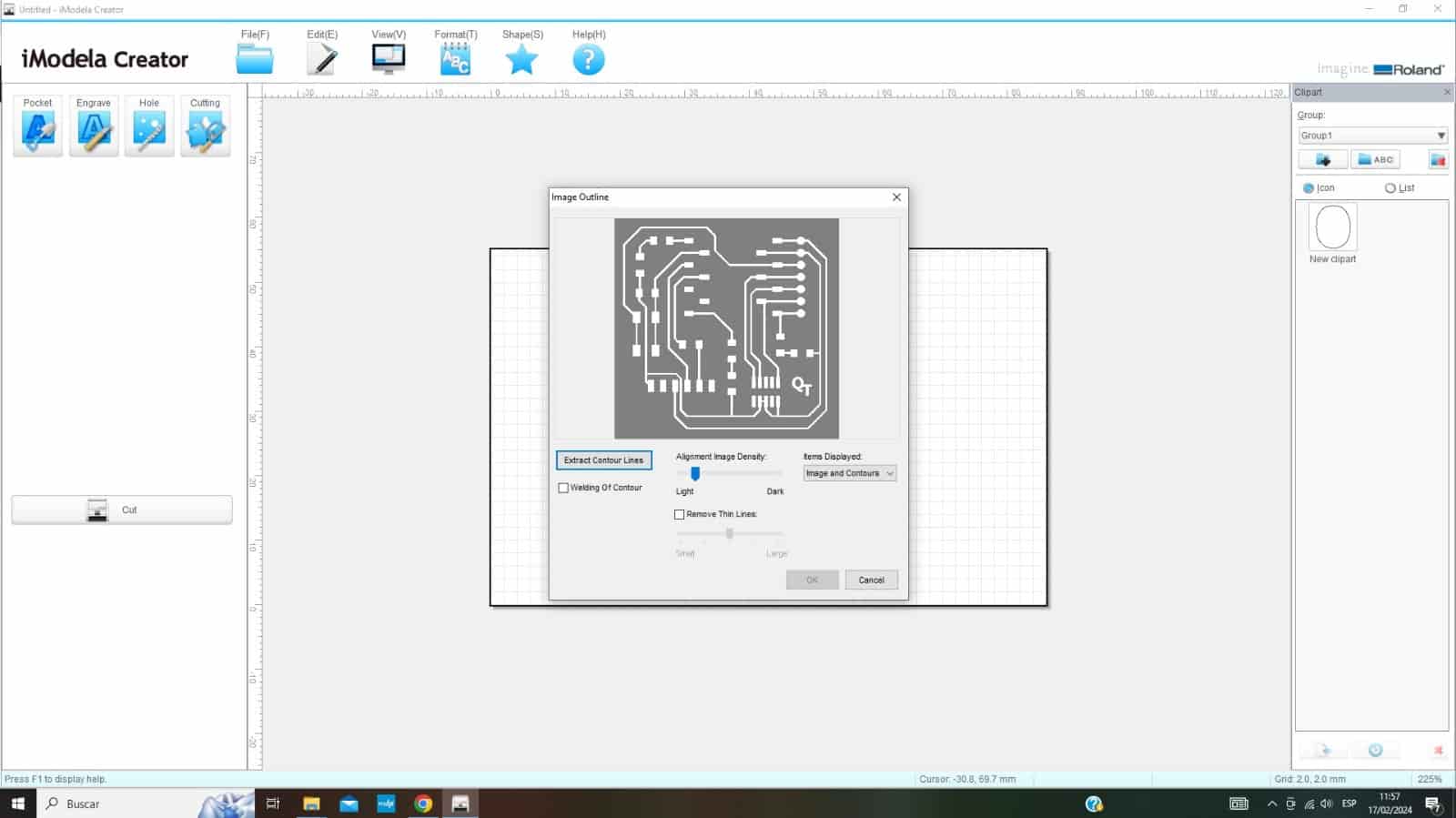
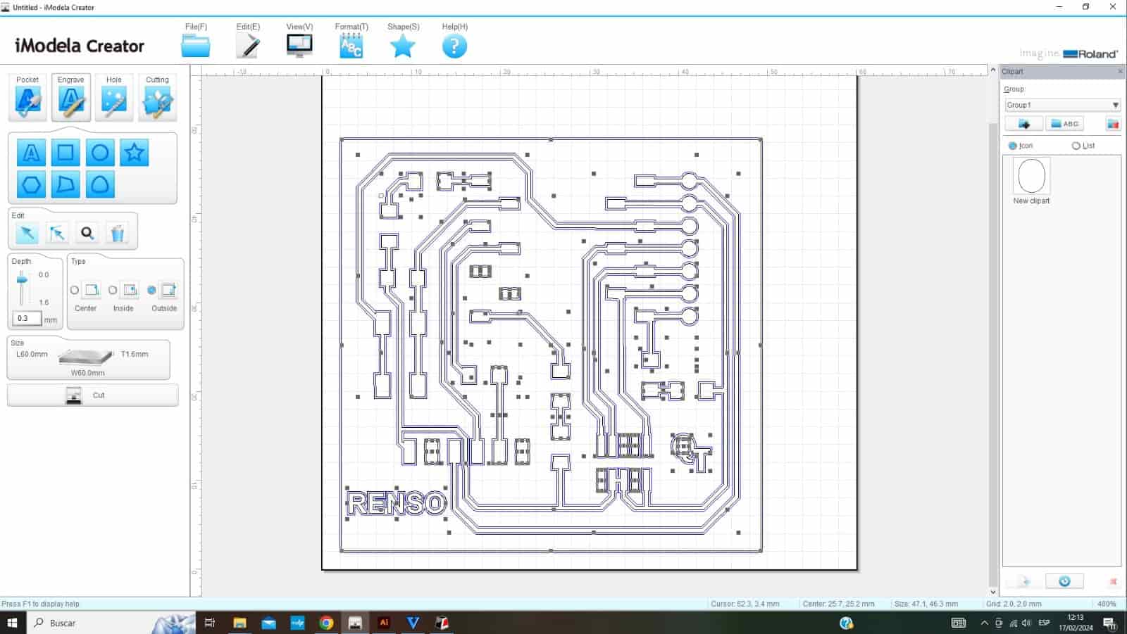
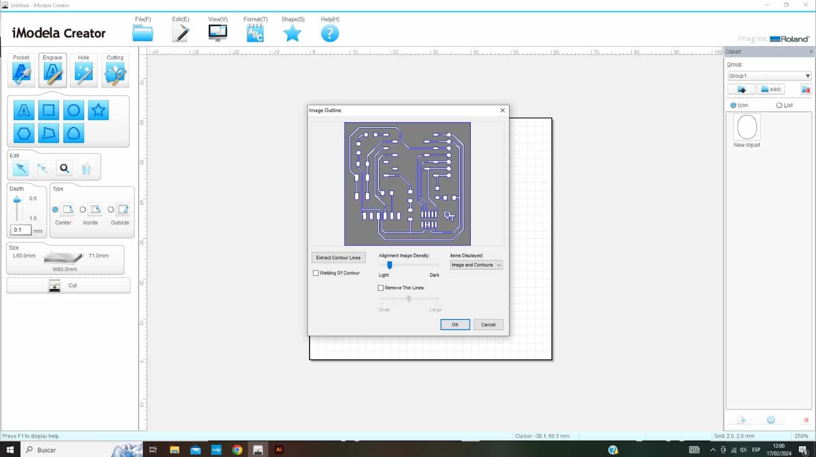
Use the schematic as a basis to design the PCB (Printed Circuit Board) layout, placing and routing the tracks efficiently. Consider the location of components to facilitate assembly and connection.
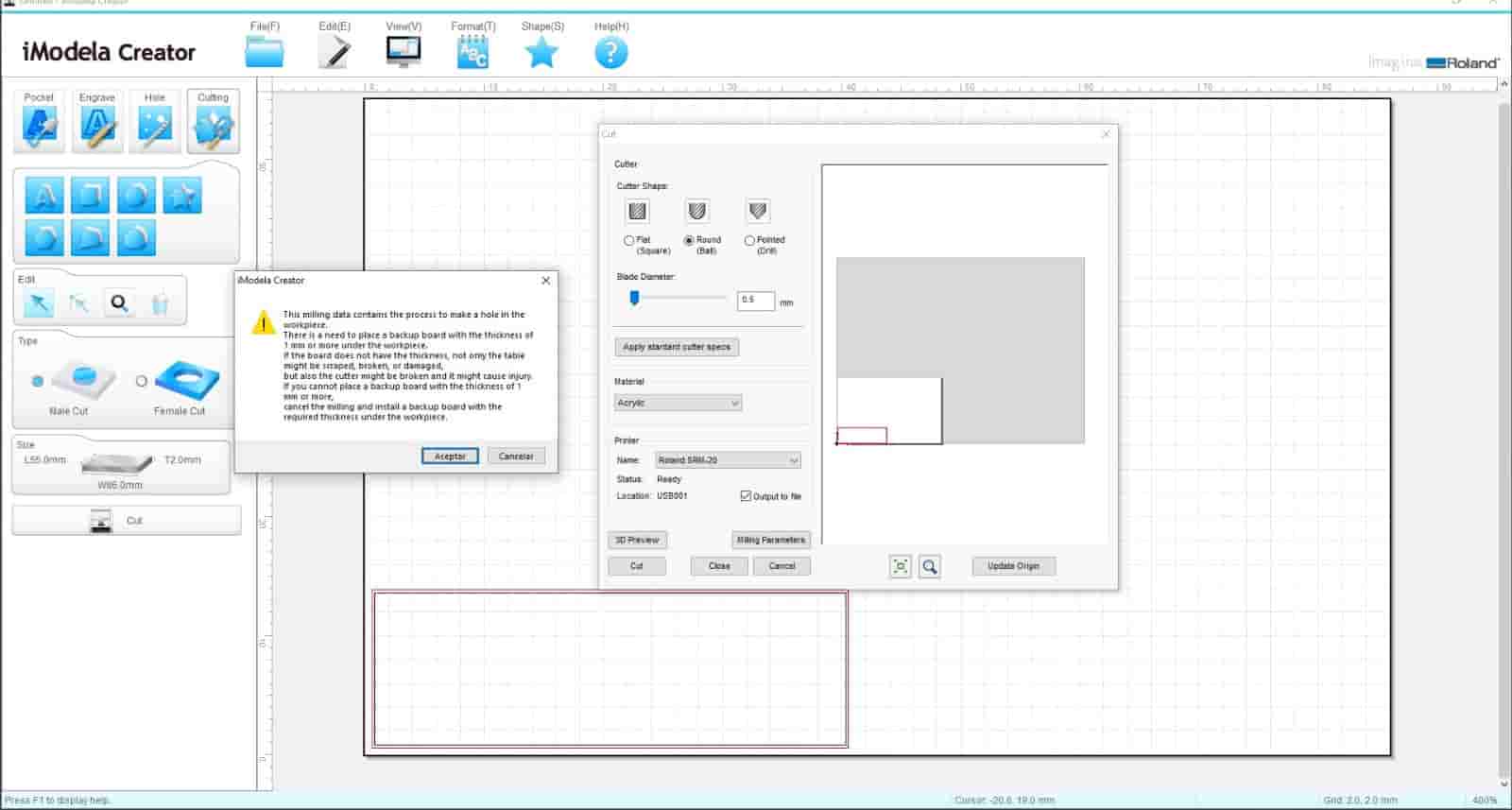
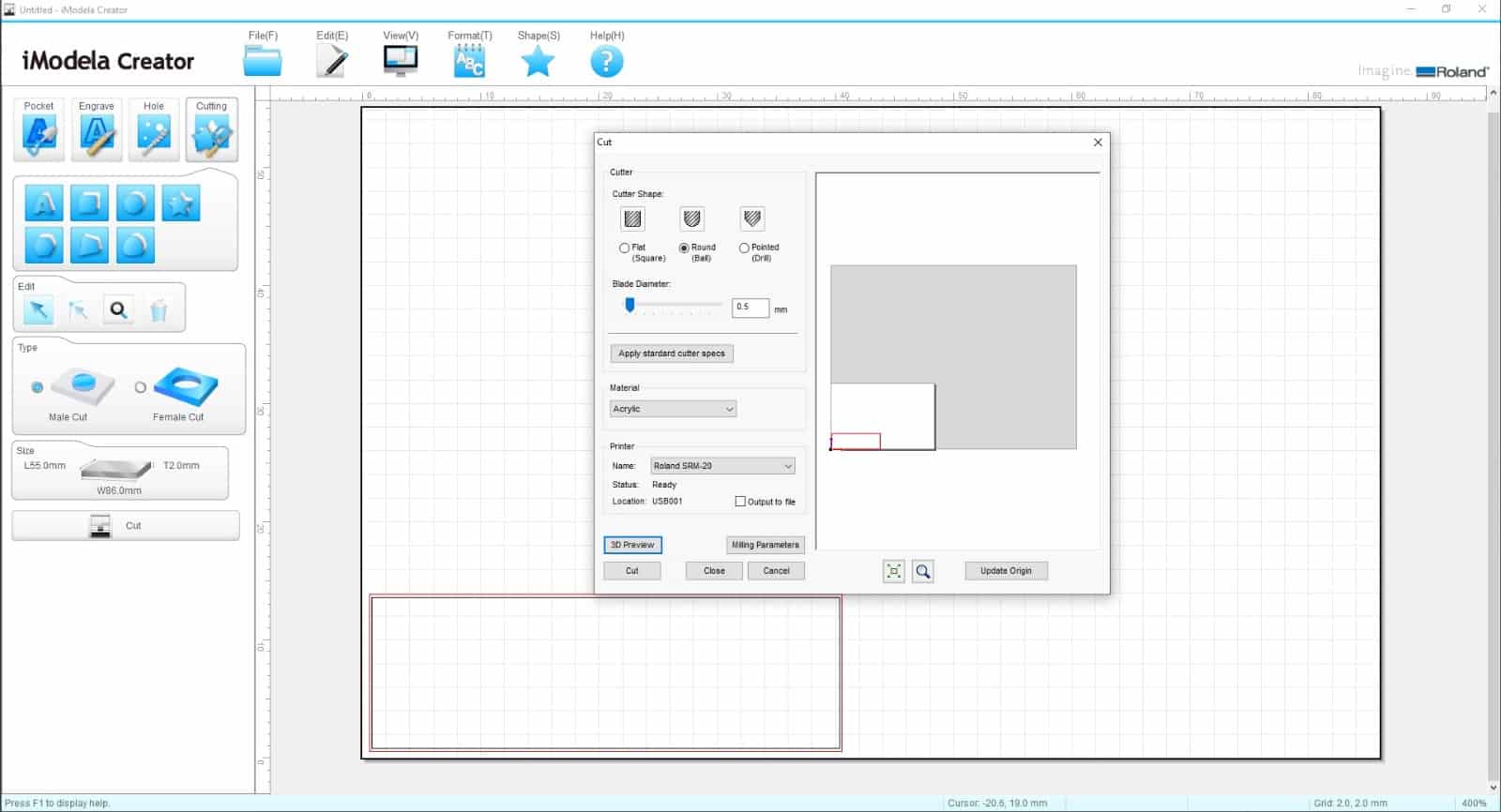
Generate Gerber files from the PCB design and send them to a manufacturer for production. Alternatively, use in-house PCB manufacturing equipment if available. /
Collect all the necessary components as per the schematic and PCB layout. Solder the components into their respective locations on the board. Ensure solid connections and avoid short circuits.
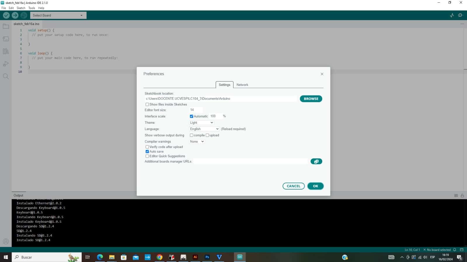
Use a suitable programmer to upload the firmware to the microcontroller. Make sure that the firmware includes the code necessary for the previously defined functions.

Perform basic tests to verify the functionality of individual components, such as LEDs, buttons, and sensors. Use measuring instruments (multimeter, oscilloscope) as necessary.
Connect external peripherals, such as sensors or communication devices, to ensure interoperability and test the board's ability to interact with other elements of the system.
Identify and correct possible problems or errors in the design and functionality of the board. Optimize the firmware code and adjust the settings as necessary.
- Conduct more extensive testing to evaluate the overall performance of the board under different conditions and expected usage scenarios.

- Create detailed documentation that includes the schematic, PCB layout, firmware source code and any other relevant information for future development or maintenance.
- If the development board is successful, it can proceed to mass production by adjusting the manufacturing process according to volume needs and requirements.