Week 8 Assignment
ELECTRONICS DESIGN
This week the individual assignment is to design and fabricate our own PCB (Printed Circuit Board), while our group's task revolves around collaboratively testing various electronic testing equipment. It's an exciting opportunity to apply my skills in PCB design and fabrication while also contributing to the group effort in ensuring the efficiency and accuracy of our testing instruments
Group Assignment Week 8
 Group Assignment
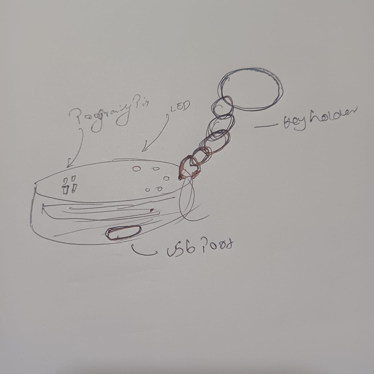
KEYCHAIN DEVLOPMENT BOARD
"Keychain Development Board" - This is my brainchild, my vision to create a versatile and compact tool for electronic prototyping. Picture this: a tiny, lightweight board that fits snugly on your keychain, ready to unleash your creativity anytime, anywhere. With this innovative device, you can bring your electronics projects to life on the fly.
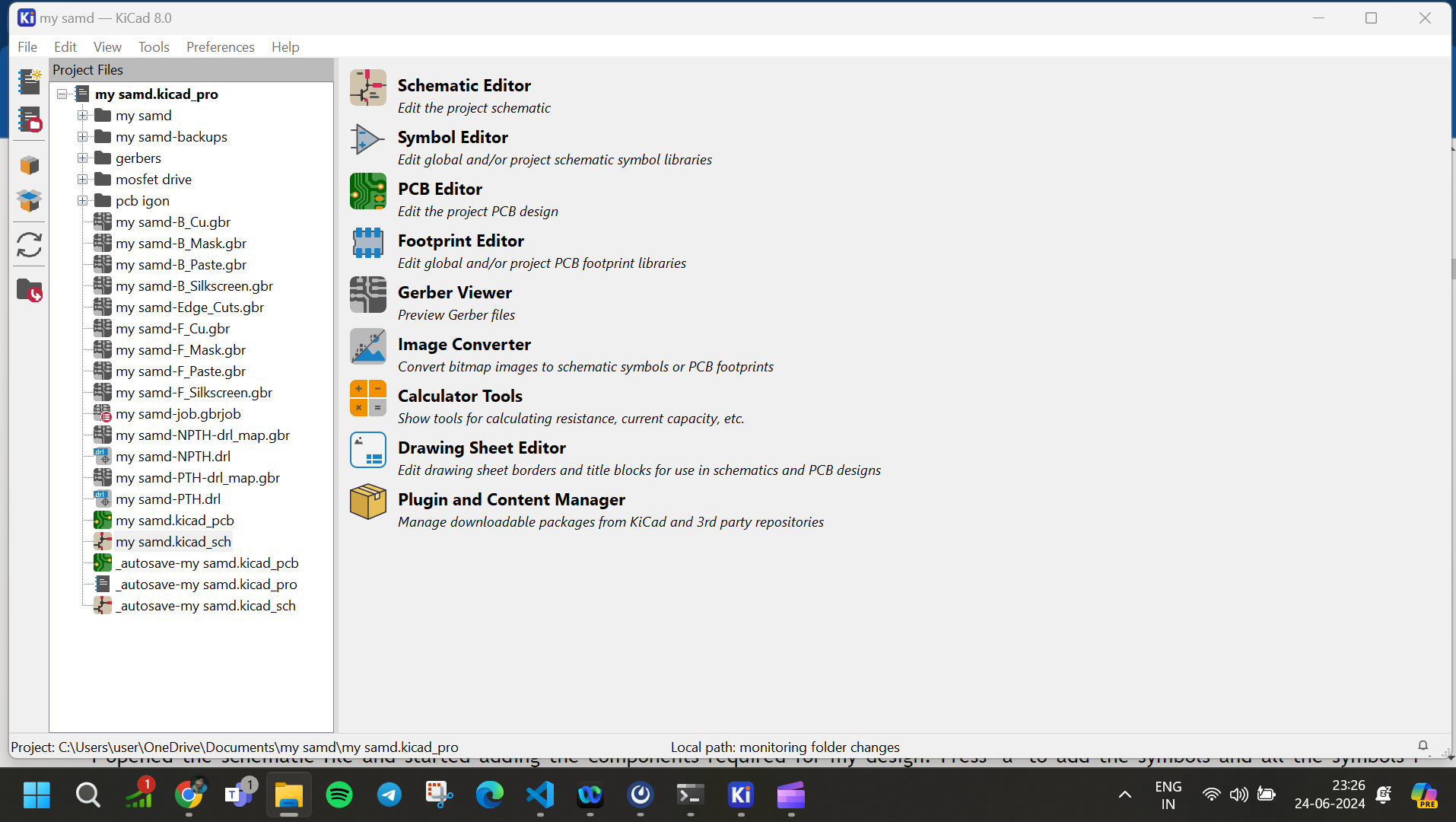
KiCad
KiCad is an open-source Electronic Design Automation (EDA) software that allows users to design electronic circuit schematics and convert them into PCB layouts. You can download KiCad by clicking here.
Fab Academy provides its own library of symbols and footprints for KiCad. I downloaded the .zip file from the following link:
https://gitlab.fabcloud.org/pub/libraries/electronics/kicad
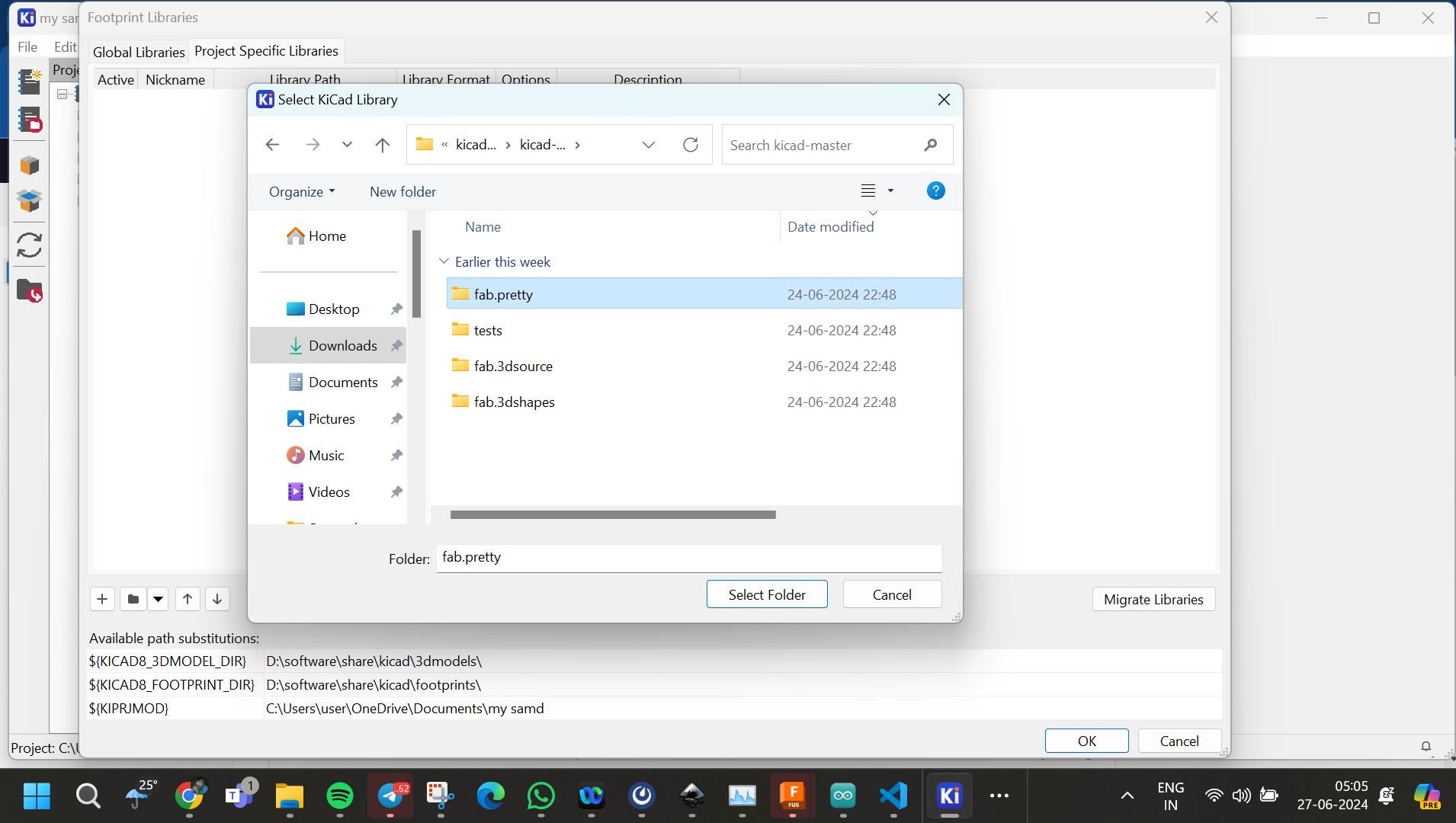
Adding Libraries to KiCad
To add the symbols file in KiCad, follow these steps:
- Open KiCad
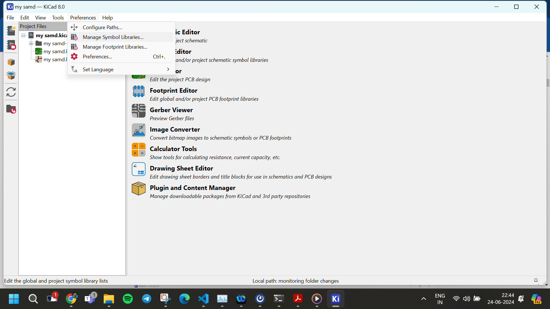
- Navigate to Preferences > Manage Symbol Libraries > Add file
-
add the symbol files and click ok
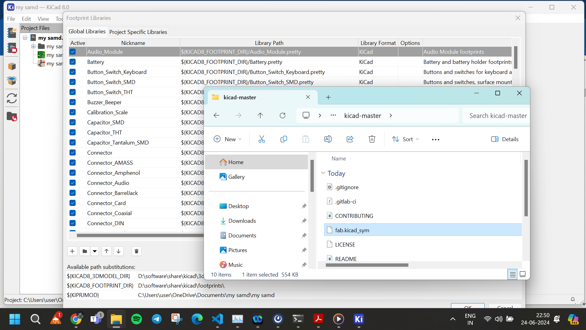
- Ensure all components from the schematic have corresponding footprints assigned in the PCB editor.
- Go to Preferences > Footprint Libraries Manager to verify and add footprints if necessary.
- Select and assign footprints to components by placing them on the PCB layout.
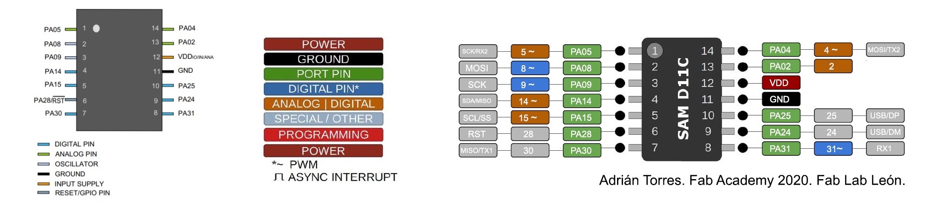
SAMD11C Microcontroller
Overview
The SAMD11C is a microcontroller from Microchip's SAM D11 series, designed for small, low-power applications that require high performance. It features a 32-bit ARM Cortex-M0+ processor core running at up to 48 MHz, offering a good balance of power efficiency and processing capability.
Pinout
The SAMD11C microcontroller typically comes in a compact package with a variety of pins for different functionalities:
- GPIO (General Purpose I/O): These pins can be configured as digital inputs or outputs for interfacing with external devices.
- Analog Inputs: Some pins support analog-to-digital conversion (ADC), allowing measurement of analog signals.
- Serial Communication: UART, SPI, and I2C interfaces facilitate communication with other devices such as sensors and peripherals.
- Timers and PWM: Built-in timers and PWM (Pulse Width Modulation) outputs enable precise timing and control of signals.
- Power Management: Pins for power supply and management, including voltage regulators and sleep modes for optimizing power consumption.
- Special Functions: Some pins may have special functions such as interrupts, debugging, or specific peripheral connections.
Features
The SAMD11C microcontroller offers a range of features suitable for various embedded applications:
- ARM Cortex-M0+ Processor: 32-bit RISC architecture with efficient performance and low power consumption.
- Memory: Up to 16 KB of Flash memory for program storage and up to 4 KB of SRAM for data storage.
- Peripherals: Includes UART, SPI, I2C, ADC, DAC, PWM, and GPIO for versatile connectivity and control.
- Low Power: Power-saving modes and features to minimize energy consumption, suitable for battery-powered applications.
- Security Features: Hardware-based security features for protecting data and code integrity.
- Integrated Development Environment (IDE) Support: Compatible with industry-standard development tools like Atmel Studio and Arduino IDE.
 samd11 datasheet
OTHER COMPONENTS
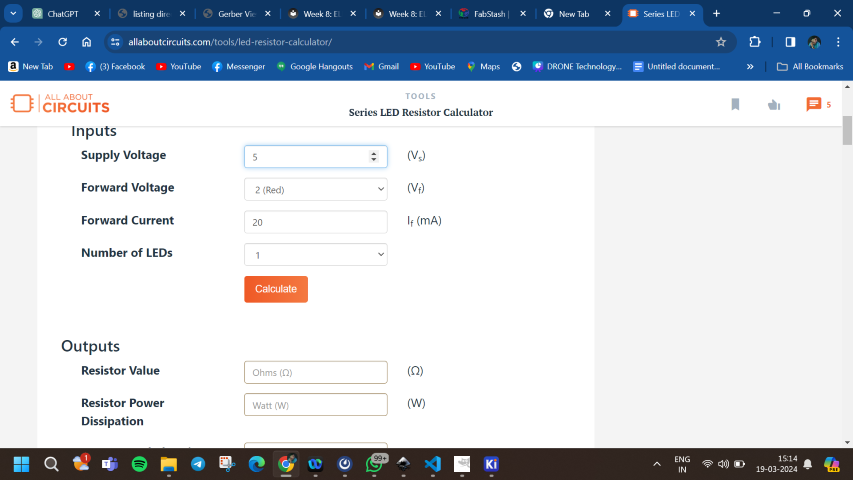
Starting with the essentials like LEDs, switches, and the WS2812 LED, I also incorporated additional output device pinouts and power rails and switch as a input device . To guarantee optimal performance, I integrated a voltage regulator circuit into the schematic. This regulator would stabilize the input voltage, ensuring a consistent 3.3 volts supply to all components. This step is crucial for enhancing the reliability and overall performance of the development board. Moreover, I utilized an online resistor calculator to determine the appropriate resistor values for the LEDs, ensuring they receive the correct current for optimal brightness while preventing damage. With these crucial components and calculations in place, my schematic is taking shape, laying the foundation for the subsequent stages of PCB layout design and fabrication.
Schematic drawing in KiCad
Step-by-Step Guide
1. Creating a New Project:
- Open KiCad and create a new project or open an existing one where you want to add your schematic.
2. Opening Schematic Editor (Eeschema):
- From the KiCad main window, click on the "Schematic Layout Editor" (Eeschema) icon.
- This opens the schematic editor where you will create your schematic.
3. Adding Components:
- Click on the "Place" menu or press "a" on your keyboard to access the component libraries.
- Choose the library that contains the component you need (e.g., "fab" for Fab Academy symbols).
- Click on the component you want to add, then place it on the schematic editor window by clicking on the desired location.
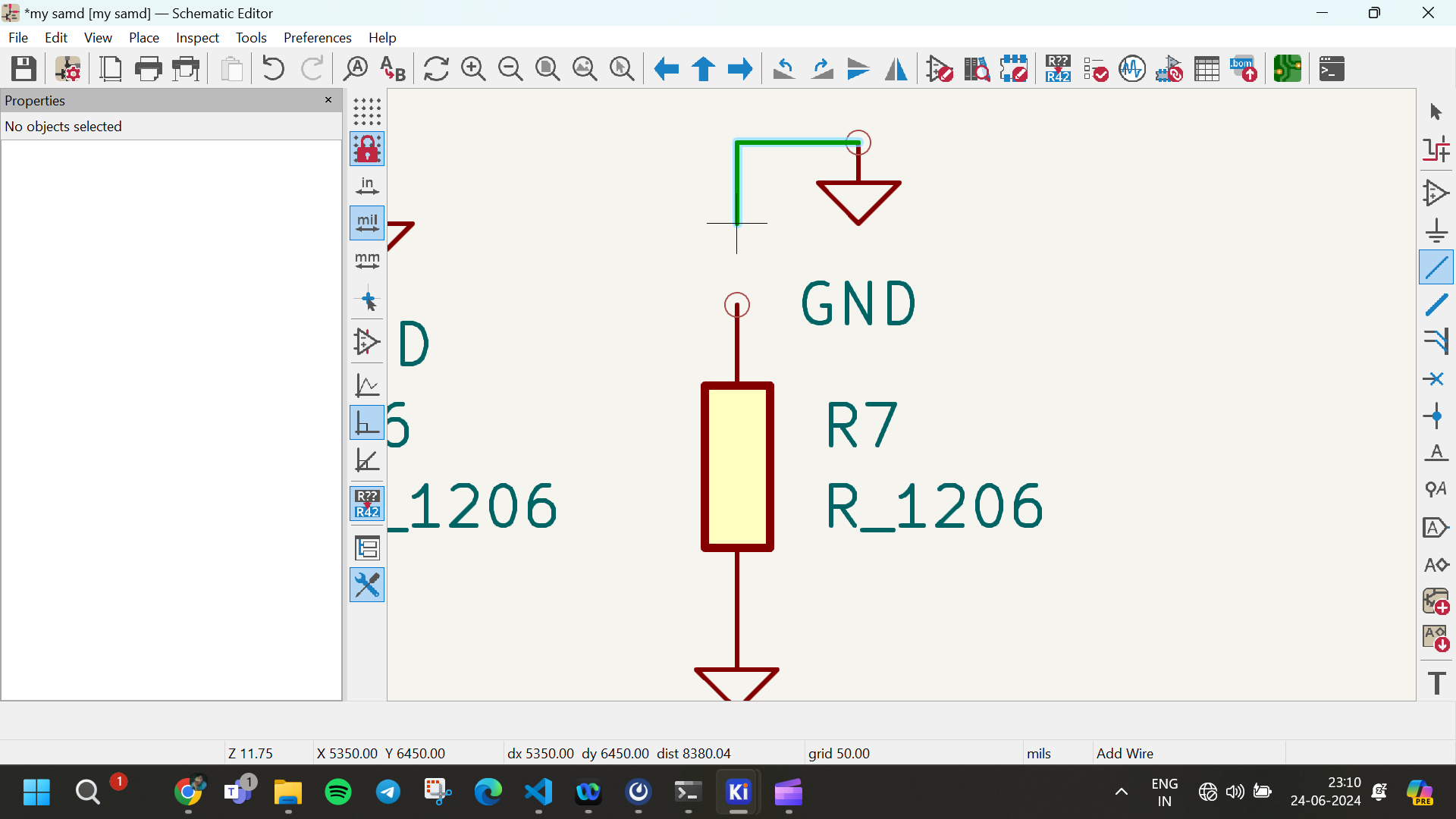
4. Wiring Components:
- Use the "Place Wire" tool (shortcut: "w") to connect the pins of components.
- Click on the pin of one component, then click on the pin of another component to create a wire connection between them.
- Continue wiring all necessary connections according to your circuit design.
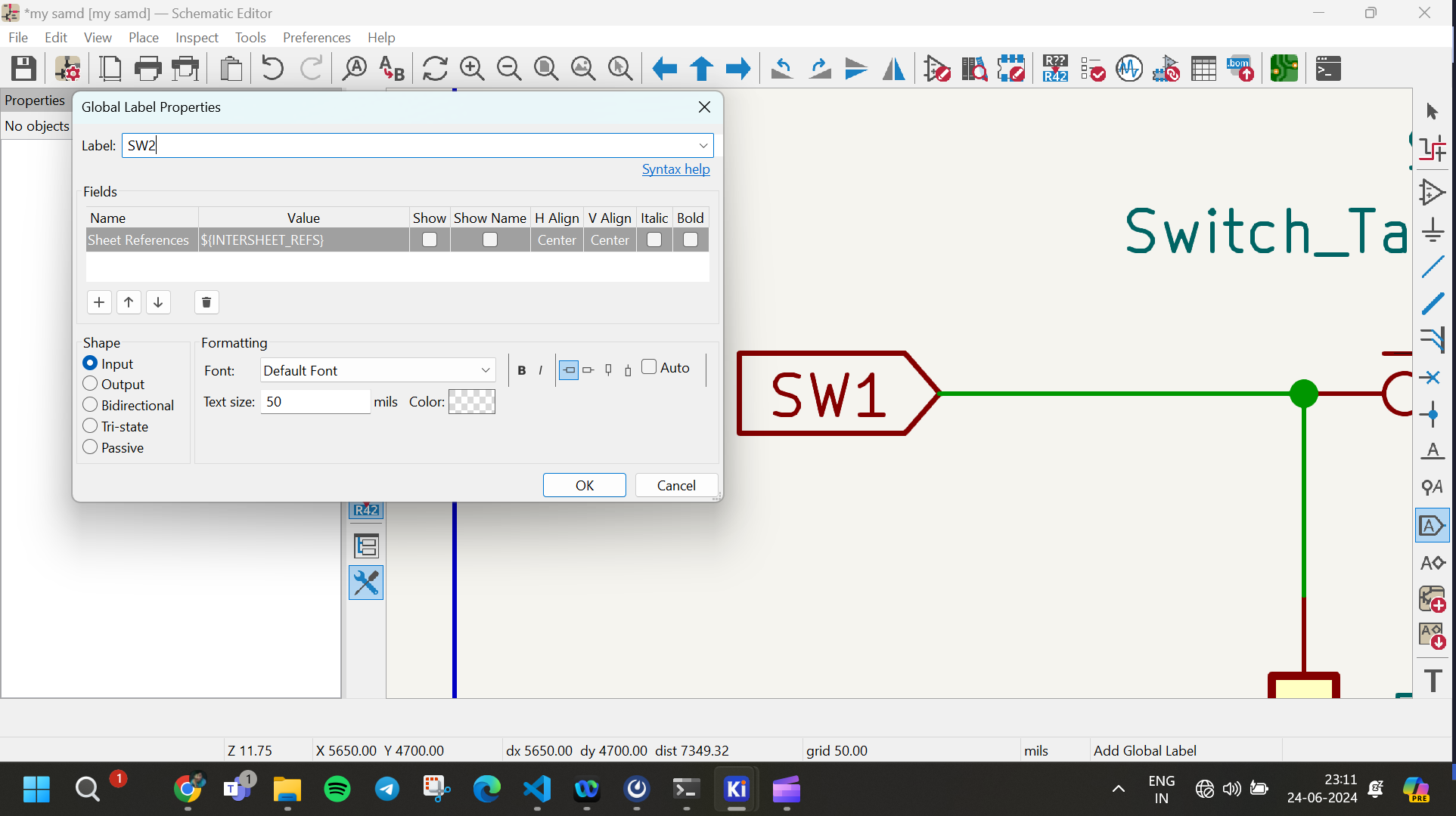
5. Adding Labels and Global Labels:
- Labels (shortcut: "l") are used to name nodes or nets (connections) in your schematic.
- Global labels (shortcut: "g") are used for signals that need to be connected across different sheets in hierarchical designs.
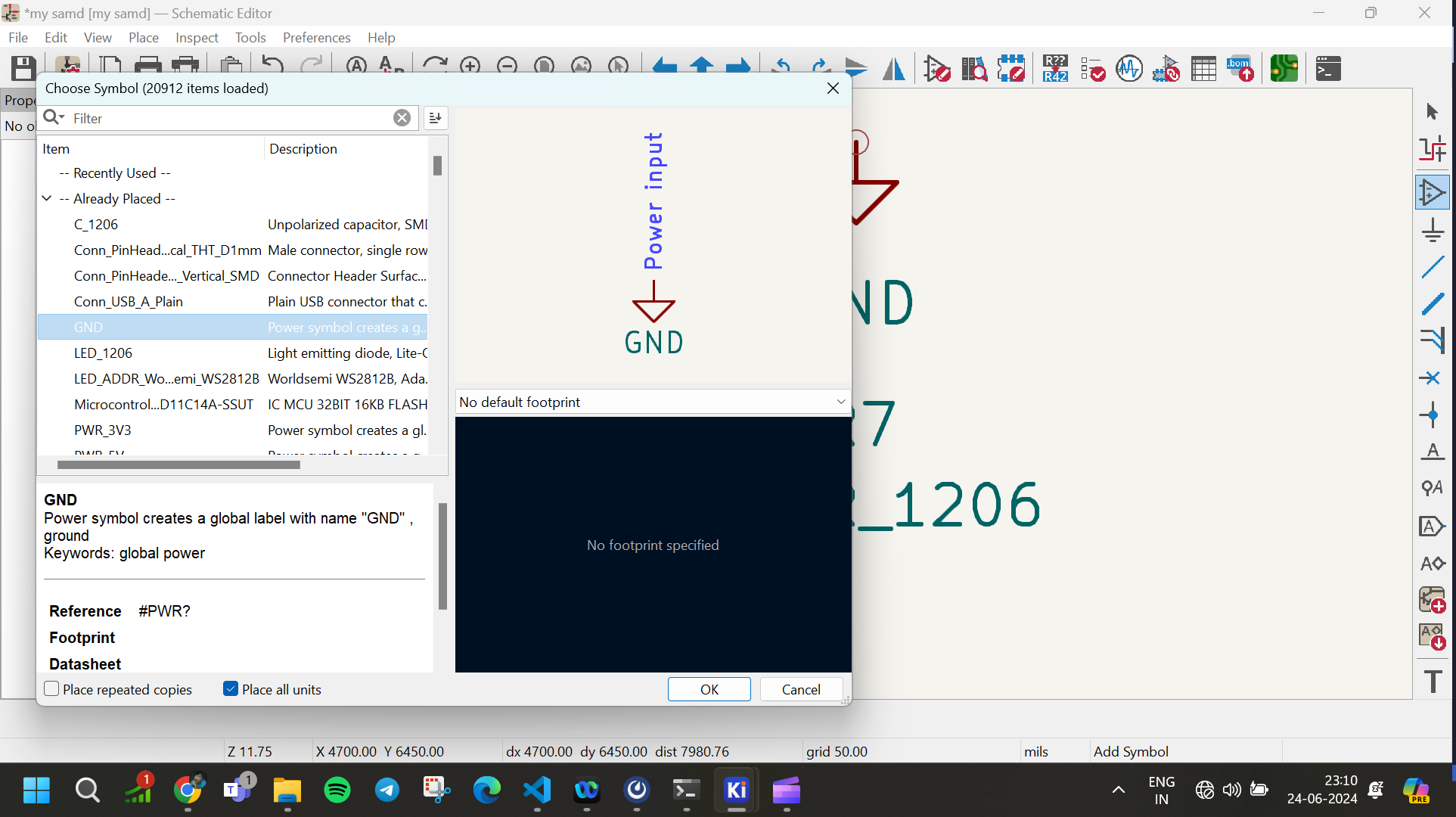
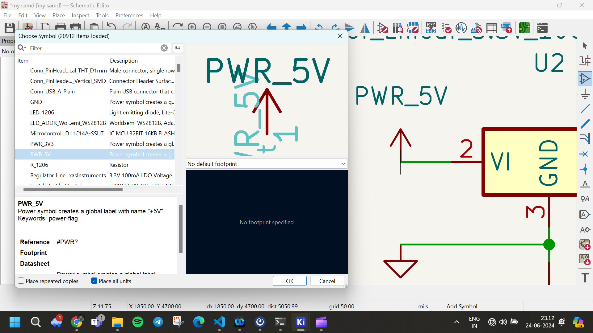
6. Adding Power Symbols and Ports:
- Place power symbols (like VCC, GND) from the component libraries where power connections are needed.
- Ports (shortcut: "p") are used to create connections that can be referenced from other sheets in hierarchical designs.
7. Annotating Components:
- After placing all components, annotate them to assign unique reference designators (like R1, C2, U1, etc.) automatically.
- Go to "Tools" > "Annotate Schematic" and follow the prompts.
9. Saving Your Schematic:
- Save your schematic regularly using "File" > "Save" or "Save As..." to ensure you don’t lose your work.
12. Exporting:
- Finally, export your schematic in a format suitable for PCB layout (if needed) or for sharing with others.
Additional Tips:
- Keyboard Shortcuts: Learn and use keyboard shortcuts for faster workflow (e.g., "a" for placing components, "w" for wiring).
- Component Libraries: Utilize custom or third-party component libraries if KiCad’s default libraries do not have the components you need.
- Documentation: Document your schematic thoroughly with clear labels and notes for better understanding by yourself and others.
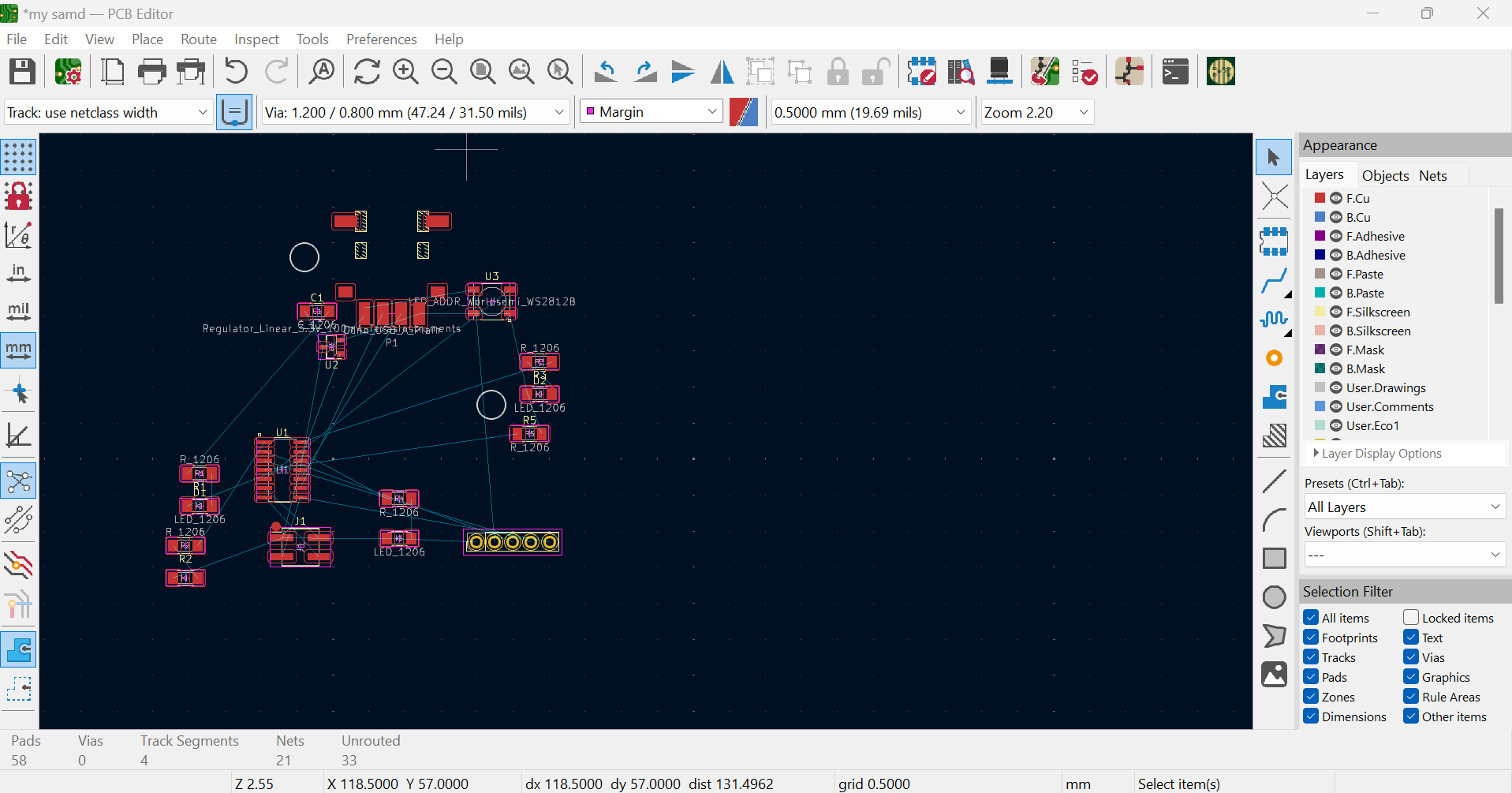
Converting Schematic to PCB and PCB Routing in KiCad
1. Converting Schematic to PCB:
Opening PCB Layout Editor:
- From KiCad, switch to the PCB Layout Editor (Pcbnew) by clicking on the icon or navigating through the menu.
- Example: Tools > PCB Layout Editor (Pcbnew).
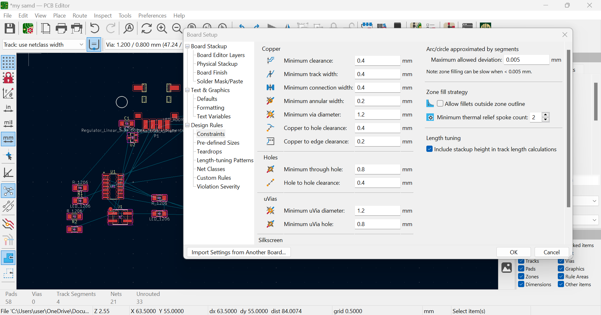
2. Setting Design Rules (DRC):
Configuring Trace Width and Clearance:
- Set trace width and clearance rules to ensure proper signal integrity and manufacturing requirements.
- Go to Boardsetup>constrains>Design Rules and configure:
- Trace Width: Typically set to 0.4 mm.
- Clearance: Minimum spacing between traces, usually set to 0.4 mm.
Setting Via Parameters:
- Configure via parameters including via hole size and via pad size.
- Go to Design Rules > Design Rules Checker > Global Design Rules > Via Style:
- Minimum Via Hole Size: Set to 0.8 mm.
- Minimum Via Pad Size: Set to 1.4 mm.
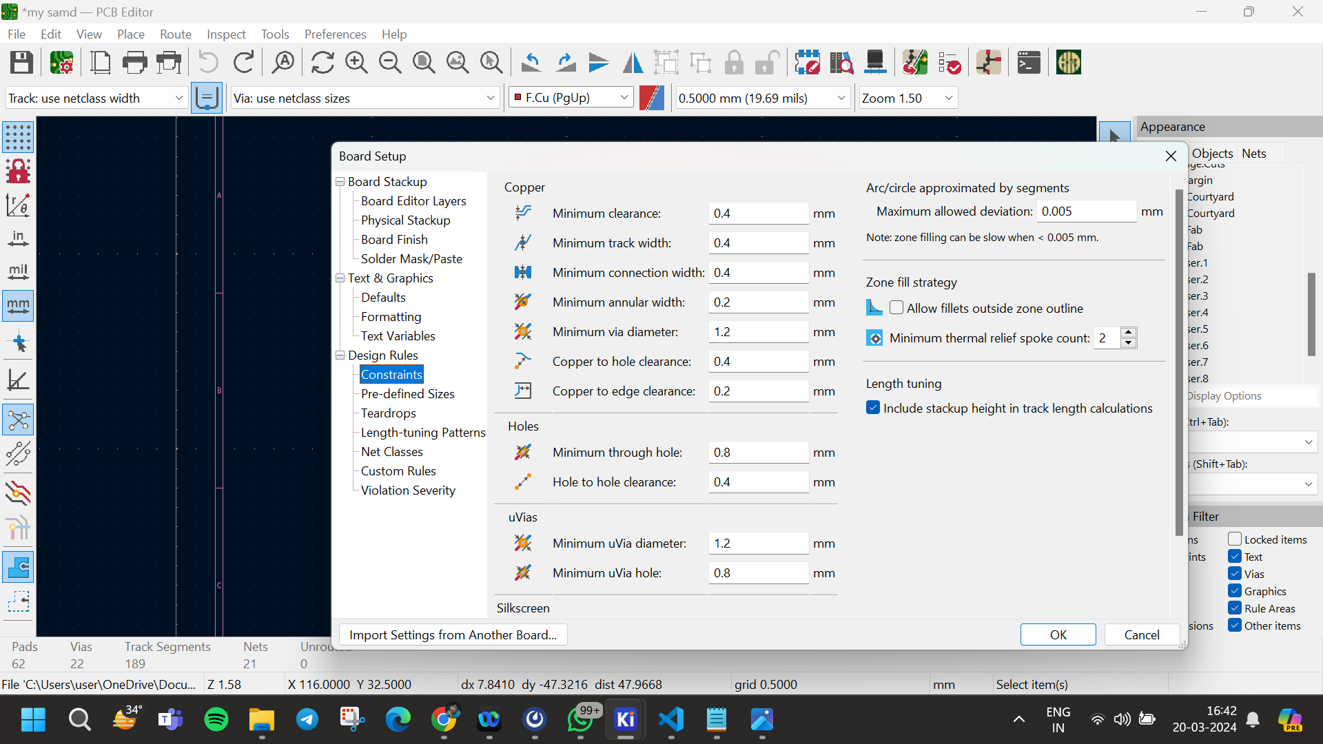
- I have selected the values based on the assigment that was done on the elctronics production week and set the values accordingly to meet the milling machines totalrances
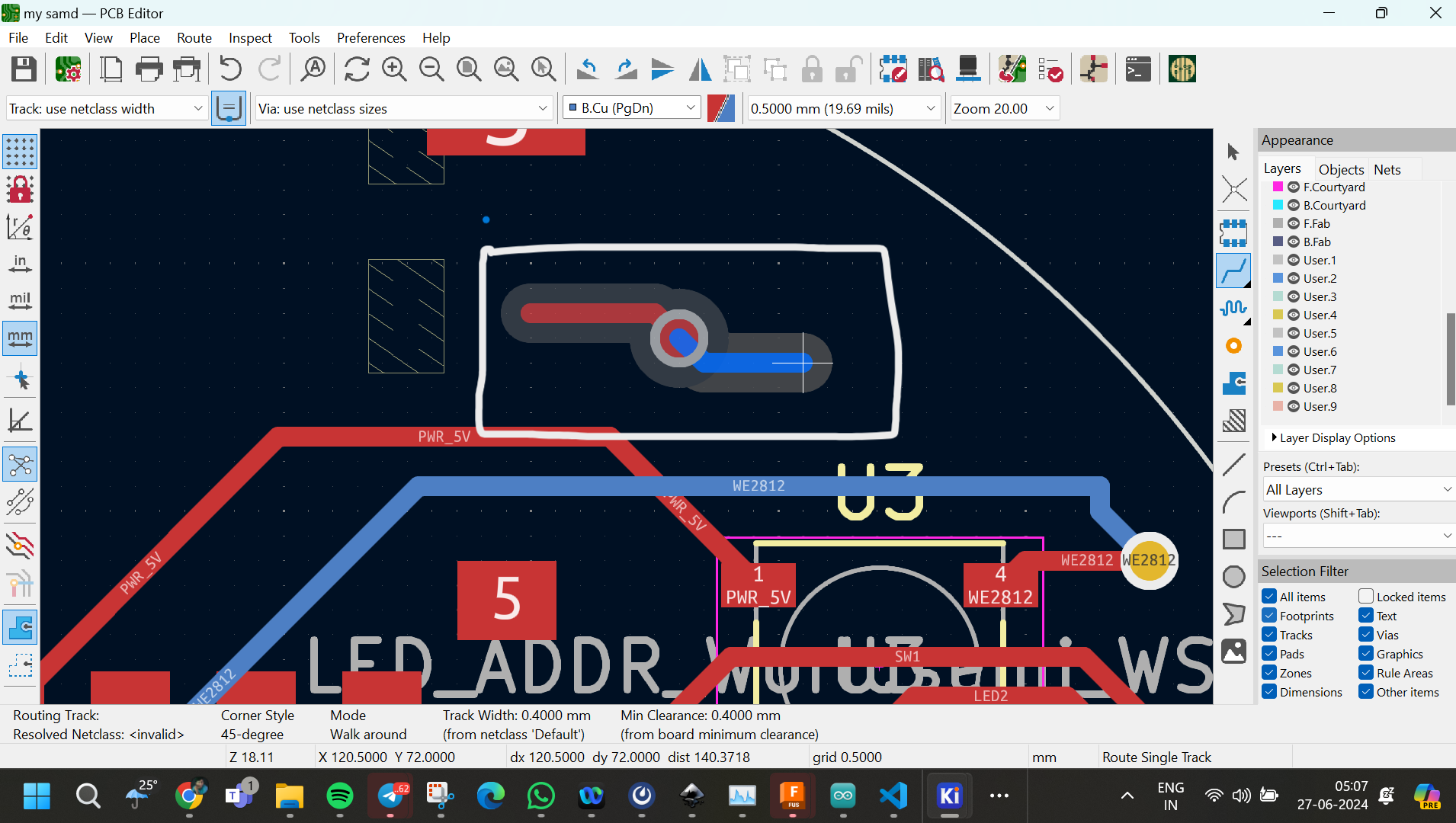
3. PCB Routing Process:
Routing Traces:
- Start routing traces to connect components according to your schematic.
- Use the Route Tracks tool to draw traces between pads, adhering to DRC settings.
- Ensure to minimize trace crossings and maintain proper clearance.
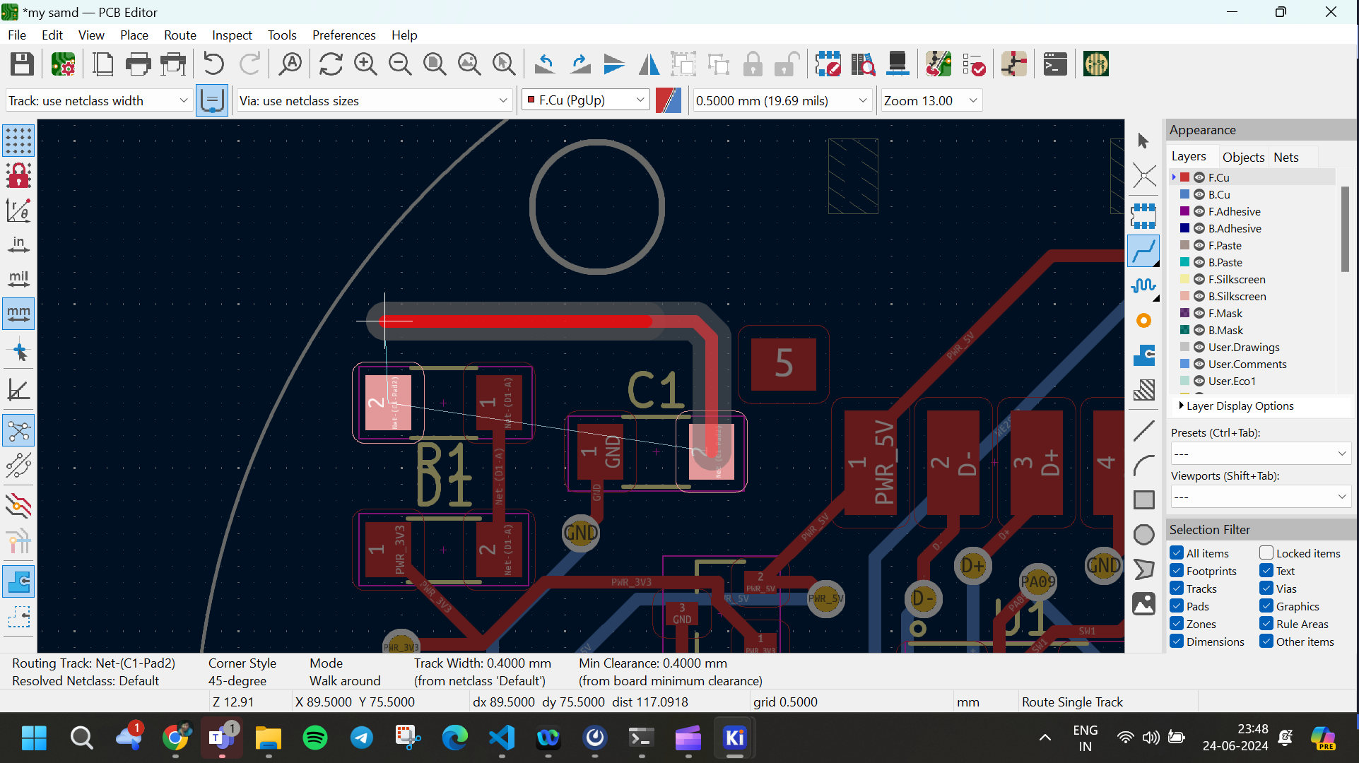
Routing Bottom layer :
- Start routing traces as normal to switch from top copper layer to bottom click on V it will add VIA and switch to bottom layer and traces can be complete it in bottom layer as well
- this used Ensure trace crossings and make the size of the pcb compact
- Once teh routing is finished the drc checking is done to ensure the routing haven't breached any design parameter,in any it is acknowledge and action taken to ensure it has been clered
- Go to Inspect>Design Ruleschecker and click on run DRC
4. Exporting to Gerber Files:
Preparing for Manufacturing:
- Before manufacturing, export your PCB design to Gerber files, the standard format used by PCB manufacturers.
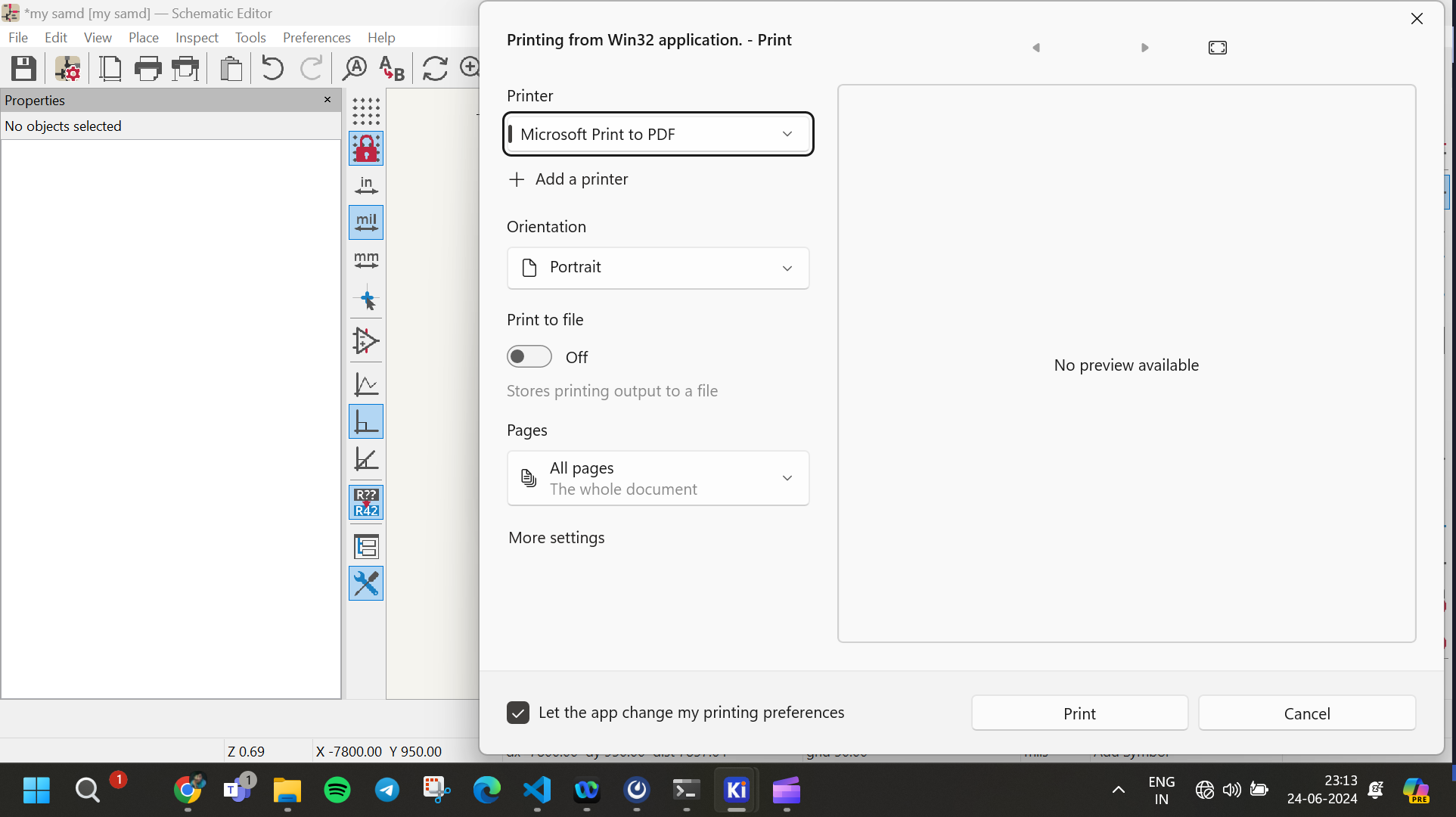
- Go to File > Plot to open the plot dialog in KiCad.
- Configure plot settings such as layers to plot, output directory, and file format (Gerber).
- Click on Plot to generate Gerber files.
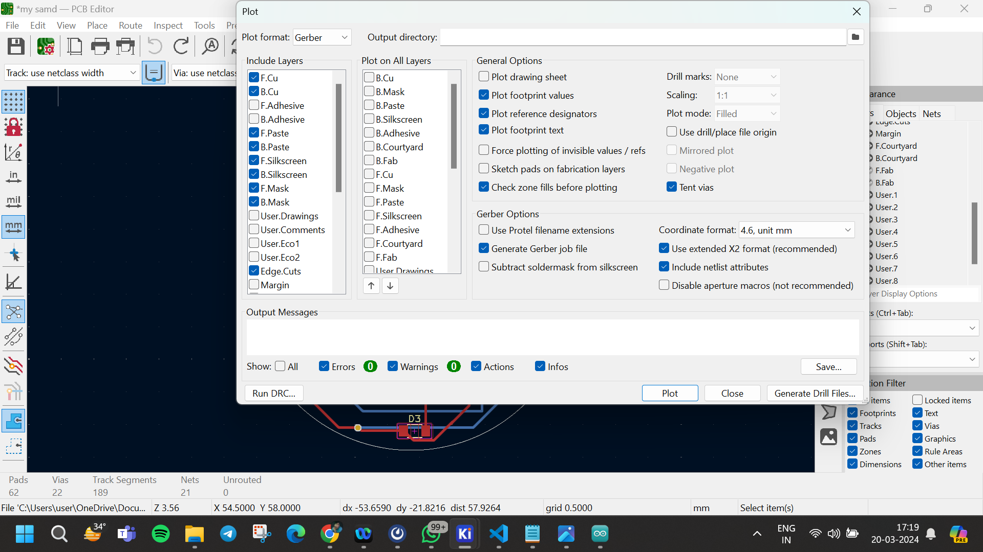
Final Checks and Documentation:
- Review the generated Gerber files using a Gerber viewer to ensure all layers and details are correct.
- Generate other necessary manufacturing files (like drill files) if required.
- Document your PCB design thoroughly with design notes and annotations for manufacturing and assembly.
By following these steps and configuring settings as described, you can efficiently convert your schematic to a PCB layout and prepare it for manufacturing using KiCad.