as neil said this week kicked of to be boring, there was not much things to do but i am planing to do some things while building the pcb i have bit of expeince in this domin so i will take take the time to also help my fellow accadamy mates as well...
this perticulaer board that we are trying to fabricate is the brain child of Quentin Bolsée and redesigned by Adrián Torres. this board runns a seeed studio xiao as the mcu and the devleopment board is basicaly intagrated to the pcb like an expansion board expanding ou the swd,uart adapters and a power brake out as well, this is an open board avilable for anyone to make and test it's capacities
This perticuler machine was manufactured to be used to make lost wax casting moulds for jewllers but we are now using it as a pcb milling machine, this machine carries the following spscifications
XY table size - 220 (X) x 160 (Y) mm ( 8-5/8 x 6-1/4 in.)
Max. operation area - 203.2 (X) x 152.4 (Y) x 60.5 (Z) mm (8 (X) x 6 (Y) x 2-3/8 (Z) in. )
Weight - 1000 g (2.2 lb.)
PCB MILLING
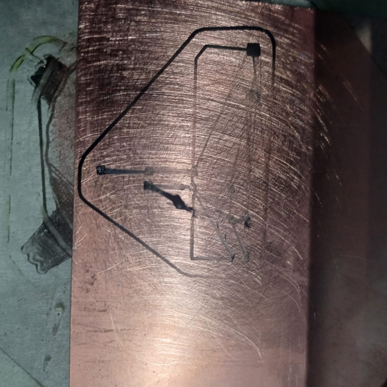
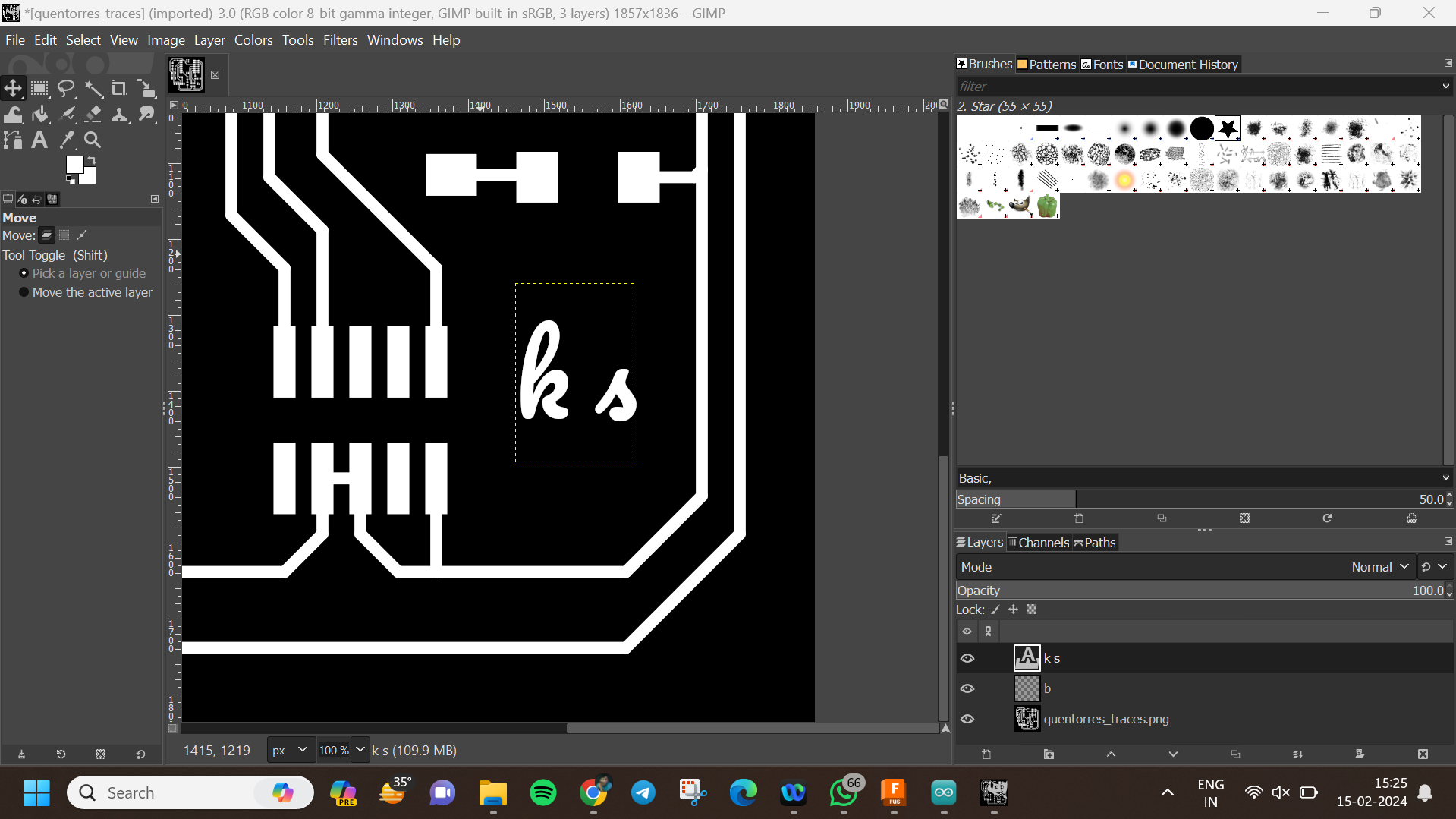
then we procced to do some ctting with that for that we downloded the png on the quendoress devlopment board into our local machine
then i opend the file in gimp for a quick view and edit ing it and adding my initails to the board, i used the bresh tool to remove the original logo then aded my initails using the text tool and exported it as png and saved it in local machine
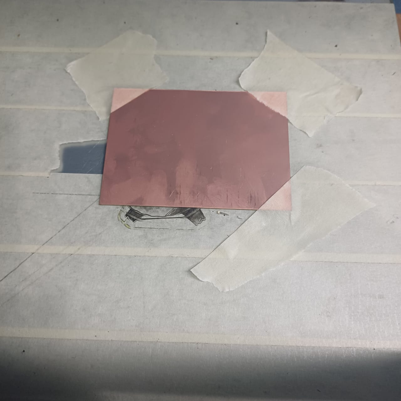
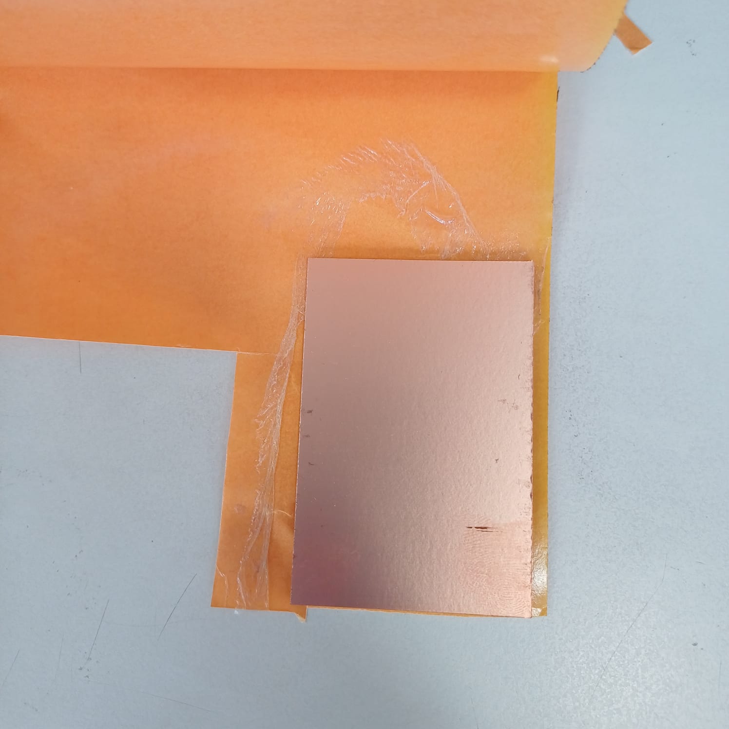
So first i went and took a FR1 copper clad and stuck it to the bed using the thin double sided tape
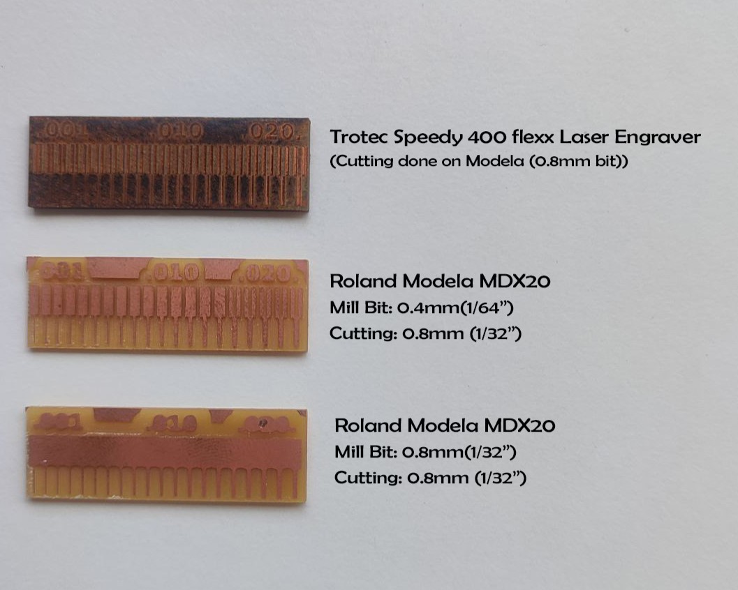
Milling PCB Traces and Drilling Holes using Roland Modela MDX-20 and MODs
Milling PCB Traces
Prepare Trace File
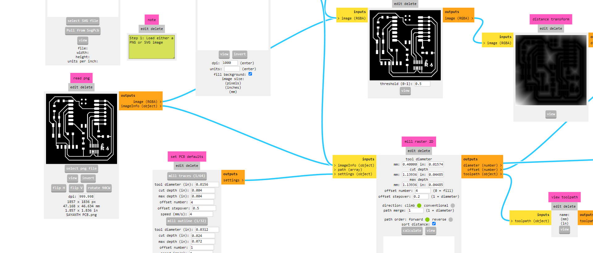
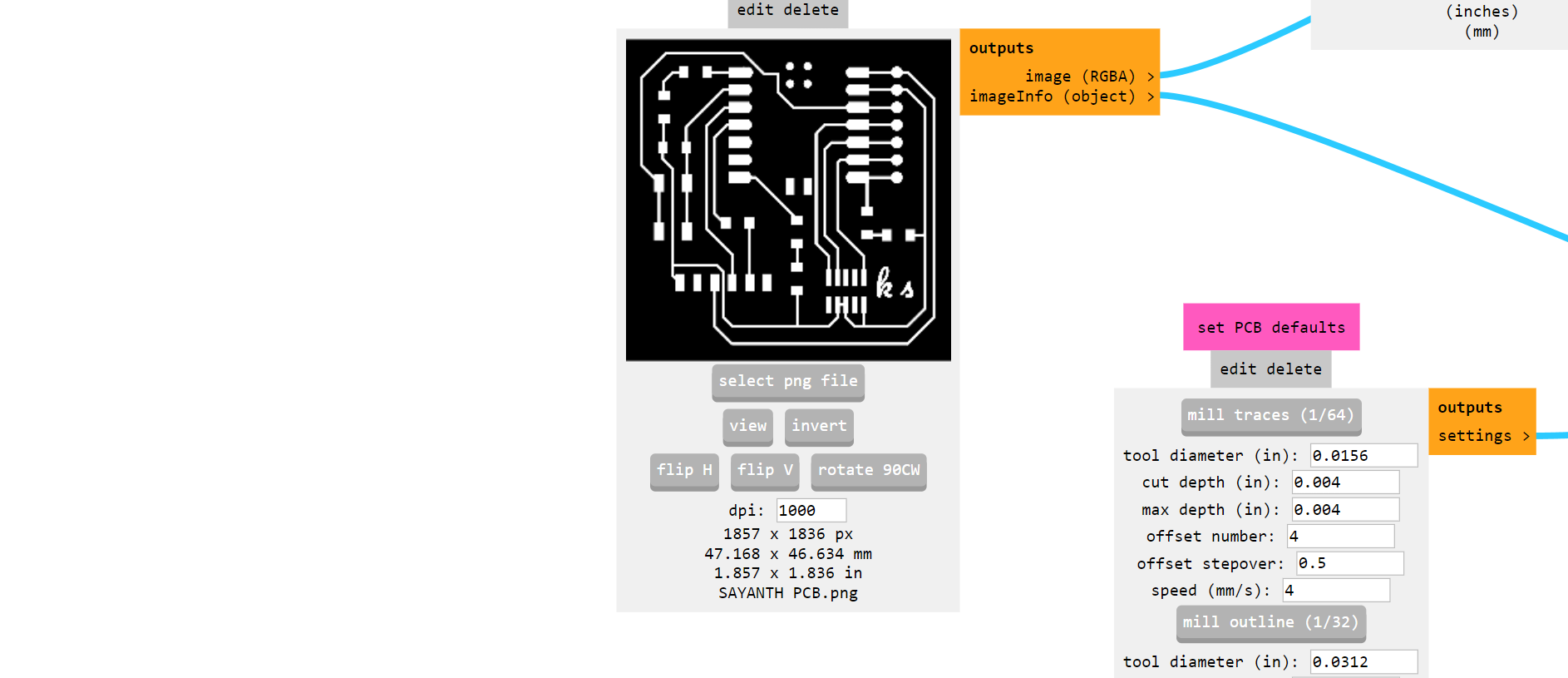
Ensure your trace file is in a compatible format (.png).
Black areas indicate copper to be milled away, white areas remain as traces.
Launch MODs
Open MODs in your web browser.
Select the Roland MDX-20 milling machine configuration for PCB milling.
Import Trace File
Click on "Open Server Program" and select "Roland MDX-20 PCB".
Import your trace file by selecting the "Read PNG" module and loading your file.
Set DPI
In the "Read PNG" module, set the DPI (dots per inch) to 1000.
Choose Milling Bit
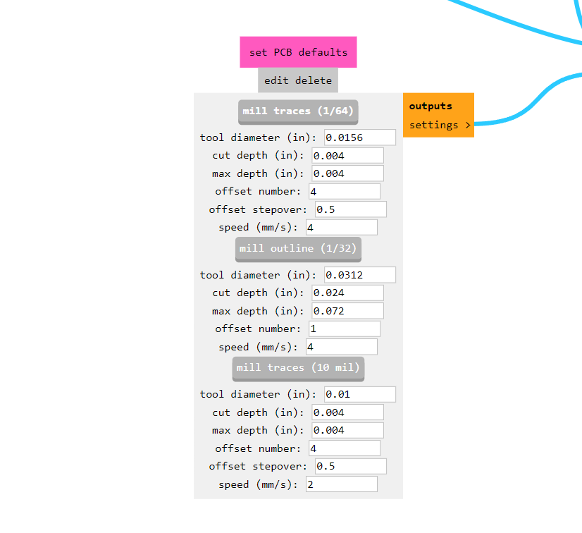
Select a 0.4mm (1/64") milling bit for traces.
In MODs, set the tool diameter accordingly in the settings.
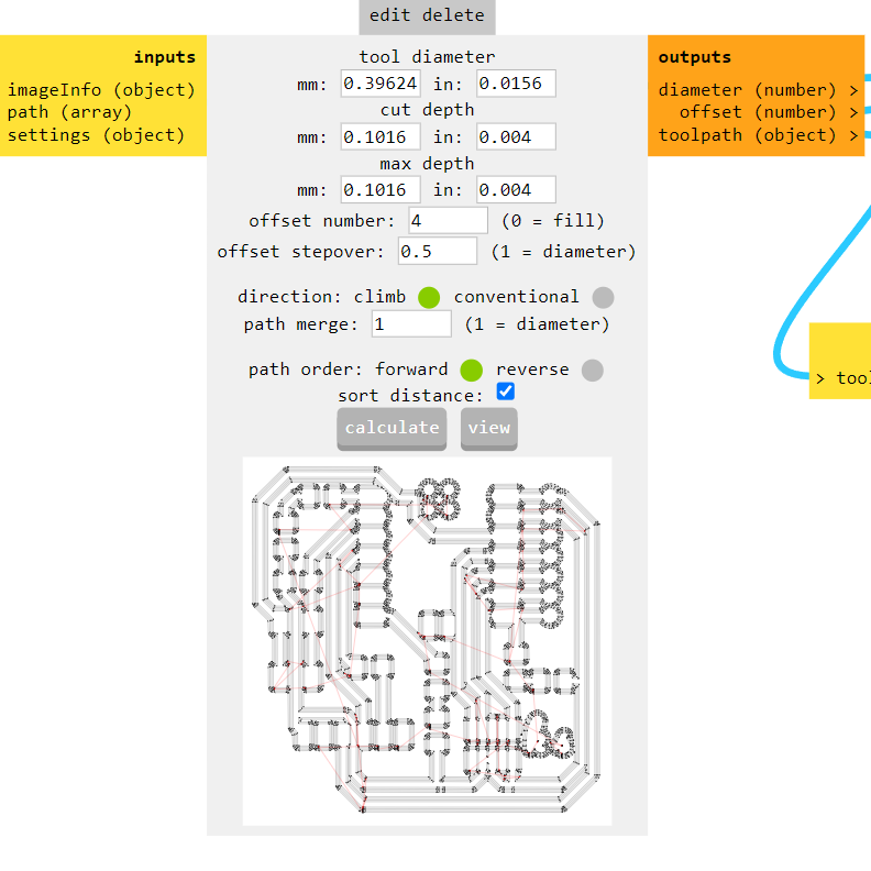
Calculate Toolpath
Use the "Mill Traces" module.
Click on "Calculate" to generate the toolpath.
View the path by clicking on the "View" button to ensure correctness.
Prepare the Machine
Switch on the Roland MDX-20.
Press the "View" button on the machine control panel to move the module to its home position.
Install the 0.4mm bit using an Allen key.
Secure the FR-1 PCB material onto the machine bed using double-sided sticky tape.
Ensure the machine bed is clean from any sticky residue.
Set Origin Position
In MODs, adjust the origin position to your desired starting point.
Click "Move to Origin" to position the bit correctly.
Lower the Bit
Use the down button on the machine control panel to gently lower the bit until it touches the PCB surface.
Start Milling
In MODs, click on "Send File" to start the milling process.
Monitor the process to ensure it proceeds correctly.
Drilling Holes and Cutting Out the PCB
Import Drill and Cut Files
Open MODs again and import the provided .png files for drilling and cutting.
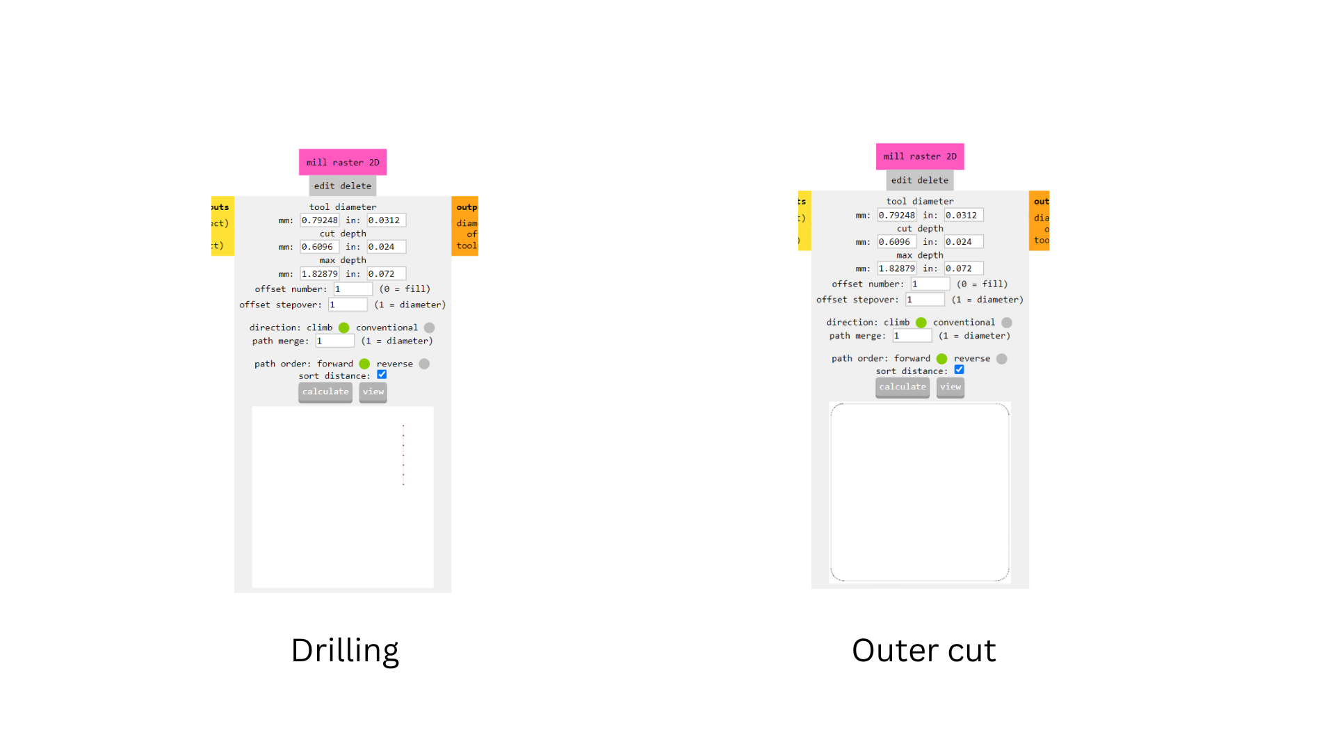
Change Milling Bit
Replace the 0.4mm bit with a 0.8mm (1/32") bit suitable for drilling and cutting.
Use an Allen key to securely fasten the new bit in the collet chuck.
Calculate Toolpath for Drilling and Cutting
In MODs, load the .png files for the drilling and cutting paths.
Adjust settings as necessary (e.g., tool diameter, depth of cut).
Calculate the toolpath for each operation and view to verify.
Set Origin Position for Drilling/Cutting
Set the origin position again if necessary.
Use the "Move to Origin" feature in MODs.
Lower the Bit for Drilling/Cutting
Gently lower the bit using the down button until it touches the PCB.
Start Drilling/Cutting
Click "Send File" in MODs to start the drilling process.
Once drilling is complete, repeat the process for cutting out the PCB
Ensure all operations are correctly performed by monitoring the machine.
Finishing Up
Power Down the Machine
Once all milling and drilling operations are complete, switch off the Roland MDX-20.
Carefully remove the PCB from the machine bed.
Clean Up
Remove any leftover tape and clean the machine bed.
Store the milling bits and tools properly.
Inspect the PCB
Check the milled PCB for any issues or incomplete cuts.
Clean the PCB surface if necessary.
This is a short clip of the milling opration
SOLDERING
Soldering is a fundamental technique used in electronics and metalwork to join two or more pieces of metal together by melting a filler metal, known as solder, into the joint. This process creates a strong and conductive bond between the components.
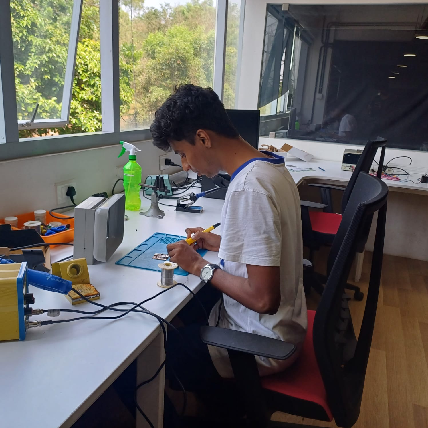
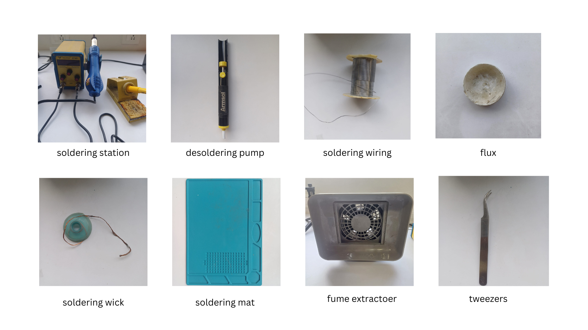
so these are some of the tools that i used to solder my board together
TIPS AND TRICKS TO SOLDERING
so i been soldering from a very young age and these are some of the things that i really love to share here that might help people who are getting into soldering
Proper Tip Maintenance: Keep your soldering iron tip clean and tinned. Wipe it on a damp sponge or brass wire cleaner regularly to remove any oxidation buildup
Use the Right Temperature: Different soldering tasks require different temperatures. Generally, for electronics work, temperatures between 300°C to 350°C (570°F to 660°F) are suitable
allways apply flex: don't hesitate to put bit of flex in joints it allways create a good joint but also make sure that you are not puuting to much it is allways a delicate balance
practice well: i started to practice with soldering idrrent alphabets using wire and soldering them together and also using dot board to solder random components together
PCB ASSEMBLY
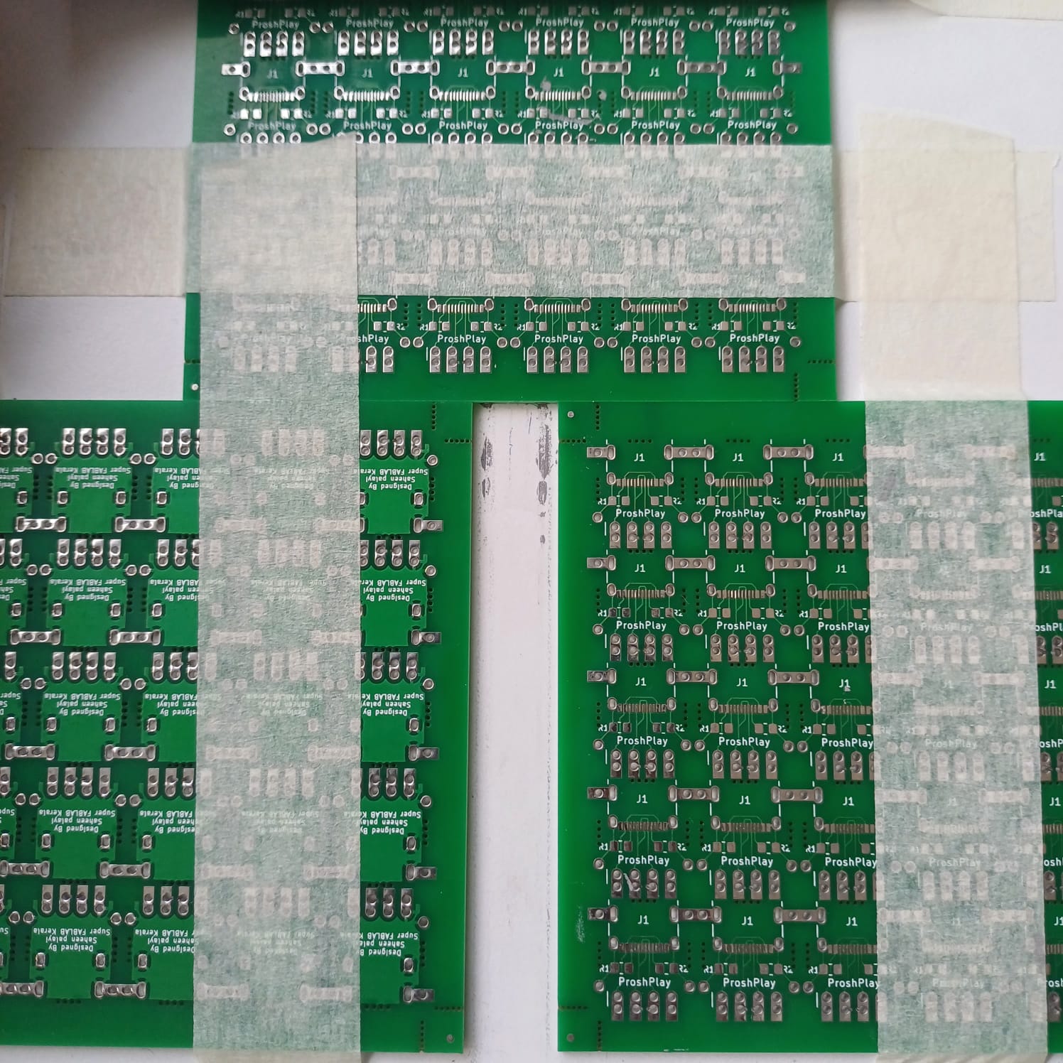
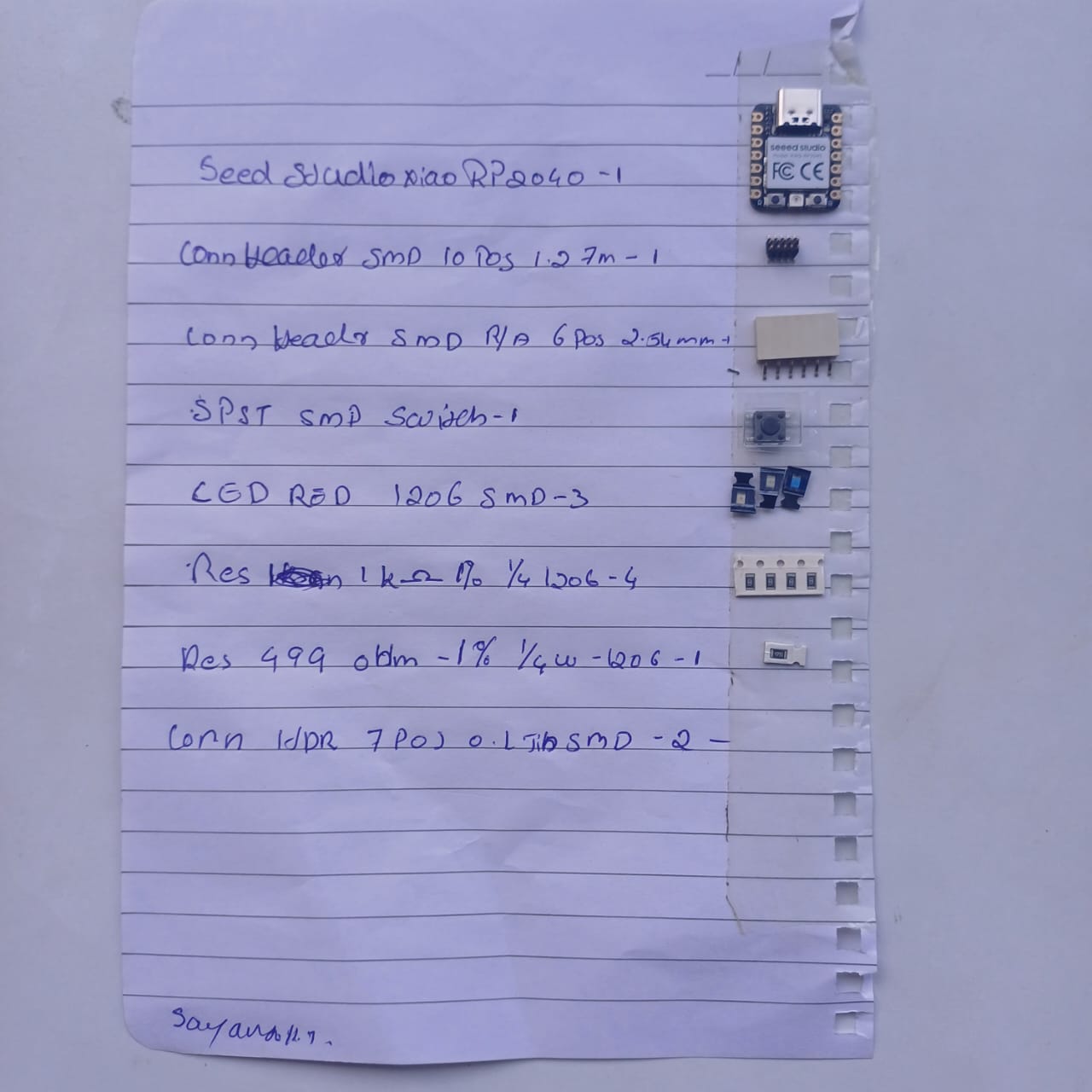
in order to start assembly of the pcb i prepared the BILL OF MATERILS and used the fab inventoery app of our local fablab to take the nessery componts and made a list and sticked it to that using a double sided tap
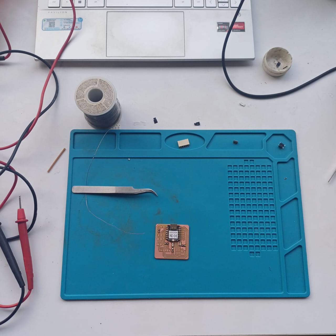
so as a person who is fairly experinced in soldering both through hole and smd componts it was a piece of cake for me i took up the pcb asssebly diagram from the quntars page and opend it in my laptop and revisted the compontes placement becuse the was no Silkscreen on the pcb it self
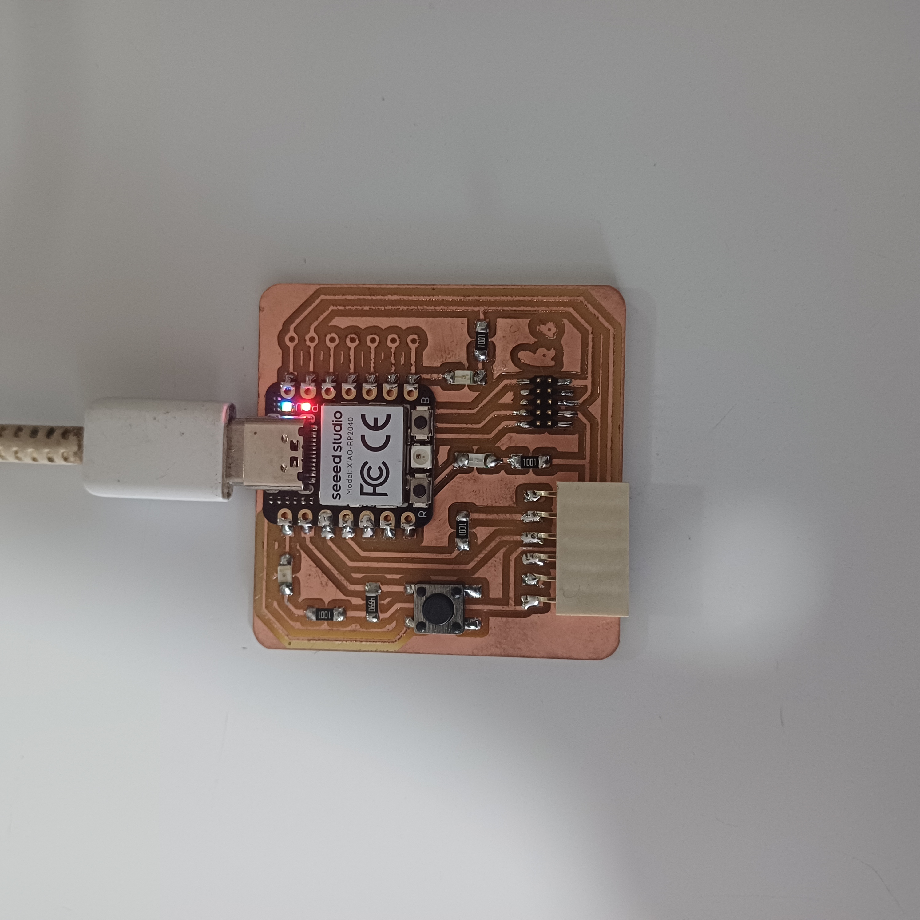
then i used the solderon soldering station and set the temprature to 350 degree and stared assebling the small par ts like the resiteres and leds first and then the xiao and tehn then the connecters
then i did a visuel inspection to ensure there are no physical short of the board and then proccede to clean the board using isopropyle solution and moved to proggram the board using arduino IDE
PROGRAMMING
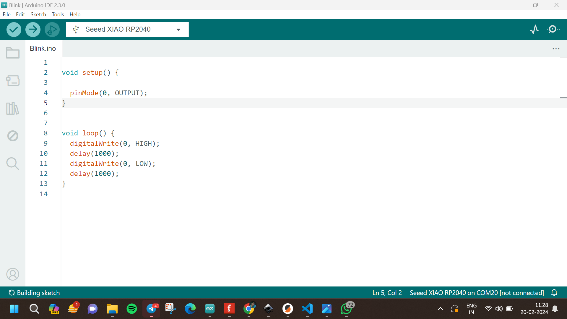
i stared with an initail power of the board using the uab C cable and made sure that it is powering up with out any issues
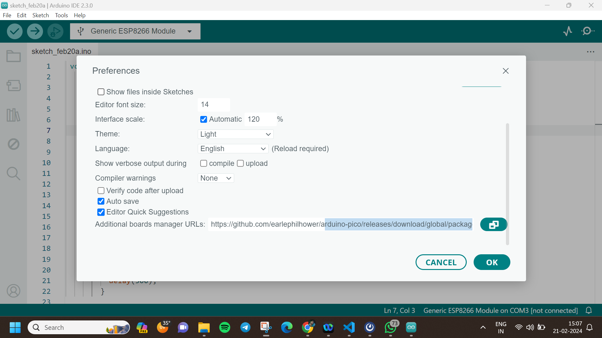
to start with i have also got expeince in proggarmneing the rp2040 boards i started up the arduino software and the added the board using the board maneger url and then from tools selected the board as seed studio xiao and the nessery com port and started with the first proggrame being the blink sketch. before that i used the usb c cable and powerd the board up to see that it is alive and well and it responded well so i procced to test the leds
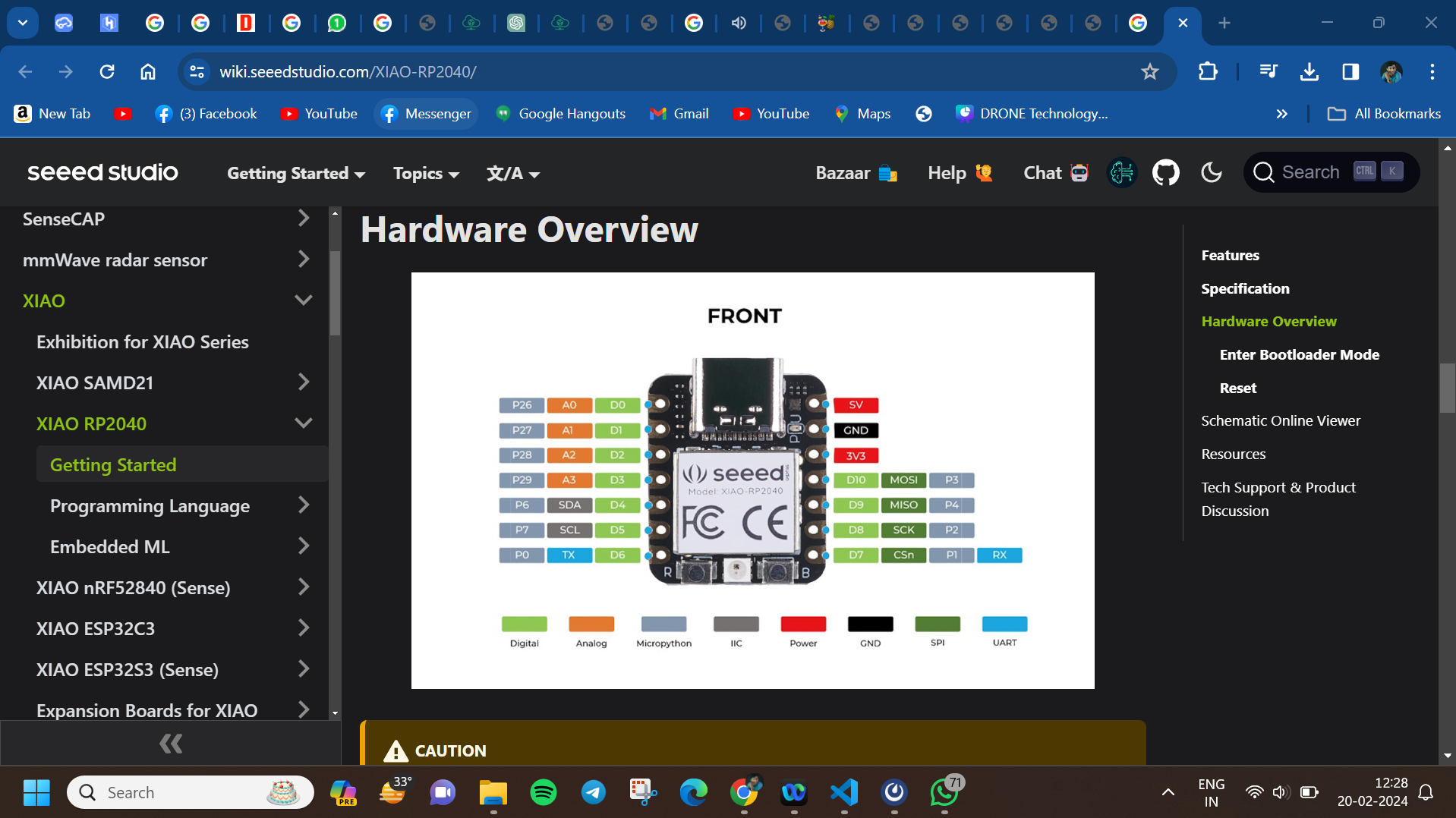
in order to understand the pinouts i went to the official wiki of seeed studio and looked up the pinout digram and configuerd it in the code
i used the arduino as my IDE for programing and debuggingg
so we stared with createing a stencil using papper and made a small rig by sticking together pcbs
after i put my pcb inside and put some lead paste on top and wiped it in to the stencil using a credit card and got a good layer of lead
then i placed the 3 components in and moved to the reflow oven and setup the reflow curve and put the pcb inside, then we took it out and used a microscope to look for shorts and corrected it using the soldering wick and isnpecting the pcb
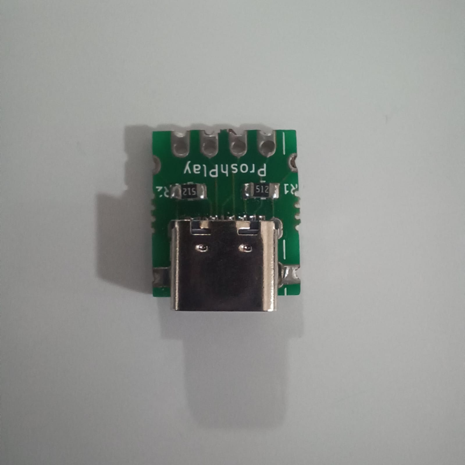
so this is the final assembled usb C brake outboard
A FAILED ATTEMPT
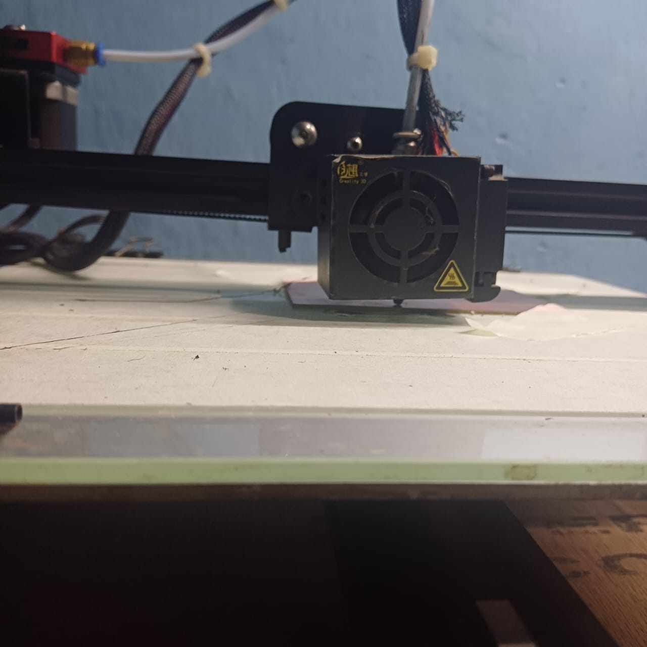
after finishing the assigments i moved on to do somthing diffrent while in the class something really strck me to make a trace using 3d printer so i used my home 3d printer the criality cr10 and attempted to put a layer of trace on top of a piece off copper clad
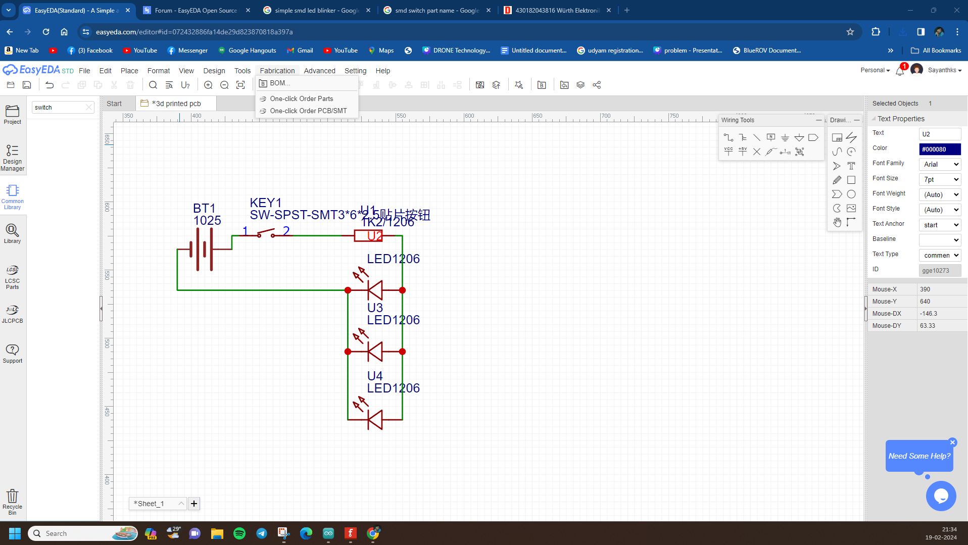
i fired up easy eda and made a small led circuit with a switch and few leds
then i exported the dxf file and opened it in fusion 360 and procceded to extrtued the trace and used the pursa slicer to slice the files for printing
then loded up the printer with PLA (a really bad choise that i later regreted on ) then set the z of set as the hight of the pcb and stared to print the first layer but it failed agein and agein to stick then i used a piece of emery to rough the surface it also dident work out then i blasted the bed to a temprature of 90 that aslo did'nt work then after 20 failed attempts and 3 coffes later i addmited the deffet
i later found out that pla is littrely impossible to stick on shiny surfaces you can get some good results by using TPU but i didnt had anything laying around so i submitted the surender, pllaing to revist this experiment soon
 group assingment
 link to Quentorres
s.jpeg)
s.jpeg)
.jpeg)