Electronics Design
Individual assignment:
Group Assignment:
The group assignment I learned how to use a multimeter and an oscilloscope. These tools demonstrated the ways that voltage moves through a circuit board, depending on where you attach the multimeter. For example we were able to measure that the resistor was harnessing 3.1v and the LED it led to was operating at 1.8v, these added together equal 4.9v, which was the amount of voltage given through the 5v pin. Even though 4.9 is not equal to 5, this proves that some voltage is lost in the process of moving through the circuit. The oscilloscope was very interesting to learn how to use because of it different capabilities/settings, and its ability to visualize the current of the circuit.
Setting Up KiCad and the Fab Components Library
I used KiCad to design my developement board. I followed the programs instructions for installation and kept the default settings.
After opening a new project in KiCad I downloaded Fab Academy's library of fab components using these
files and instructions. The components now appear in the libraries under "fab."
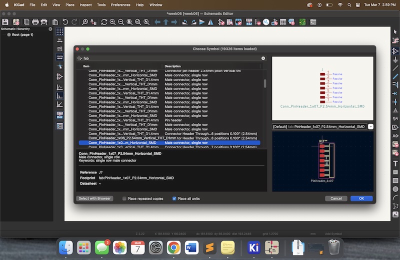
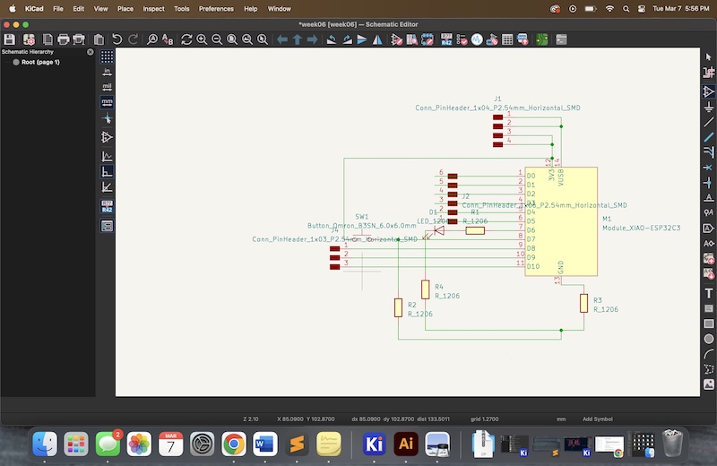
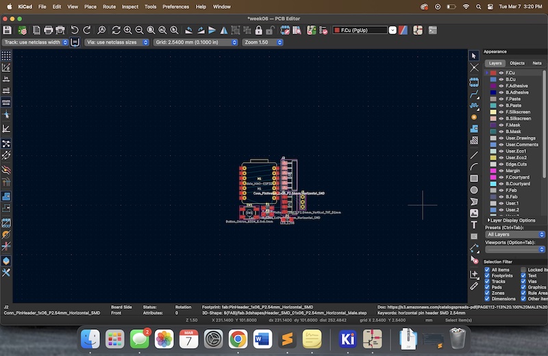
Using the Schematic Layout editor I placed the components of the developemnt board using the fab library and wire tool.
Following the teachings of my instructor, I used the XIAO-ESP32C3 chip to create my developement board with an LED, button, and a total of 13 pins.
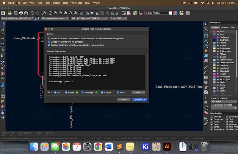
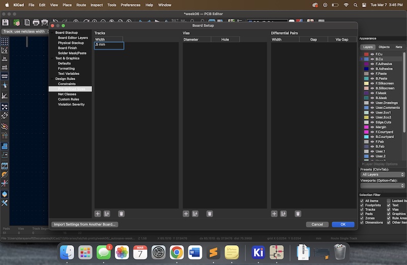
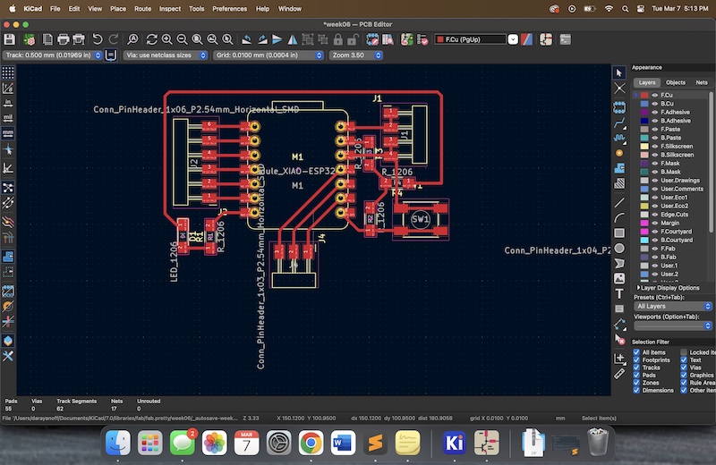
I then arranged the layout in the PCB editor. To do this I had to update the PCB editor to include the changes I made to the Schematic. I also had to change the width of the traces to .5mm to cater to the mill, which cannot create smaller.
 <
<
This was quite the challenge! I had to edit the components in the Schematic Editor a few times to get the right arrangement. To enable the creation of the board without intersecting wire traces, I had to add two resistors to my design that I intend on make 0ohms. In this way they will act like tiny bridges that can jump over other traces.
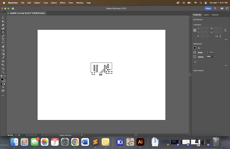
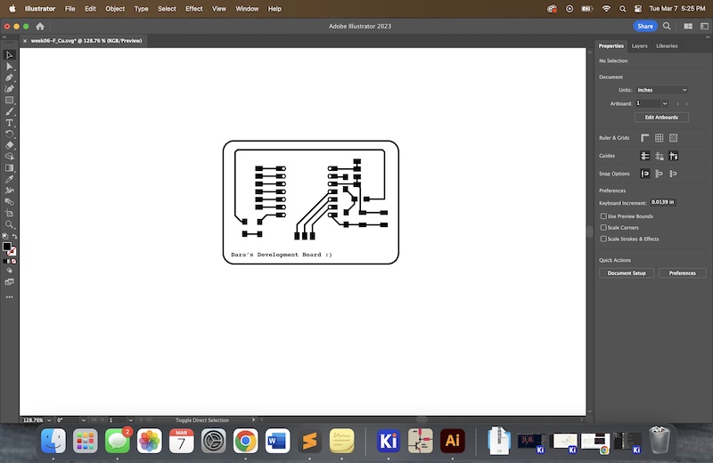
Using Adobe Illustrator, I added a border to my developemnt board by exporting the file from KiCad as an SVG. Using the rectangle tool, I created a rectangle that surrrounded the board and its components. Then using the test tool I added the label "Dara's Development Board :)."
Development board finished!