Operate the Mill for PCBs
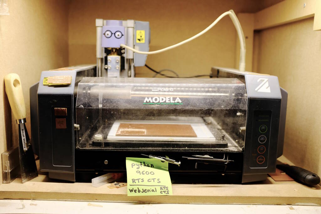
At Waag we are using the Roland Modela MDX-20 that we operate from Mods.
Let's first discuss some of the design rules for this machine
Design Rules
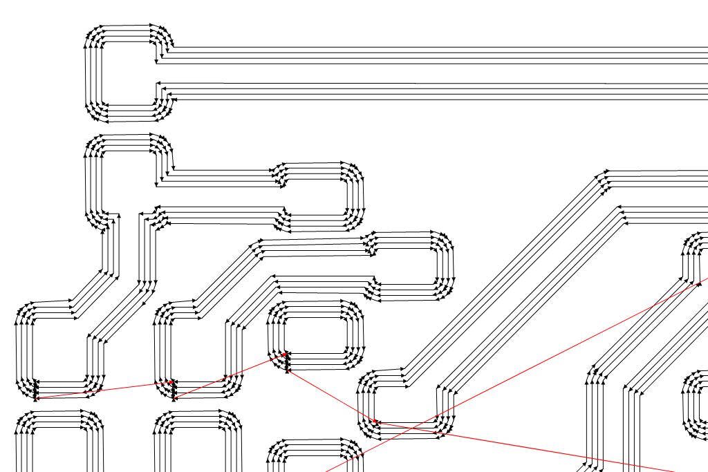
We provide Mods with a PNG with high resolution (1000 dpi or higher) or SVG. Most likely these files need to be inverted to make sure that the area around the traces is cut away instead of the traces.
We use a 2-flute end mill with a diameter of 0.4 mm for milling the traces and a 2-flute end mill with a diameter of 0.8 mm for the board edges. Mods has a good set of default parameters for our machine with a cut speed of 4 mm/s and a jog speed of 2 mm/s. The depth of the trace with 0.0025 in is clearly not enough:
So, a cut depth of 0.004 in is what we use and works well on the copper layer of the boards that we use. For the board cutouts, we use the cutting depth of 0.024 in and we set the max depth to the thickness of the plate to mill and some more. For example for a plate of 1.45 mm tick, we used 1.55 mm as max cutting depth.
A good offset number and stepover is what Mods has as default values which is 4 and 0.5 respectively. We use forward as path order and climb for cutting direction.
For tooling Henk made clear that all the tools that you need for the PCB mill stay inside the closure for the mill. This is true for the hex keys to insert mill bits, spatulas for removing the sacrificial or copper plate, and the screwdriver to wiggle out a just milled PCB.
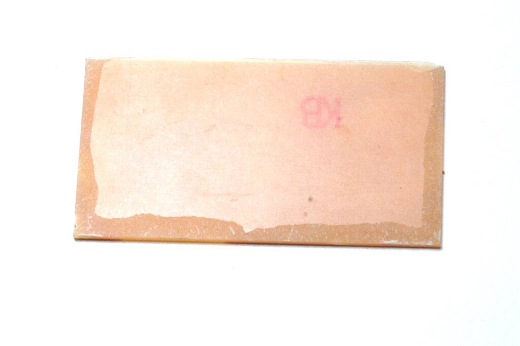
The plate for the boards has three layers: a transparent acrylic plate with a white plate on top melted to the glass plate with acetone. This white plate is flattened by means of milling making it perfectly perpendicular to the mill. On top of that plate goes a sacrificial copper plate fixated with double-side tape on which we attach the PCB board that we want to mill, also with double-sided tape. Changing the sacrificial copper plate can be done with the spatula after which we remove the tape rests with tape remover.
Checklist for Preparing SVGs from KiCad
Assuming you're happy with the PCB layout in KiCad, export the SVGs to mill with the following settings:
- Choose File ➜ Export ➜ SVG
- As Print Mode choose "Black and White"
- As SVG Page Size choose "Board area only"
- Uncheck "Print board edges on all pages"
Then do the actual export with:
- Select "F.Cu" for Copper Layers
- Choose "Export"
- Unselect "F.Cu" and select "Edge.Cuts" for Technical Layers
- Choose "Export"
Important in this list is to only use the board area and disable the board edges.
Checklist for Milling a PCB
For this list, we assume that we created an SVG as described above in KiCad.
- Change to the right mill bit, mind to use the screw that Henk marked!
- Make sure that the mill bit is inserted "high"
- Load the SVG with traces in Mods
- Invert it
- Choose for "set PCB defaults" "mill traces 1/64"
- Verify the tool diameter (0.3962 mm)
- Verify the cut depth (0.004 in)
- Verify the max depth (0.004 in)
- Verify the offset number to be 4
- Verify the stepover to be 0.5
- Verify the direction to be climb
- Press calculate
- Lower the Z on the machine, it should not hit the copper plate
- Possibly lower the bit a bit more for more precision in finding the right location.
- In Mods, go to the bottom right to "WebSerial", press "Get Device" and select "/dev/usbTTY0"
- Go to Roland MDX / iModela and set the origin to where you want to start milling (the bottom left).
- Record this x and y position (for if the page needs to be reloaded).
- Bring the Z all the way down on the machine
- Important: Raise the Z a bit (at least more than the max cutting depth)
- Lower the mill bit to touch the copper plate, mind to use the screw that Henk marked! Grab the mill bit with two fingers and hold it down actively to make sure it really touches the copper layer while fastening the screw that holds the mill bit.
- Press calculate again in Mods
- Send the file
After milling remove the dust from the plate. Then to mill the outline:
- Change to the 0.8 mm mill bit, mind to use the screw that Henk marked!
- Make sure that the mill bit is inserted in a high position again.
- Load the file with the edge cuts.
- Invert the file again.
- Measure the thickness of the plate.
- In Mods, choose "mill outline (1/32)".
- In "Mill raster 2D" set the max depth to the thickness you measured + some more, for example 1.55 mm if you measured 1.45 mm.
- Verify the tool diameter (0.7924 mm)
- Verify the cut depth (0.024 in)
- Verify the offset number to be 1
- Verify the stepover to be 1
- Verify the direction to be climb
- Move to the origin you used above.
- Move the Z all the way down.
- Move the Z up (more than the max depth that you used)
- Lower the drill bit onto the plate, mind to use the screw that Henk marked! Take care that the mill bit really touches the copper plate, see above.
- Press calculate
- Send the file
Preparing the Design of the Board
My board will simulate the final project. It has temperature sensor and an LED that simulates the heating element. When it is on, it is supposed to heat the water. The board has two buttons to increase and decrease the temperature of the water (the threshold to turn the heater on or off). A buzzer signals that the water is on the temperature and another LED simulates a strip of LEDs that signal the closed eyes that 5, 10, or 15 minutes have passed.
Selecting Footprints
When selecting footprints in KiCad in the Electronics Design week I made use of the Fab library, however, I learned that that doesn't necessarily mean that we have the components. Instead I should look at the Fab Acadmey Inventory to find the parts and their data sheets.
The datasheet of the LEDs state that the forward voltage is typically 2.0 V taking 20 mA of current. Since a pin on the RP2040 can only deliver 12 mA of current at 3.3 V, I should compute with these numbers. The resistor that I have to connect serially to the LED needs to experience a voltage drop of 3.3 - 2.0 = 1.3 V with a current of 12 mA, R is V/I = 1.3 / 0.012 = 108 Ohm. The closest resistor is 100 Ohm and the next one 330 Ohm. I wanted to go with 330 Ohm to be safe, but the box with 330 Ohm resistors was empty, so I went for 100 Ohm afterall.
The Fab Inventory does not have buzzers but they were in stock at Waag. However, there was no identifying information, so I searched for similar images and it's very likely that the one we have is the BSP1407M-20 . The component can take a voltage between 1 and 20 V but a max current of 3mA. This means that we need to serially connect a resistor of R = V/I = 3.3 V / 0.003 A = 1100 Ohm. The closest is a 1 kOhm resistor.
Since there is no footprint for this component, I chose a standard buzzer and moved a pad manually to a distance of 14 mm. When soldering I found out that I should have given the pads a bit more space. The pads now disappeared under the buzzer complicating the soldering.
It was not clear which temperature sensor I selected but it turned out that I selected the 1 kOhm RTD sensor from the Fab Inventory that we had in stock. Since it is connected to 10 kOhm resistor on 5V, the current the sensor experiences is I = V/R = 5 / 10000 = 0.0005 = 0.5 mA which is not in the specification of 0.1 - 0.25 mA, now that I'm writing this. This is strange and will investigate this further below. Anyhow, I created the board with this sensor and will come back to this issue later.
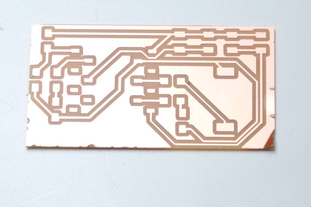
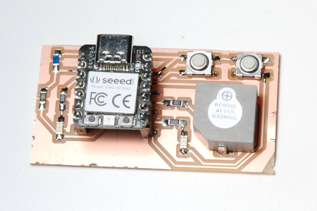
In any case, this is the schematic of the board I created:

After creating a footprint, I consulted Henk that said that I could make the board a lot smaller and rearrange the buttons to put them next to eachother. The final footprint assignment is as follows, note the pad that I moved for the buzzer:

I exported the footprint as above to mill it.
Milling the PCB
The milling process went well in general.
Setting up Mods
While setting up Mods I made the following mistakes: I forgot to invert the SVG and my experience from the group assignment was not enough to recognize that the view of the traces was wrong:
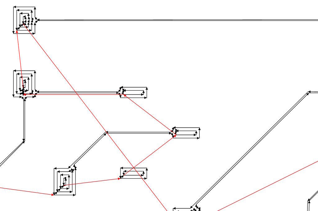
Henk pointed this out to me and when I inverted the SVG image, I immediately recognized how correct paths should look like:
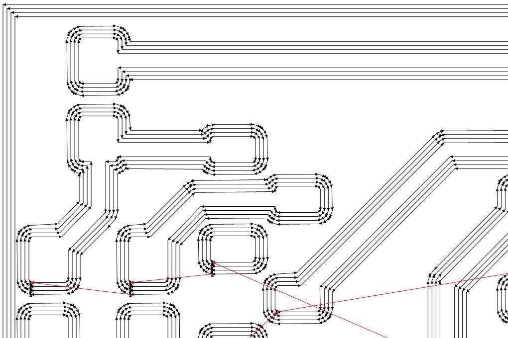
However, I also noticed a border and found out that KiCad has an option enabled by default that exports the bord edges. Disabling the board edges resulted in correct milling paths:
Milling the Traces and Edges
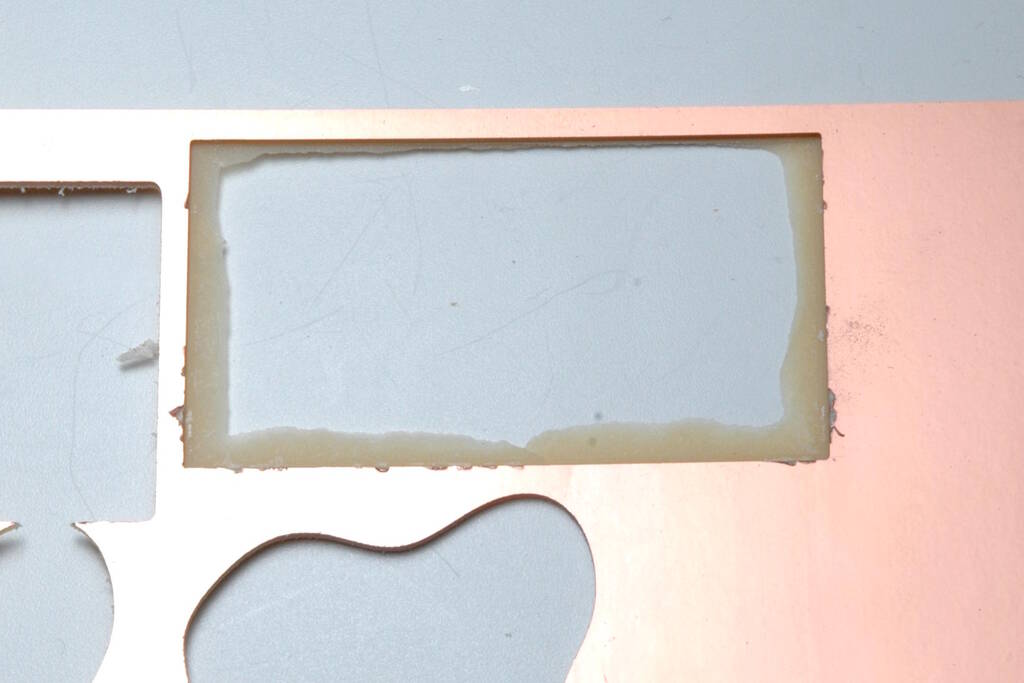
Milling the traces went perfectly. With milling the edges I made a couple of mistakes. I measured the board to be 1.55 mm thick and I used this as setting. But when I tried to remove the plate it didn't move and I damaged a bit of a copper edge. This was not a conductor, so no big problem. I decided to mill again with a maximum depth of 1.65 mm.
After completion, the board seemed stuck again, but when I applied some force I could see some movement, so I applied more force. The board came off, but it turned out that I simply broke the edges:
After measuring the board, it turned out to be 1.55 mm, so it is strange that the mill hadn't been able to go deeper. Most likely, when I raised the Z-axis, I raised it less than 1.65 mm, resulting in a situation where the mill bit couldn't get low enough.
The board itself looked good, but with some damage on the edges:
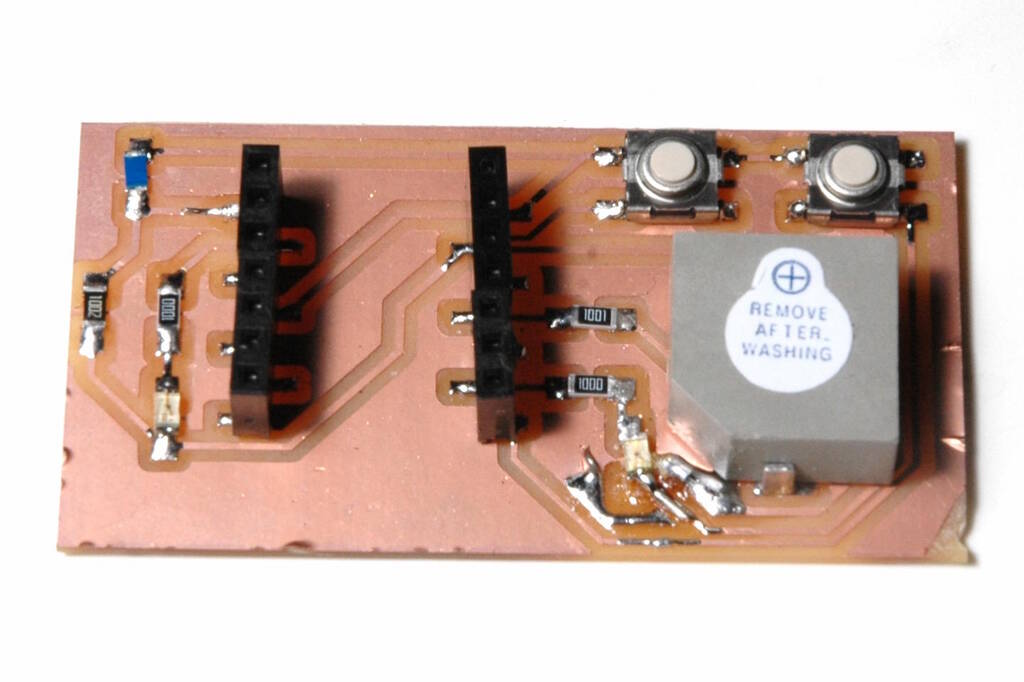
Soldering the Board
The soldering process went well. I started with the smallest components to make sure that the large components wouldn't be in the way when soldering smaller ones. I first applied some solder to one pad, placed the component with tweezers, and reheated the solder on the pad to fixate it. I would then solder the other pad: I keep the soldering tip to the side of the component and the pad, wait 5 seconds, apply some solder, remove the solder, and remove the soldering tip.
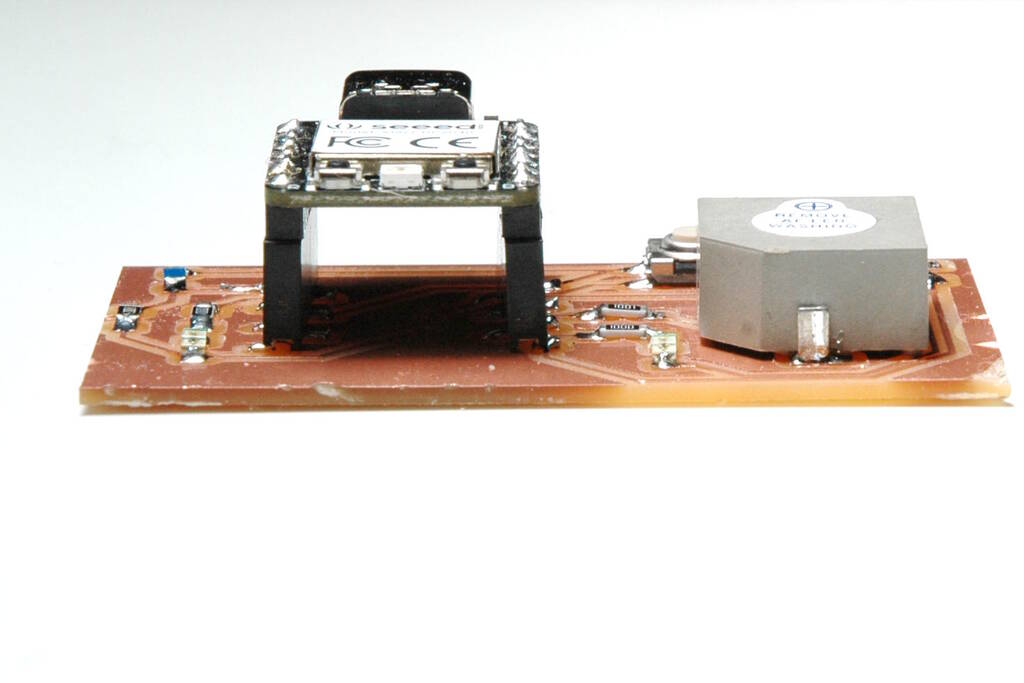
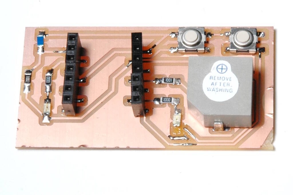
The soldered board:
From the side:
Programming the Board
I experienced quite some problems programming the board. Firstly, Arduino turned out to be a misfit with my design and it appeared that I made mistakes while soldering.
Arduino and Pull Down Resistors
Arduino started with the ATMega microcontrollers and these microcontrollers don't have internal pull down resistors. However, the RP2040 does have internal pull down resistors and I designed my board to make use of them.
What I didn't expect is that Arduino doesn't have an API for internal
pull
down resistors. You can state:
pinMode(PIN_BUTTON, INPUT_PULLUP);
,
but not
pinMode(PIN_BUTTON, INPUT_PULLDOWN)
or something similar.
I'm not fond of Arduino anyway, because I have to use Arduino IDE which is completely different from my Emacs workflow. So, I decided to switch to plain C.
The RP2040 SDK
On Arch Linux there is an
AUR
package
for the Pico SDK (
pico-sdk
), so I installed that and I cloned the
pico-examples
repository:
git clone https://github.com/raspberrypi/pico-examples.git
I then built everything in the following way:
      cd pico-examples
      export PICO_SDK=/usr/share/pico-sdk
      mkdir build
      cd build
      cmake .. -DPICO_BOARD=seeed_xiao_rp2040
      cd blink
      make
I could then press the boot button while connecting and then mount the
drive and copy
blink.uf2
to the drive. Blink worked perfectly.
I did the same with
hello_world_usb
and could read the output with:
picocom -b 115200 /dev/ttyACM0
So, we can conclude that we can work with the SDK for the RP2040.
Setting up the Programming Environment
I want to program in a comfortable way, which means that I want to work in
a separate directory, not in the
pico-examples
directory. This
means that I need to find a way to create a CMake file with which I can
compile my code stand-alone. So, I want to have a directory
simulate-device
with my C code and a CMake file such that it uses
the Pico SDK and compiles.
I also have to look up constantly what the GPIO number is for every pin on
the XIAO board, so, I want to define the pin numbers as well. Then it is a
hassle to constantly copy the
.uf2
file to the directory, so it
would be great if I could do
make push
to load the firmware.
To accomplish this, I created an
init.cmake
file that I place in
..
(can be used by other projects as well). The contents:
# Check for PICO SDK
if (DEFINED ENV{PICO_SDK_PATH} AND (NOT PICO_SDK_PATH))
    set(PICO_SDK_PATH $ENV{PICO_SDK_PATH})
    message("Using PICO_SDK_PATH from environment ('${PICO_SDK_PATH}')")
endif ()

set(PICO_SDK_PATH "${PICO_SDK_PATH}" CACHE PATH "Path to the Raspberry Pi Pico SDK")

get_filename_component(PICO_SDK_PATH "${PICO_SDK_PATH}" REALPATH BASE_DIR "${CMAKE_BINARY_DIR}")
if (NOT EXISTS ${PICO_SDK_PATH})
    message(FATAL_ERROR "Directory '${PICO_SDK_PATH}' not found")
endif ()

set(PICO_SDK_INIT_CMAKE_FILE ${PICO_SDK_PATH}/pico_sdk_init.cmake)
if (NOT EXISTS ${PICO_SDK_INIT_CMAKE_FILE})
    message(FATAL_ERROR "Directory '${PICO_SDK_PATH}' does not appear to contain the Raspberry Pi Pico SDK")
endif ()

set(PICO_SDK_PATH ${PICO_SDK_PATH} CACHE PATH "Path to the Raspberry Pi Pico SDK" FORCE)

include(${PICO_SDK_INIT_CMAKE_FILE})

set(PICO_BOARD "seeed_xiao_rp2040")

# include(pico_extras_import_optional.cmake)
Then I created a header file
xiao_rp2040.h
that contains the pin
numbers as advertized on the Seeed page:
#ifndef XIAO_RP2040_H
#define XIAO_RP2040_H

#define A0 26
#define A1 27
#define A2 28
#define A3 29

#define D0 26
#define D1 27
#define D2 28
#define D3 29
#define D4 6
#define D5 7
#define D6 0
#define D7 1
#define D8 2
#define D9 4
#define D10 3

#define BUILTIN_LED_R 17
#define BUILTIN_LED_G 16
#define BUILTIN_LED_B 25

#define PIN_SERIAL_TX 0
#define PIN_SERIAL_RX 1

#endif
Then finally, I use the following CMake file
CMakeLists.txt
to
compile the program:
cmake_minimum_required(VERSION 3.12)

include(../init.cmake)

project(simulate-device C CXX ASM)

set(CMAKE_C_STANDARD 11)
set(CMAKE_CXX_STANDARD 17)

if (PICO_SDK_VERSION_STRING VERSION_LESS "1.3.0")
    message(FATAL_ERROR "Raspberry Pi Pico SDK version 1.3.0 (or later) required. Your version is ${PICO_SDK_VERSION_STRING}")
endif()

# Initialize the SDK
pico_sdk_init()

add_compile_options(-Wall
        -Wno-format          # int != int32_t as far as the compiler is concerned because gcc has int32_t as long int
        -Wno-unused-function # we have some for the docs that aren't called
        -Wno-maybe-uninitialized
      )

add_executable(simulate-device
  simulate-device.c
  xiao_rp2040.h
)

add_custom_target(push)
add_custom_command(TARGET push
  COMMAND mnt usb sda1
  COMMAND cp simulate-device.uf2 /home/pieter/mount/usb
  COMMAND mnt unmount usb
  COMMAND sleep 2
  COMMAND picocom -b 11520 /dev/ttyACM0
  )

pico_enable_stdio_usb(simulate-device 1)

# pull in common dependencies
target_link_libraries(simulate-device pico_stdlib hardware_adc)

# create map/bin/hex file etc.
pico_add_extra_outputs(simulate-device)
Note the custom target
push
and the command below: It mounts
sda1
(which is typically the drive of the Xiao board when I enable
boot mode), it copies the
.uf2
file to the drive, unmounts it and
sleeps for 2 seconds. Then it automatically opens the serial terminal to
see the output.
The usage is as follows below, assuming we are in directory
simulate-device
. We first have to create and populate the build
directory:
      mkdir build
      cd build
      cmake ..
From this point on we can change the source code and in the
build
directory, we can then do the following to compile:
make
And to run it, we can do the following:
make push
Programming the Board
Programming the board showed several problems. First I tried the LEDs, then the buzzer, then the buttons, and then the temperature sensor.
The LEDs
It turned out that the LEDs were reversed. I had recently read an article about solid state batteries where I learned that a cathode was the positive pole. I remembered this, looked up in the data sheet where the cathode was and soldered them on the board with the cathode towards the pin.
This turned out to be wrong because cathode/anode says something about the flow of charge and in the case of a diode, the cathode should be connected to ground.
The buzzer
The buzzer worked but in a different way than I expected: It turns out that the buzzer is a small speaker and it gives a little "tick" when switching from positive to negative. In essence, I should send a wave form to it. I haven't done that because the little "tick" that I hear, already shows that it works.
The buttons
The buttons have given me quite a headache. The left/decrease button is the decrease button that is connected to digital pin D3. Note that this pin can act as an analog pin as well. The right/increase button is connected to digital pin D7. The design is such that they should be pulled down, so I used the following code to initialize both pins:
  gpio_init(PIN_BUTTON_DEC);
  gpio_set_dir(PIN_BUTTON_DEC, GPIO_IN);
  gpio_pull_down(PIN_BUTTON_DEC);
  gpio_set_input_enabled(PIN_BUTTON_DEC, 1);

  gpio_init(PIN_BUTTON_INC);
  gpio_set_dir(PIN_BUTTON_INC, GPIO_IN);
  gpio_pull_down(PIN_BUTTON_INC);
  gpio_set_input_enabled(PIN_BUTTON_INC, 1);
Interestingly, the increase button works as expected, but the decrease button is always high. I will discuss this problem in the section below.
The temperature sensor
I test the sensor in the following way but it always yields the maximum value:
adc_init();

adc_gpio_init(PIN_THERMISTOR);

adc_select_input(0);

while (1) {
  const float conversion_factor = 5.0f / (1 << 12);
  uint16_t result = adc_read();
  printf("Raw value: 0x%03x, voltage: %f V\n", result, result * conversion_factor);
  sleep_ms(500);
}
Since this uses an analog pin and the problem with the button is also on an analog pin, these issues may be related. After investigating example circuits for RTD sensors, it becomes clear that I designed the circuit for an NTC sensor and I now understand that they can not be interchanged. I assumed that thermistors always worked in the same way and the circuit I created was "the" way to measure thermistors.
Since it is clear that the circuit is wrong for this sensor, I didn't investigate further.
Debugging the Issues
In this section we discuss the debugging of the LEDs and of the buttons.
Changing polarity of the LEDs
I needed to desolder the LEDs, flip them, and solder them back. Although the first one went well, for the second one, I accidently ripped the pad from the board...
I tried to get the pad off of the LED but this didn't work. There was a small gap and I tried to bridge between the LED and the small trace that was left. I didn't know how to do it and Henk told me to just "pruts" which means basically "messing around". Well, I did that but didn't succeed. I used so much solder that there was a layer of flux on top of the wire.
In the end, Henk came end showed me how it's done. He first removed excess solder with a vacuum pomp:
Then he tried to bridge it which was interesting to see. He essentially tried to guide the solder from the trace to the LED. This didn't work in the end and then he used a small wire to connect the little trace to the LED.
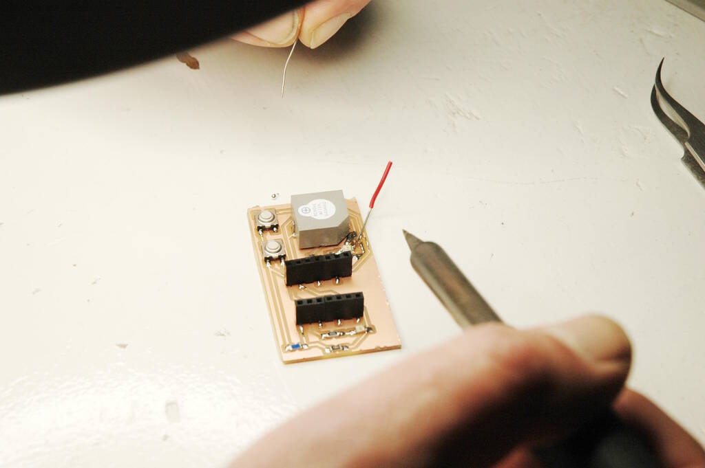
He had to use flux from a needle dispenser to solder the trace.
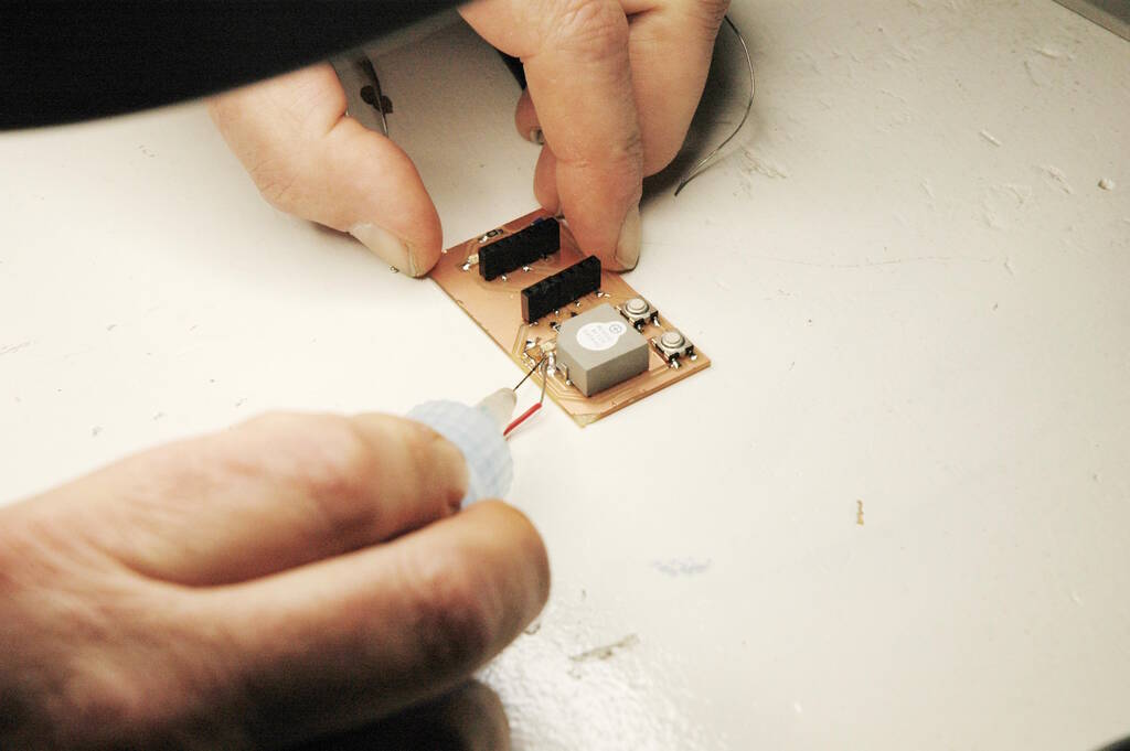
In the end we had our Frankenstein board...
The Buttons
The decrease button doesn't work as expected, so let's describe the problem first (following Henk's lecture on debugging).
Expected Behavior
Both buttons are "off" by default and when pressing one or both buttons they switch to "on".
Observed Behavior
The decrease button is always on while the increase button is "off". When pressing the increase button, it simply switches to "on" as expected. When pressing the decrease button, the value remains "on" but we can see the LEDs light up a bit. This could potentially be explained by the fact that the buttons are switched with 5V instead of 3.3V. When measuring the pin of the button, we measure a voltage of 3.56 V.
Additionally, when we remove the RP2040 from its socket, the decrease button switches to "off".
Hyphothesis: a short circuit on the board
Since the button switches to "off" when the RP2040 is removed from the socket, we can conclude that it is not the microcontroller that somehow drives the pin with a voltage. This must mean that the pin is driven from somewhere else. Most likely there is a connection between the trace and some other pin that has 3.56 V.
Using the connection measurement on the multimeter, I tested a connection between the trace and each other pin/trace. I couldn't measure any connection between any of the pins.
Hypothesis: the button is malfunctioning or soldered incorrectly
It could be the case that I soldered the button incorrectly, 90 degrees turned for example. However, when measuring with the multimeter, the connection is made between the right pins when pressing the button.
Hypothesis: the pin is in the wrong mode
Since digital pin D3 can also be configured to be analog pin A3, it may be the case that the pin is configured incorrectly. First, I checked whether I can actually use it as a digital input pin, but the datasheet confirms that this is the case.
I consulted the SDK documentation to find functions to check for functionality to check the pins. For both pins I print which function it is in and whether it is pulled down:
printf("func inc: %d\n", gpio_get_function(PIN_BUTTON_INC));
printf("pulled down? %d\n", gpio_is_pulled_down(PIN_BUTTON_INC));
if (gpio_get(PIN_BUTTON_INC)) {
  puts("inc on");
}
 else {
   puts("inc off");
}

printf("func dec: %d\n", gpio_get_function(PIN_BUTTON_DEC));
printf("pulled down? %d\n", gpio_is_pulled_down(PIN_BUTTON_DEC));
if (gpio_get(PIN_BUTTON_DEC)) {
  puts("dec on");
}
else {
  puts("dec off");
}
puts(" ");

sleep_ms(200);
It turns out that the pins are in the same and correct modes "SIO" (which is a mode for the "Single-cycle IO Block"). Both were also pulled down. As we could see above, I also explicitly enabled the input.
Next steps
At this time, I'm at loss to explain the behavior. I'm now going to isolate the problems. For example, I will test a button on pin D3 to verify the behavior. I also have to create a new board and instead use an NTC thermistor because this is much easier to use.
Hypothesis: the increment button works in isolation
I use a small breadboard to check the D7 pin (the non-analog) pin. I first connected it to 3.3 V and there it works as expected. It also works on 5V.
Hypothesis: the decrement button works in isolation
When doing the same on the small breadboard but then connect it to D3, I expect the same behavior. Indeed, the button switches to "on" or "off" as expected, but the behavior is a bit different between 3.3 V and 5 V.
With 3.3 V, the button works exactly the same as on the D7 pin, but with 5 V, the behavior is different: The power LED of the board becomes brighter when the button is pressed. I think an analog port is perhaps not very good in taking a high voltage. In any case, because I see this behavior, I think I'm not going to switch with 5V anymore.
Intermediate Conclusions
Now that the pins work in isolation, we can reject the hypothesis that the pin D3 is in the incorrect mode. We can also conclude that connecting to 5V is not a good idea.
Hypothesis: putting 5V to A0 affects the pin D3
To verify whether 5V (with a low current) on port A0 affects reading a value from D3, I started measuring on the A0 pin. While testing the previous circuit while measuring, I noticed that the voltage measured on A0 changed on switching the button connected to 5V on port D3 (A3). Below a video where you can see the following: Pin D7 on the right is the pin that works as expected on 3.3 V and on 5 V. Pin D3 on the left is the pin that doesn't work as expected: Connected to 3.3 V it works as expected, connected to 5 V, we suddenly read 5V on a different pin A0:
After showing this to Neil, he immediately mentioned that all bets are off if you connect a pin to 5 V. I was confused because there is a pin for 5 V, but I now understand that these pins are not necessarily connected to the microcontroller. So, the board provides 5 V and 3.3 V via USB and these pins are board pins. The D1 and A0 pins are microcontroller pins and the microcontroller only accepts 3.3 V.
So, the fact that the D7 pin works as expected with an input of 5V is coincedence and it may or may not be the case that these pins are "5V tolerant" as Neil and Henk called it.
I wanted to check whether I could relate this information back to the data sheet and indeed I could: "Both the output signal level and acceptable input signal level at the pad are determined by the digital IO supply (IOVDD). IOVDD can be any nominal voltage between 1.8V and 3.3V".
Conclusion
The 5 V and 3.3 V pins are "board pins" and don't necessarily mean that they can be connected to the "microcontroller pins". So, using 5 V as input simply doesn't work.
Reflections
I learned so much this week that I don't know where to start. A summary: I understand the difference between board and pin types, the input and output voltage a microcontroller can handle, internal resistors for pull down / pull up, and on pins, different types of thermistors.
Pin Types on a Board
I have to make a distinction between board pins and microcontroller pins . A board is designed with a microcontroller and the microcontrollers has pins that may or may not be routed to the pins of the development board. The 5 V, 3.3 V, and ground pins on the board come from the USB connection and power the microcontroller (not the 5V one). The other pins may come from the microcontroller.
Voltages on a Board
I have to carefully check the output and input voltage and current in the datasheet of the microcontroller and for the RP2040 that is 3.3 V. The 5V pin comes directly from USB and is not wired to the microcontroller at all. So, the fact that there is a pin on the board that delivers 5V, does not mean that the microcontroller supports or is tolerant to it.
Current for Pins
Now that I understand that the 3.3 V pin on the board comes from the USB connection, it may provide a current that a pin cannot take. This, together with the fact that ATMega microcontrollers don't have internal pull down resistors made me think about my circuit for buttons: I now realize that my button circuit may be wrong, because I connect the button to 3.3 V and pull the input pin down with the internal pull down resistor. I assumed that when I press the button, that the internal pull down resistor also limits the current for a high signal, but looking in the datasheet I cannot find a resistor that limits the current.
Looking at several example circuits about pull down resistors, it appears that the following circuit that I used is a common one. It shows a button connected to VCC (should be 3.3 V on the RP2040) and when connecting, the pin notices a high signal. When the button is "off", the pin will measure a low signal because of the pull down resitor to ground.

My question is whether pressing the button does not overload the pin, suppose that the power source can deliver 1 A of current, for example. Is pressing the button then an issue or is there an internal resistance that prevents the current to become to high. Henk thinks there is indeed an internal resistance.
I will ask Erwin about this and I deciced to simply measure the current, so I measure the current by making the voltmeter part of the circuit between the pin and the button. Below is a picture of the measurement: you can see that the current is only 0.056 mA, which converts to an internal resistance of V / I = 3.3 V / 0.056 = 59 kOhm.
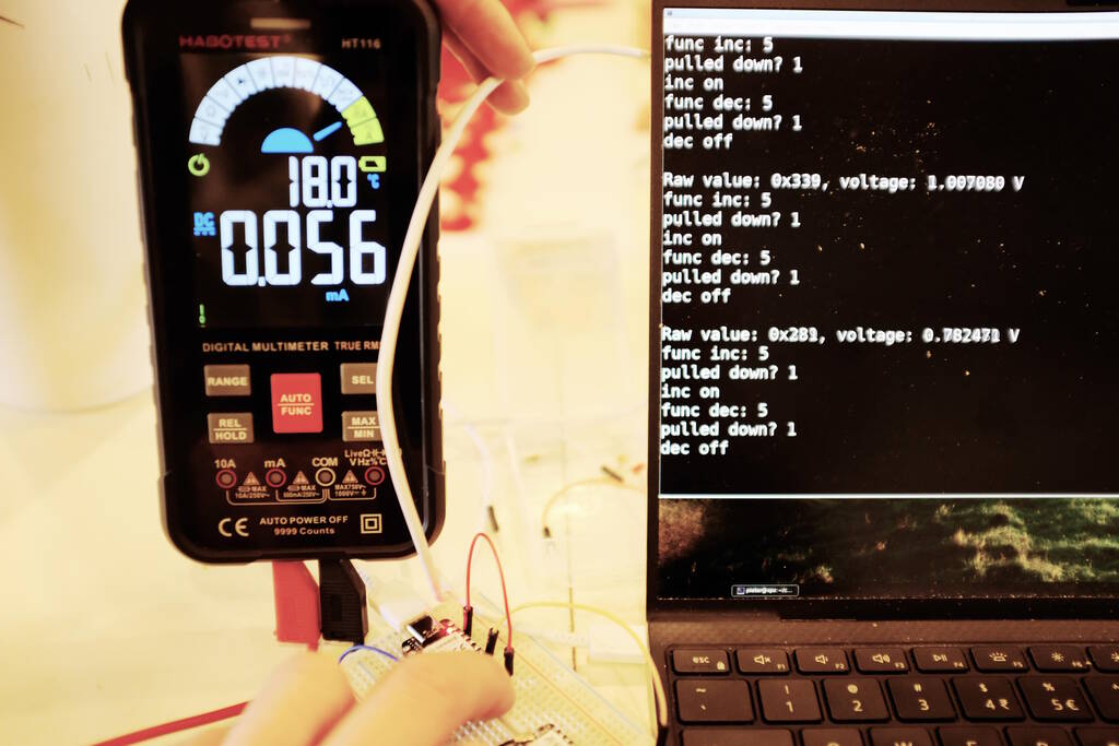
Erwin came back to me and indeed confirmed that pins only have to measure the voltage, so they typically have a large resistance of about 50 kOhm. Additionally, a power source may be able to deliver more current but this doesn't mean it will deliver it. This depends on the resistance.
So, we can conclude that there is an internal resistor and that this circuit is safe.
Anodes and Cathodes
I learned that anodes and cathodes have different meanings depending on the device. In devices that consume power, the cathode is associated with the negative side. In devices that deliver power, such as a battery, the cathode is associated with the positive side. However, if the battery is charged, the cathode would be the negative side. A good mnemonic is ACID: Anode Current Into Device.
So for a diode, the anode should be connected to the positive side, the cathode to the negative side. For a discharging battery, the cathode is the positive side because the current will go to the negative pole which is the anode. While charging, the positive side receives current, so that is the anode.
Thermistor Types
I wanted to use a temperature sensor and I learned about the class of temperature sensors called thermistors, that change resistance based on temperature. When selecting a footprint, I simply chose a thermistor and I ended up using an RTD thermistor. At least, I thought an RTD was a thermistor as well, but it turns out that that is not the case. An RTD is completely different sensor but uses resistance as well, but it requires a different circuit. So, what went wrong here: I assumed that one measures temperature with resistors that change resistance based on temperature and that an RTD is a thermistor as well. It is simply lack of knowledge and a frame of reference that led to these assumptions and mistakes.
Tasks
Fab Academy
- Characterize the design rules for your in-house PCB production process.
- Make and test the development board that you designed to interact and communicate with an embedded microcontroller.
- Described the process of tool-path generation, milling, stuffing, de-bugging and programming.
- Demonstrate correct workflows and identify areas for improvement if required.
- Documented that your board is functional.