The Future of Making and the OTFN Hackathon
Right after last Thursday's group assignment, I traveled to Hamburg to attend The Future of Making Conference , an event that marks the end of the INTERFACER Project of which I have had the honor to be part of, leading the work package called "The Open Source Hardware Ecosystem". My team and I from the Open Toolchain Foundation (OTFN) also organized a Hackathon around the Wakoma Nimble Wireless Mesh Router .
Both events were a great success. The conference was great to meet all the great people that formed the INTERFACER team, something that happened only once before at the Kickoff one year and a half ago when the project started. Given the short timespan I believe we achieved much with highlights such as Fab City OS Core and (shameless plug of the things of my work package) the Open Toolchain Foundation, Automated Documentation for Open Source Hardware, and OSH Tool, a tool for standardization for Open Source Hardware projects. Neil gave the closing keynote on the conference in which he shared his perspective on the developments around the goals of the INTERFACER Project, which was very interesting. I'm grateful that he took the time to acknowledge Daniele's and my work.
After this two-day event, we had a Sunday with some rest, but not really because we were preparing for the Open Toolchain Foundation's first ever Hackathon around the Nimble Wireless Mesh Router . I really think this must have been the coolest event I've ever attended even though I've attended conferences in India, Alaska, California, Phoenix and was part of a community build of an Open Source House in Belize organized by Open Source Ecology USA . (I know I must be biased because my team and I organized it, but it doesn't feel as if I'm biased.)
Introduction to Electronics
Last Wednesday, Erwin gave a very interesting lecture in which I finally could ask all kinds of questions about the gaps in my knowledge about electronics. I will list the filled gaps here.
While a resistor is a current-limiter without polarity on direct current , a capacitor is a current-limiter on alternating current . Capacitors can be in polarized (the electrolytic ones that are typically bigger) and in non-polarized form.
Capacitors are typically used to control debouncing : For example, when turning on a switch, there may be a brief moment in time where the switch is on and off many times. However, microcontrollers may be fast enough to pick this up, so by using a capacitor in the circuit you can alleviate this debouncing behavior.
Diodes have polarity and can be used to convert alternating current to direct current with rectifiers . LEDs can be light sensors if you connect them the wrong way. Diodes always have a forward voltage and current defined in the data sheet.
If capacitors act as resistors in alternating current , what acts as capacitors then? It turns out that coils act as capacitors in alternating current.
The terminology around transistors is a bit confusing. From my perspective there are four important types of transistors , there is the n-channel transistor, the p-channel transistor, the n-channel MOSFET, and the p-channel MOSFET. After some investigation, it turns out that what we commonly call a "transistor" is most likely a "Bipolar Junction Transistor", a BJT. This Stack Exchange answer explains it well, I think.
The difference between a BJT and a MOSFET is that the BJT is a device that is controlled by the current (the current in the base, determines the current that flows into the collector). On the other hand, the MOSFET is a device that is controlled by the voltage (the voltage across the gate determines how much current flows into the drain).
The n-channel and p-channel difference determines in what direction the current flows. An n-channel transistor has an n-type piece of silicon sandwiched between two p-type silicon plates and is also called PNP, whereas the p-channel transistor is sandwiched between two n-type silicon pieces, so NPN. The impurities and the amount thereof in these pieces of silicon determine how much it conducts and what the amplification factor is.
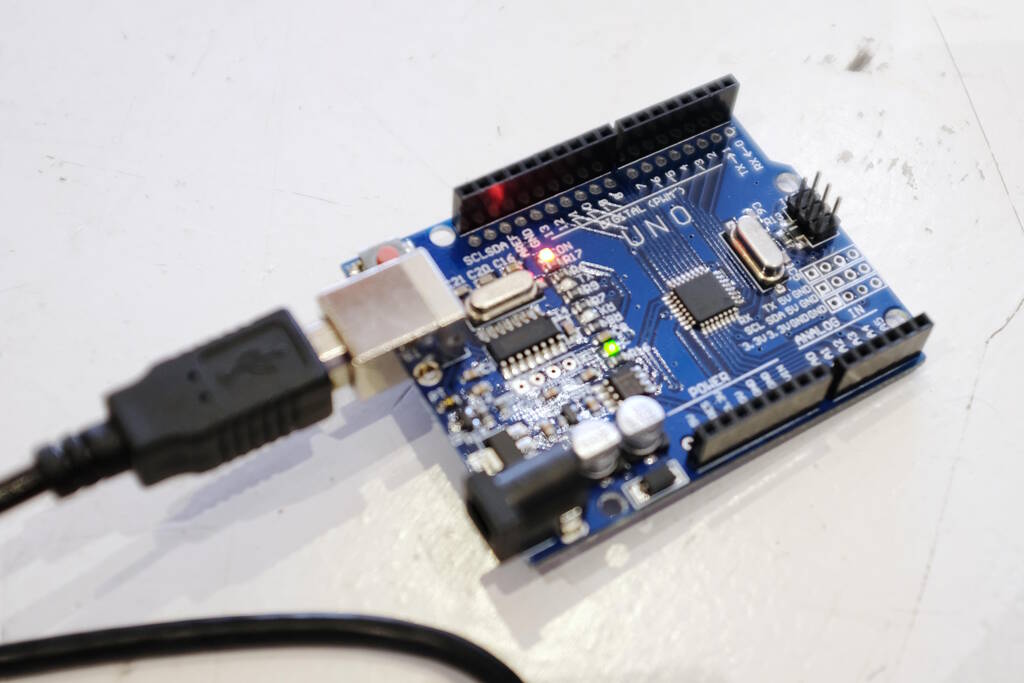
Observe the Operation of a Microcontroller
Erwin prepared an Arduino for us that we could observe in various ways. First, we decided to simply measure the pins with a voltage meter. This was a fun exercise that was kind-of a puzzle that we had to solve. The Arduino:
The Voltage Meter
We measured all the pins with a voltage meter although Erwin gave us the hint that we were only looking for digital signals.
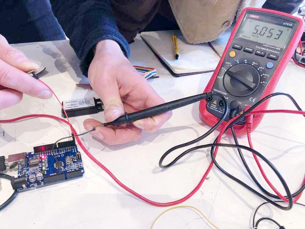
These are the values we measured:
| Port | Voltage (V) | Note |
|---|---|---|
| D0 | 5.0 | |
| D1 | 4.82 | |
| D2 | 1.1 | varying values |
| D3 | 0.8 | |
| A0 | -0.01 | |
| A1-A5 | 0.2 or 0.3 | |
| D4 | 1.4 | varying values |
| D5-D12 | 0.3 | |
| D13 | 1.1 | varying values |
| DREF | 0 | analog reference voltage |
| SDA | 0 | |
| SCL | 0.3 |
Now that we have this information, we want to take a closer look with the oscilloscope.
The Oscilloscope
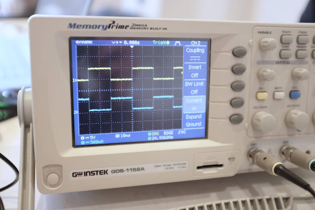
Using the oscilloscope was very interesting. We first measured pin D13 and we saw an alternating signal that lasted 20 ms. This means that we had a frequency of 50 Hz and Erwin confirmed that it was indeed 50 Hz. However, I wanted to hear the signal as well, so Michelle got us a buzzer and when we listened, I noticed that the tone was lower than what I expected from 50 Hz. We then looked more carefully and noticed that we had only looked at the length of the high or low signal but for a full wavelength, we need to look at the length of both the low and the high signal. This means that the signal does not last 20 ms, but 40 ms, giving us a frequency of 25 Hz.
Erwin expected 50 Hz as well, but when he checked the code he confirmed that he essentially made the same mistake, counting only the high signal. So, all in all on pin D13 we had a digital signal of 25 Hz:
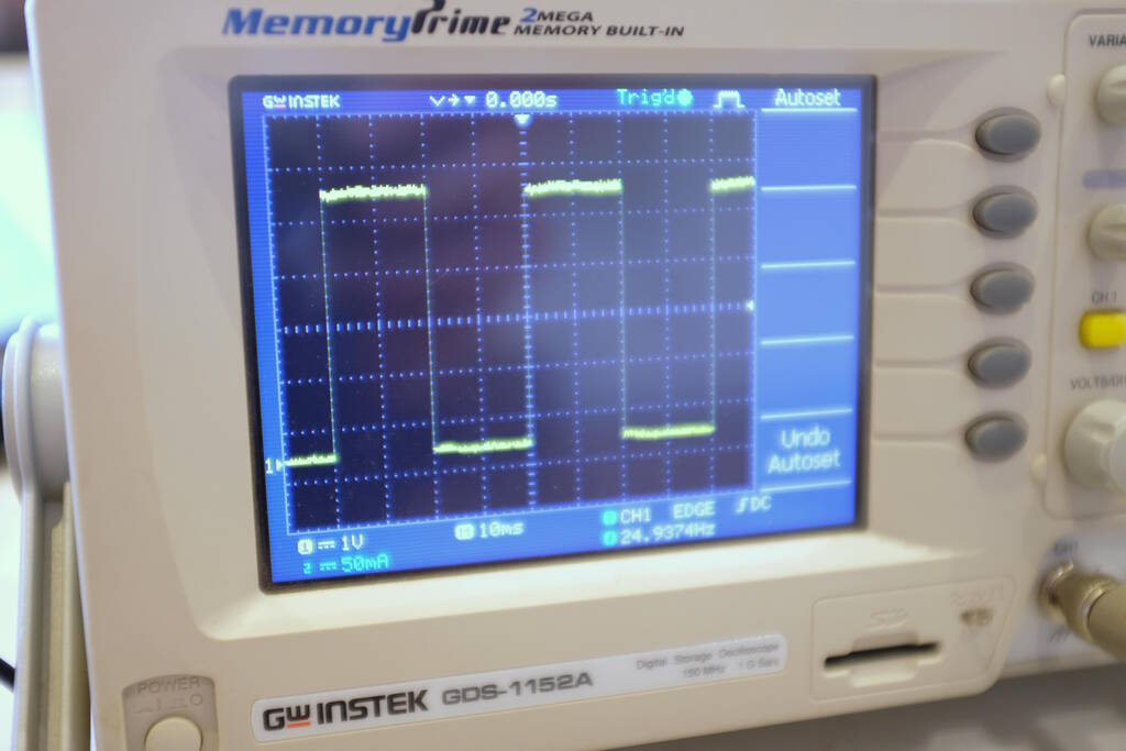
We then moved to D2 that had a frequency of 12.5 Hz as well:
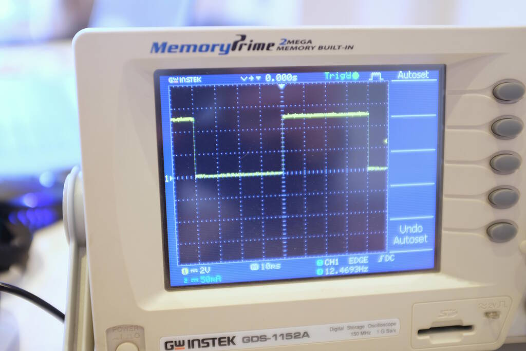
Pin D13 had a frequency of 16.6 Hz. Since we had two pins with a signal of 25 Hz, I was wondering whether the phase of the signal was the same or different. So, we measured both pin D2 and D13 and it turned out that indeed the phase was different:
Pins D0 and D1 had a high signal and D5 to D12 had a low signal. The table:
| Port | Digital Signal | Note |
|---|---|---|
| D0 | high | |
| D1 | high | |
| D2 | 25 Hz | different phase than D13 |
| D3 | 16.6 Hz | |
| D4 | 12.5 Hz | |
| D5-D12 | low | |
| D13 | 25 Hz | different phase than D2 |
Erwin's Code
The code that Erwin wrote to produce these digital signals is the following:
uint8_t i = 0;

void setup() {
  pinMode(2, OUTPUT);
  pinMode(3, OUTPUT);
  pinMode(4, OUTPUT);
  pinMode(LED_BUILTIN, OUTPUT);
  digitalWrite(2, 0);
  digitalWrite(3, 0);
  digitalWrite(4, 0);
  digitalWrite(LED_BUILTIN, 1);
}

void loop() {
  for (i = 0; i < 12; i++) {
    if (i % 2 == 0 ) {
      digitalWrite(2, !digitalRead(2));
      digitalWrite(LED_BUILTIN, !digitalRead(LED_BUILTIN));
    }
    if (i % 3 == 0) {
      digitalWrite(3, !digitalRead(3));
    }
    if (i % 4 == 0) {
      digitalWrite(4, !digitalRead(4));
    }
    delay(10);
  }
}
A note is that pin D13 is the pin for the builtin LED. So, the LED was pulsating with a frequency of 25 Hz. The conclusion is that we succesfully reverse engineered this little puzzle!
Discussion Final Project
I explained Erwin my ideas for a final project and he gave me some insights. Heating a considerable amount of water can most likely best be done with a wall socket, the 230 V we have. A triac is a transistor for alternating current and a solid-state relay essentially has a triac. For the pump, I could look into a peristaltic pump or using a simple DC motor that runs on 5V that I can switch on with a MOSFET.
For power, I could think of 230 V alternating current that powers the heating element that is switched on by the microcontroller with the solid-state relay. For powering the microcontroller and the motor, I could use USB powered by the 230 V giving 5V output.
Of course, I could look into reducing the amount of water and powering everything with 5 V. Erwin gave me the tip to look into how much energy it takes to heat water. From the top of his hat, he tought the value was 4.2 J per degree Celcius.
Finally, I mentioned that I've always wanted to study Maxwell's equations more thoroughly but that I'm held back because I feel I'm not familiar enough with differential equations. Erwin gave me the tip to look into the YouTube video Maxwell's Equations Explained from the channel Kathy Loves Physics and History .
Designing a Development Board
I will use KiCad to design my PCB. Fab Academy has its own symbols and footprints for various EDA software packages on GitLab, including for KiCad .
Initialization
Throughout this week, my system ( Arch Linux ) switched from version 6 to version 7 in the package repositories. Luckily I hadn't really started yet because of the conference and Hackathon. I'm now in the 5 hour train back, but my internet is not good enough to do an update. I think I can simply start in version 6 and migrate to 7 tomorrow or so.
After starting KiCad with the default settings, I created an empty KiCad project. I initialized the global symbol table by choosing Preferences ➜ Manage Symbol Libraries and choosing the recommended option "Copy default global symbol library table". I did the same for Manage Footprint Libraries.
I then created an empty project file for the board I want to design and
with this project open, I opened the same preference panels to install the
KiCad library (Preferences
➜
Manage Symbol Libraries
➜
Project Specific
Libraries
➜
Add existing library to table, and choose
fab.kicad_sym
).
Unfortunately, I got the following error message:
   Symbol library 'fab' failed to load.


   KiCad was unable to open this file because it was created with a more recent
   version than the one you are running.


   To open it you will need to upgrade KiCad to a version dated 20220914 or later.
That is weird, because I would assume that my version would be newer than that since Arch Linux is a rolling release. Let's check and I have version 6.0.11 which was built in January this year, so something is wrong with this error message or with my version. The release notes of KiCad also mention that my version was released on 26 January this year.
The Fab Academy KiCad repository had already an
issue
for this
by user
sgrc
who also pointed me to a
forum
post with a hack
that turned out to work:
diff --git a/fab.kicad_sym b/fab.kicad_sym
index 209c63e..b6f583f 100644
--- a/fab.kicad_sym
+++ b/fab.kicad_sym
@@ -1,4 +1,4 @@
-(kicad_symbol_lib (version 20220914) (generator kicad_symbol_editor)
+(kicad_symbol_lib (version 20210914) (generator kicad_symbol_editor)
   (symbol "Amplifier_Mono_LM4871M" (in_bom yes) (on_board yes)
     (property "Reference" "U" (at -7.62 10.16 0)
       (effects (font (size 1.27 1.27)) (justify left bottom))
Doing the same for the footprint library (Preferences
➜
Manage Footprint
Libraries
➜
Project Specific Libraries
➜
Add existing library to table,
and choose
fab.pretty
) gave no problems.
After switching to KiCad 7, I could revert the above change and I didn't have problems then.
Designing the Schematic
At first I wanted to design all the electronics for the final project, but this proved to be a bit too challenging. First of all, it requires 230 V AC, a power supply that provides 5 V from that and then the board that switches the heating element (possibly with a Triac Solid State Relay as Erwin told me). The LEDs should also go somewhere else so I can see them while having my eyes close. I think I could switch them on with a MOSFET but by now there are so many data sheets I have to study that I won't be able to complete it in reasonable time.
So, to make it simpler, I'm going to create a board that simulates the operation of the LEDs, and the heating element with an LED. This allows me to create this board in a couple of weeks and test the program on the microcontroller.
Since Henk gave us the RP2040 and the ESP32-C3 and I don't need wifi, I'm going to use the RP2040. I will use a thermistor to measure the temperature, a LED to simulate the heater being on or off, two buttons to increase or decrease the water temperature, and a buzzer to notify that the right temperature has been reached.
Initially I designed the buttons with pull down resitors but in class I learned that for buttons you typically don't need to add a resistor because you can set the input pins to use a pull up or pull down resistor.
The workflow in KiCad is the following: In the Schematic Editor you can search for and add components With key "A". You can move the component by hovering over it and press "M". Placing wires can be done by using "W" and moving components while leaving the wires intact can be done with "G".
KiCad will add references "R?" or "B?" for each component and after the schematic is ready, we need to make these references unique. We can do that with Tools ➜ Annotate Schematic and then press "Annotate".
An additional important step is to perform an electrical rule check with Inspect ➜ Electrical Rule Checker. I got the typical error "Pin not connected" which can be resolved by marking the pin as unconnected with "Q". Another typical error is "Input Power pin not driven by any Output Power pins". This is typical for the input pin of a microcontroller and can be resolved by connecting a power flag (PWR_FLAG in the library) to the GND, 3V3, and/or 5V pins.
After all the issues have been resolved, the schematic boils down to the following then:

The thermistor is powered by 5V and is connected to a 10 kOhm resistor. In
between we measure the voltage on pin
D0
to determine the
temperature. The LED that indicates that the heater is turned on is
connected to pin
D1
and I protected it with a 150 Ohm resistor
because the
datasheet
rates the forward current to 40 mA and we can limit the current by using R
= V/I = 5 / 0.040 = 125 Ohm. To be on the safe side, I chose 150 Ohm. The
other LED is also protected with this resistor value.
The buttons are connected to 5 V and I will use the internal pull down resistors on the RP2040 to make the signal low by default. When pressed, the voltage will be high.
There was no buzzer in the inventory so I checked examples for using buzzer with Arduino. On this Instructables website a 100 Ohm resistor was used and I decided to use that as well.
Assigning Footprints
A following typical step in KiCad board design is running the footprint assigment tool (Tools ➜ Assign Footprints). I found suitable footprints for the buttons, LEDs and resistors. For the thermistor, I knew we had that in 1206 format as well, so I simply used an R 1206 footprint. At first, I chose the Xiao non-socket version, but Michelle explained to me that we can simply use the socket version and add our own sockets.
The buzzer was a bit problematic because there was none available in the Fab KiCad library. For now I chose a buzzer in KiCad's footprint library that I will refine when I will actually make this board.
The Bill of Materials is listed below. As said above, I will refine this when I can check the components in the lab.
| Reference | Value | Footprint | Qty |
|---|---|---|---|
| B1 | Increase | fab:Button_Omron_B3SN_6.0x6.0mm | 1 |
| B2 | Decrease | fab:Button_Omron_B3SN_6.0x6.0mm | 1 |
| BZ1 | Buzzer | Buzzer_Beeper:Buzzer_CUI_CPT-9019S-SMT | 1 |
| L1 | Heater LED | fab:LED_1206 | 1 |
| L2 | Eye LED | fab:LED_1206 | 1 |
| R1 | 10 kOhm | fab:R_1206 | 1 |
| R4, R5 | 150 Ohm | fab:R_1206 | 2 |
| R6 | 100 Ohm | fab:R_1206 | 1 |
| T1 | Thermistor 1206 1 kOhm | fab:R_1206 | 1 |
| uc1 | Module_XIAO-RP2040_SocketSMD | fab:SeedStudio_XIAO_SocketSMD | 1 |
By the way, this table was generated in the following way: In KiCAD, we choose the "Schematic Editor" and there we choose Tools ➜ Edit Symbol Fields ➜ Export as CSV. I store the resulting CSV file in a place where my software can find it. For example, for this file, I stored it as "bom.csv" in a directory where my software is looking for resources. I then add the following code to my Scribble file:
@kicad-bom{bom}
This will then generate the table you see above automatically with the links to the datasheets if there is a datasheet defined for the component.
Design the PCB
With the schematic and footprint assignment in place, we are all set to design the PCB. We open the PCB Editor in KiCad and the first thing to do is setting up the board in File ➜ Board Setup. Michelle told me that we have a 0.4 mm mill and that she used 0.39 something mm for the width of the traces and 0.4 mm for inbetween the traces.
I didn't understand why she would use 0.39... mm for a value and decided to simply use 0.4 mm for the traces and 0.4 mm for inbetween traces. We define this in Design Rules ➜ Constraints and use value 0.4 for "Minimum clearance" and for "Minimum track width".
We then perform Tools ➜ Update PCB from Schematic and we will get a "web" of all of our components. From there you can organize the components and add traces between the components with "X". (Make sure you select the F.Cu layer.)
Finally, we select the Edge.Cuts layer and draw the outline of the board. In my case, it was a simple rectangle. I was a bit worried about one trace that is close to another trace but this is what I ended up with:

Tasks
Fab Academy
- Use the test equipment in your lab to observe the operation of a microcontroller.
- Design a development board to interact and communicate with an embedded microcontroller.
- Select and use software for circuit board design.
- Demonstrate workflows used in circuit board design.