Electronics Production
Week 8 Assignement summary
In this week i have learned how to use PCB milling machine, how to genrate tool path for milling process and majorly design and successfully produced my first PCB.
Here i have documented all of my works with different softwares like eagle, Mods, VPanel and production of my first PCB.
Methods of PCB Mnaufacturing
Etching
PCB etching is the process of removing unwanted copper from a printed circuit board. Once all of the excess copper has been removed from the PCB, only the required circuit remains.
Before the etching process begins, a layout for the board is generated. This desired layout for the board is transferred onto a PCB by a process called photolithography. This forms the blueprint that decides which pieces of copper must be removed from the board.
On the outer layer of the PCB, the tin plating acts as the etch resist. However, in the inner layer, the photoresist is the etch resist. Generally speaking, there are two approaches to inner layer and outer layer PCB etching. These are dry etching and wet etching. Here at ABL Circuits, we use a wet etching process using a Tech Win Alkali Etching Machine.
Reference is taken from ABL Circuits.
Milling
PCB milling is the process of metallic portions being removed from a board material pad. It should be accomplished if you want to design pads, frameworks, and lines of signals according to the digital circuit board. The PCB friction method permits the removal of materials to form electrical insulation and the necessary ground aircraft. The method does not entail the use of petro-chemicals and may be conducted in an office. This implies that the method does not introduce the environment to dangerous chemicals and enables an elevated circuit board.
Reference is taken from raypcb.com
Vinyl Cutter
Copper foil with adhesive background can traced using vinyl cutter for making PCB. PCB Manufacturing using vinyl cutter allows us to design and develop flexible PCB, that are more compact and flexible can be used by folding it little bit.
Materials
FR-1
FR-1 is a hard, flat material that consists of a thin layer of copper over a non-conductive phenolic resin. It’s usually about the thickness of two or three credit cards. FR-1 is primarily used for making circuit boards. The thin copper layer can be milled or etched away, leaving traces to which electronic components can be soldered. Unlike FR-4, which is fiberglass-based and generates dangerous glass-shard dust when milled, FR-1 is safe to use if you keep it away from your eyes, lungs, and skin. We recommend vacuuming up the debris after you’re done milling
Referance taken from bantom tools
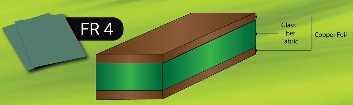
FR-4
FR-4 is a common material for printed circuit boards (PCBs). A thin layer of copper foil is typically laminated to one or both sides of an FR-4 glass epoxy panel. These are commonly referred to as copper clad laminates. The copper thickness or copper weight can vary and so is specified separately.
Referance taken from bantom tools
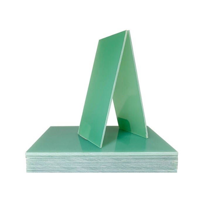
Garolite
G-10 or garolite is a high-pressure fiberglass laminate, a type of composite material.It is created by stacking multiple layers of glass cloth, soaked in epoxy resin, then compressing the resulting material under heat until the epoxy cures.It is manufactured in flat sheets, most often a few millimeters thick.
G-10 is very similar to Micarta and carbon fiber laminates, except that glass cloth is used as filler material. (Note that the professional nomenclature of "filler" and "matrix" in composite materials may be somewhat counterintuitive when applied to soaking textiles with resin.
G-10 is the toughest of the glass fiber resin laminates and therefore the most commonly used.
Referance taken from Wikipedia
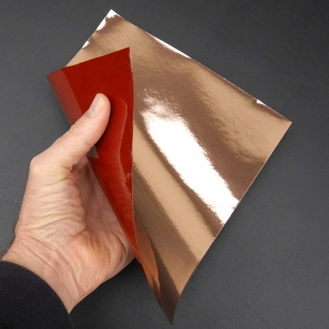
Flex Films
Flexible CCL refers to single-layer or double-layer flexible copper clad laminate made of PI film or polyester film as substrate material that are insulating and thin copper foil conductor with flexibility on surface. Compared with rigid CCL, it features light weight, thinness and flexibility so flexible PCBs with flexible CCL as substrate material are expansively applied in numerous electronic products including cell phone, digital camera, automotive GPS, laptop etc.
Referance taken from PCB Cart
Types of PCB Components
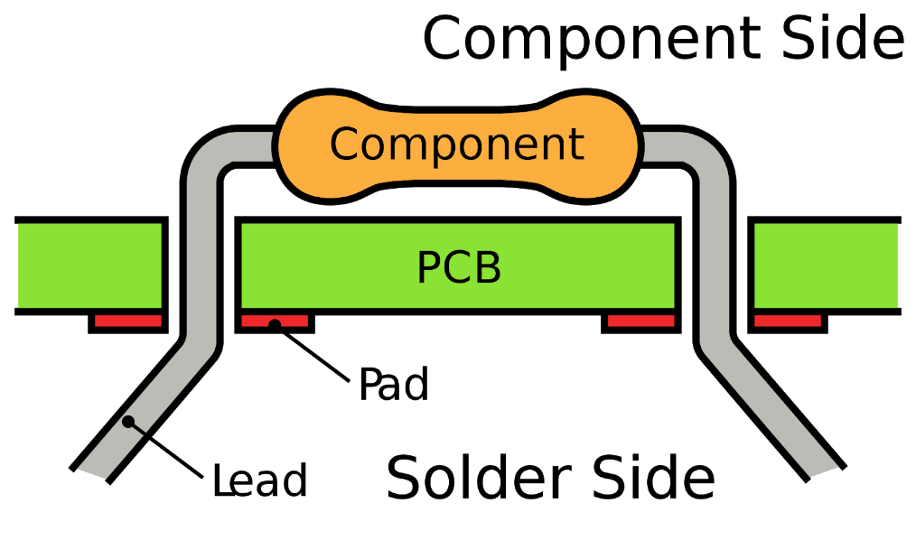
Throught Hole
Through holes on a PCB refer to a hole that is drilled from the top and through to the bottom of a PCB, these can be plated (PTH) or non-plated (NPTH).
Through-hole technology, also spelled “thru-hole”, refers to the mounting scheme used for electronic components that involves the use of leads on the components that are inserted into holes drilled in PCBs and soldered to pads on the opposite side either by manual assembly (hand placement) or by the use of automated insertion mount machines.
Through-hole technology almost completely replaced earlier electronics assembly techniques such as wire wrapping. From the second generation of computers in the 1950s until surface-mount-technology (SMT) became popular in the late 1980s, every component on a typical PCB was a through-hole component.
Referance Taken from EURO Circuits
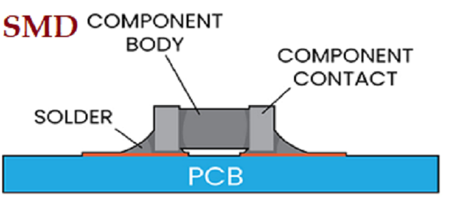
Surface Mount
Surface-mount technology (SMT), originally called planar mounting,[1] is a method in which the electrical components are mounted directly onto the surface of a printed circuit board (PCB).[2] An electrical component mounted in this manner is referred to as a surface-mount device (SMD). In industry, this approach has largely replaced the through-hole technology construction method of fitting components, in large part because SMT allows for increased manufacturing automation which reduces cost and improves quality.[3] It also allows for more components to fit on a given area of substrate. Both technologies can be used on the same board, with the through-hole technology often used for components not suitable for surface mounting such as large transformers and heat-sinked power semiconductors.
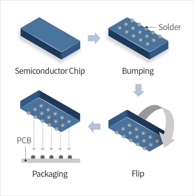
Chip Scale
A chip scale package or chip-scale package (CSP) is a type of integrated circuit package.
Originally, CSP was the acronym for chip-size packaging. Since only a few packages are chip size, the meaning of the acronym was adapted to chip-scale packaging. According to IPC's standard J-STD-012, Implementation of Flip Chip and Chip Scale Technology, in order to qualify as chip scale, the package must have an area no greater than 1.2 times that of the die and it must be a single-die, direct surface mountable package. Another criterion that is often applied to qualify these packages as CSPs is their ball pitch should be no more than 1 mm.
Referance Taken from Wikipedia
assembly process
Soldering Process
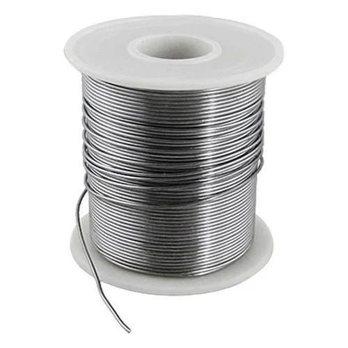
Soldering uses a filler metal with a low melting point, also known as solder, to join metal surfaces. The solder is usually made up of an alloy consisting of tin and lead whose melting point is around 235°C and 350°C, respectively.
But when tin and lead are mixed then the melting point of the mixture is reduced to 183°C. The alloy is melted by using a hot iron at above 316 °C (600 °F).
As the solder cools, it creates a strong electrical and mechanical bond between the metal surfaces. The bond allows the metal parts to achieve electrical contact while it is held in place.
Note that lead-free solders are increasingly used as an alternative to environmentally harmful lead-based solders due to regulations.
Lead Based Solder
Lead solder is a mixture of 60% tin and 40% lead (or 63/37). It is popular thanks to its low melting point (183°C). They are easy to work with, flow well and form strong bonds with other metals. Lead-free solder formulations have a varied percentage of metals.
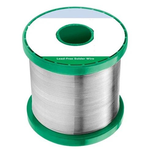
Lead Free Solder
Lead-free solder formulations have a varied percentage of metals. Components can include tin, copper, silver, nickel and zinc. The most common lead-free mix is tin-copper, which has a melting point of 217°C.
Solder Paste
- Solder paste is used in the manufacture of printed circuit boards to connect surface mount components to pads on the board. It is also possible to solder through-hole pin in paste components by printing solder paste in and over the holes. The sticky paste temporarily holds components in place; the board is then heated, melting the paste and forming a mechanical bond as well as an electrical connection. The paste is applied to the board by jet printing, stencil printing or syringe; then the components are put in place by a pick-and-place machine or by hand.
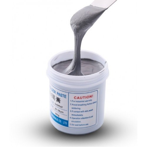
Referance Taken From Wikipedia
Desoldering
In electronics, desoldering is the removal of solder and components from a circuit board for troubleshooting, repair, replacement, and salvage.
Desoldering Braid
Desoldering braid, also known as desoldering wick or solder wick, is finely braided 18 to 42 AWG copper wire coated with rosin flux, usually supplied on a roll.
The end of a length of braid is placed over the soldered connections of a component being removed. The connections are heated with a soldering iron until the solder melts and is wicked into the braid by capillary action. The braid is removed while the solder is still molten, its used section cut off and discarded when cool. Short lengths of cut braid will prevent heat being carried away by the braid instead of heating the joint.
Desoldering Pump
A desoldering pump, colloquially known as a solder sucker, is a manually-operated device which is used to remove solder from a printed circuit board. There are two types: the plunger style and bulb style.[1] (An electrically-operated pump for this purpose would usually be called a vacuum pump.
Machine, Material @Fab Lab Vigyan Ashram
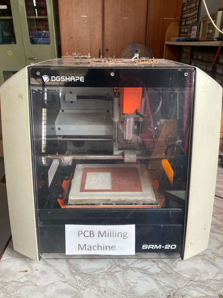
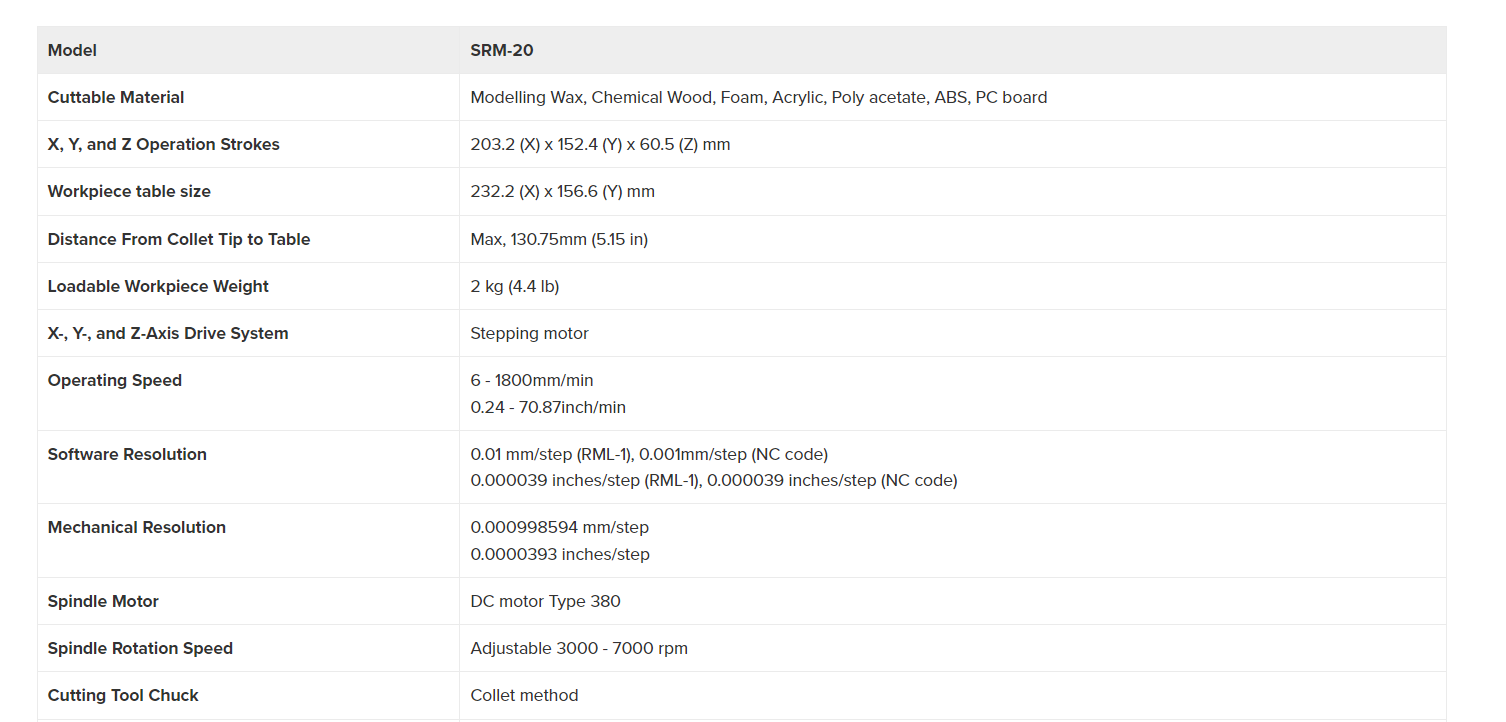
MonoFAB SRM-20
As a small milling machine, the SRM-20 offers compact size and powerful functionality at an affordable price. Production of realistic parts and prototypes is made simple and convenient with a device that fits into any office, studio, or classroom environment. For users looking for advanced milling capabilities without the need for expert operating skills, the SRM-20 is one of the easiest and most precise CNC mills in its class.
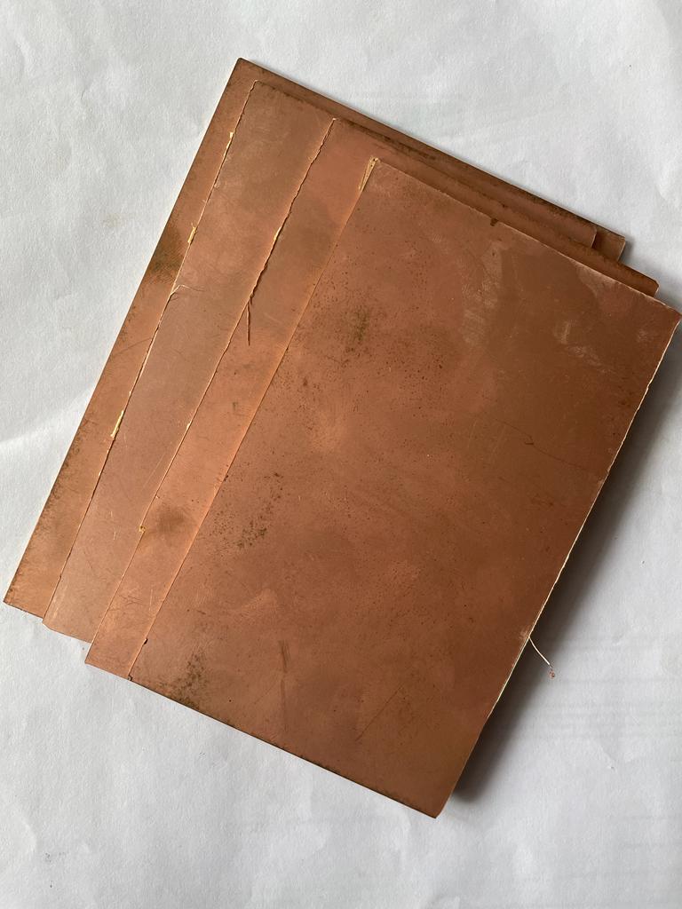
Material FR-01
FR-1 is a hard, flat material that consists of a thin layer of copper over a non-conductive phenolic resin. It’s usually about the thickness of two or three credit cards.
FR-1 is primarily used for making circuit boards. The thin copper layer can be milled or etched away, leaving traces to which electronic components can be soldered.
Unlike FR-4, which is fiberglass-based and generates dangerous glass-shard dust when milled, FR-1 is safe to use if you keep it away from your eyes, lungs, and skin. We recommend vacuuming up the debris after you’re done milling
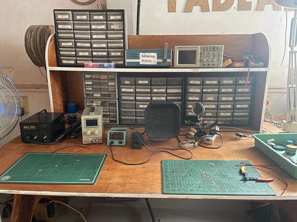
Soldering Station
Group Assignement
For this group assignment we have to calculate or check design rules for our PCB milling machine. For this we have used traces provided by Fab Academy.
Step 1- Machine
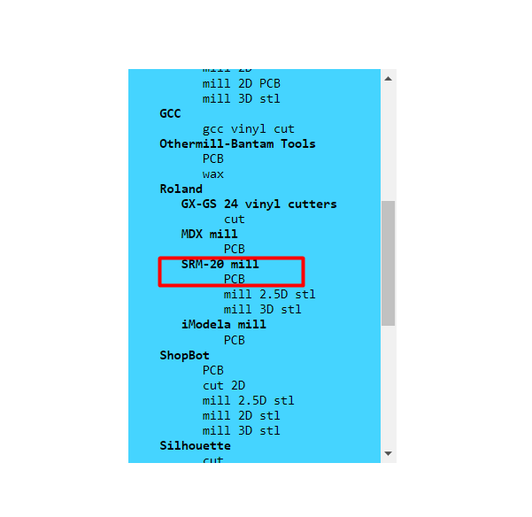
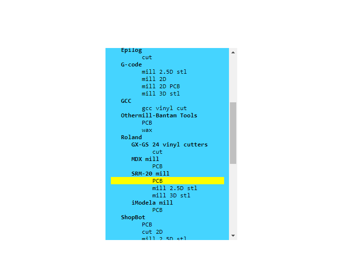
We have a monoFAB SRM 20 PCB milling machine at our @Fab lab Vigyan Ashram
Step 2- Design Sample
We have download the .png file of traces that we have to use for calibrating our machine, we have downloaded both the trace and outline files.


Mods
Used Mod For community by Fab academy to generate .rml file that can be used as input for machine software.
Selected machine and doing application under programs of mod community
After selecting machine and operation I did Uploaded a .png file into the mods.
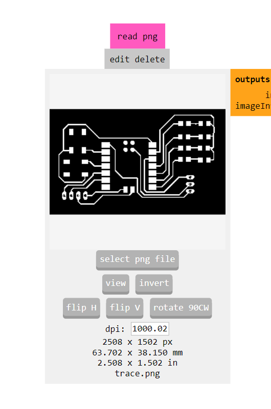
After uploading .png file, next process is tool selection, for making traces only we have to use 1/64 inch tool diameter and for through cutting we need to go for 1/32 tool diameter.
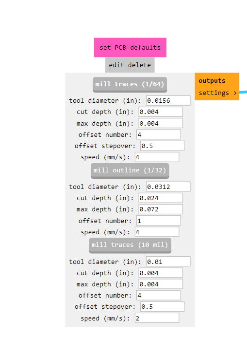
After setting up home position to 0, we can click on calculate button in-order to generate tool path for making traces or for through cutting process.
Machining
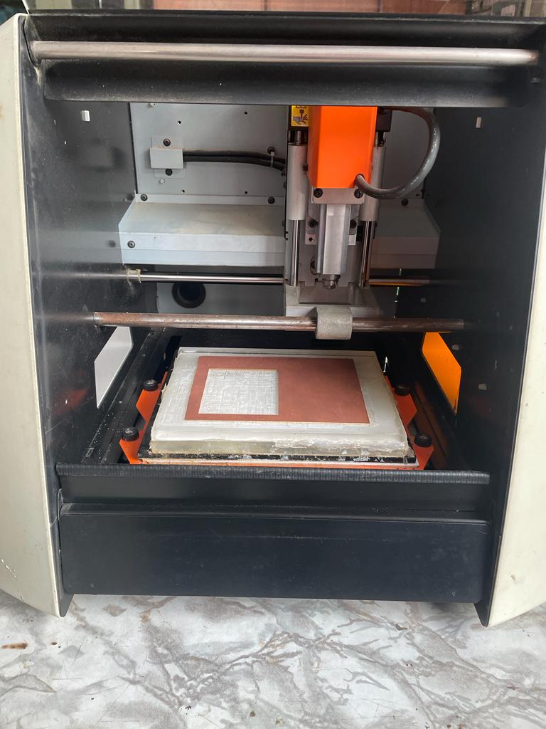
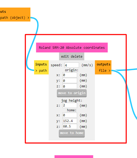
After completing all the process in to the mods, we got tool path in the form .rml file which actually used as input for machine software i.e Vpanel for SRM20.
After connecting machine to the local server we can operate milling machine through software.Highlighted buttons use to operate x,y and z axis of pcb milling machine.
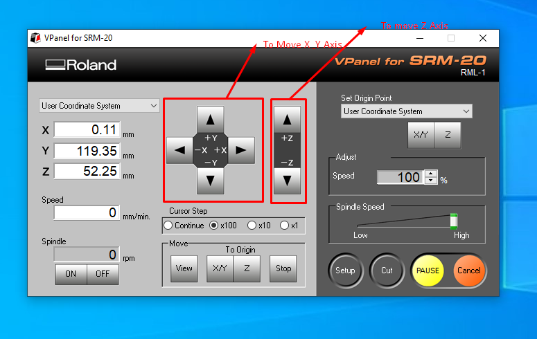
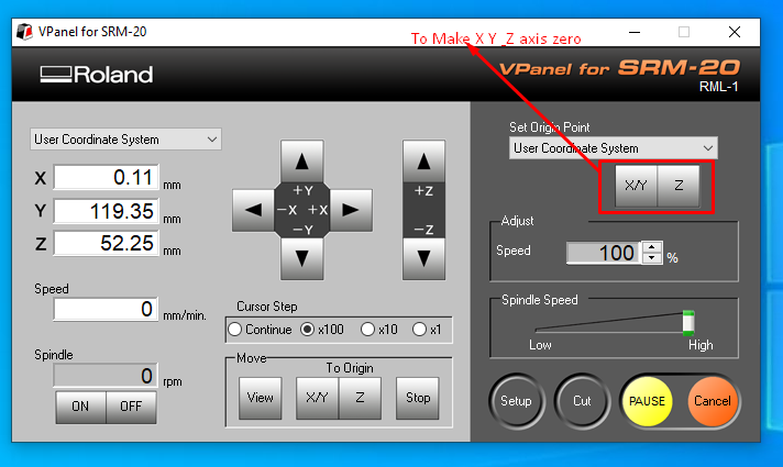
After setting x,y and z axis manually we did fix that position as a home position, through highlighted buttons we did that.
After doing all the initial machine setup work, we did uploaded. rml filr into the software and clicked on output button, and machine started doing it.
After completing all the machining process means making traces and cutting operation we got out final physical pcb.
Observation and conclsion of the assignement
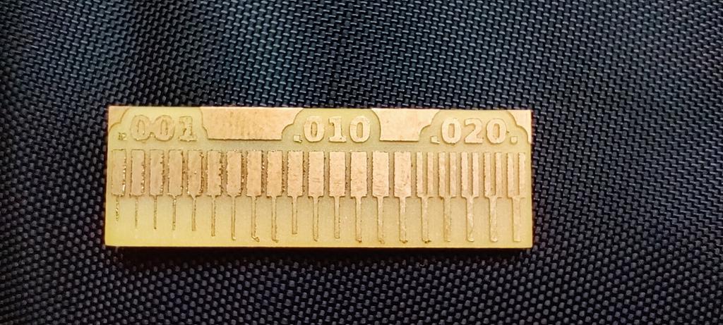
First - The width of traces sholud not be less than tool diameter. as we are using tool with 1/64 inch diamater and we can clearly able to see that traces are not cut properl where the trace width is less than tool diamater.
Second - Gap between any two traces are must be greater than tool diameter, as cam software will not generate tool path for such designs.
Individual Assignment
For the individual assignment we had a task to actually go for milling process that we have designed last week, last week I did design process with xiao esp32 c3 micro-controller but unfortunately it is not available in local market, so I revised my design and start making design with xiao rp2040 micro-controller.
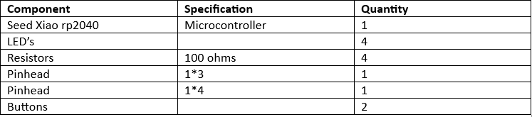
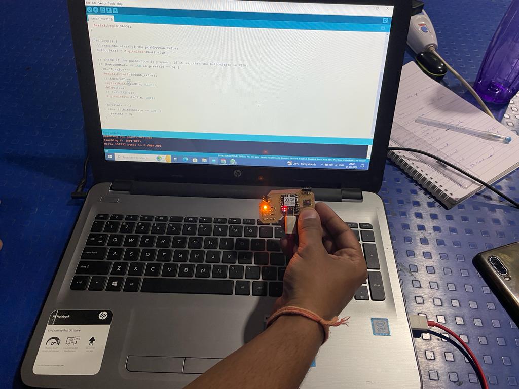
For the individual assignment I design, produce and program to develop a board that can blinks different LED’ s using push buttons.
Step 1 - Design with Autodesk Eagle
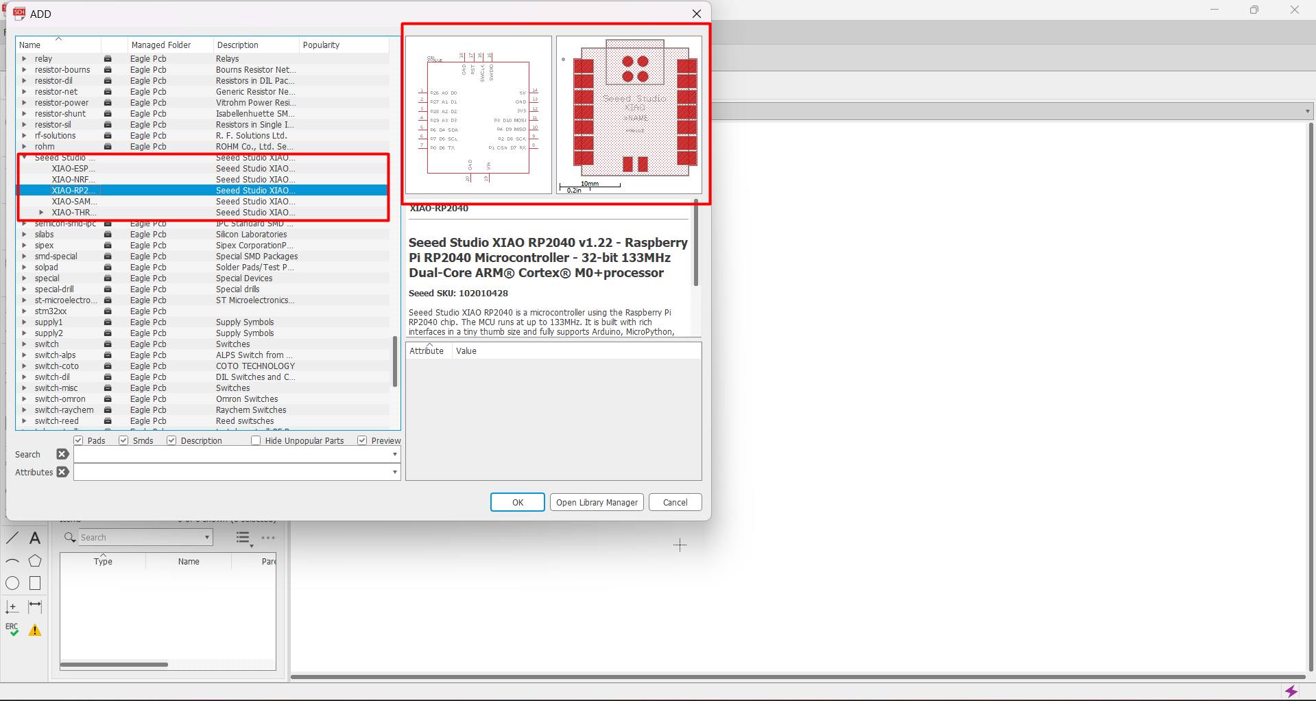
I have already uploaded library for seed studio xiao boards, so I directly started to add all the components that I require for designing a microcontroller board.
Additing xiao RP2040 micro-controllerfrom xiao library.
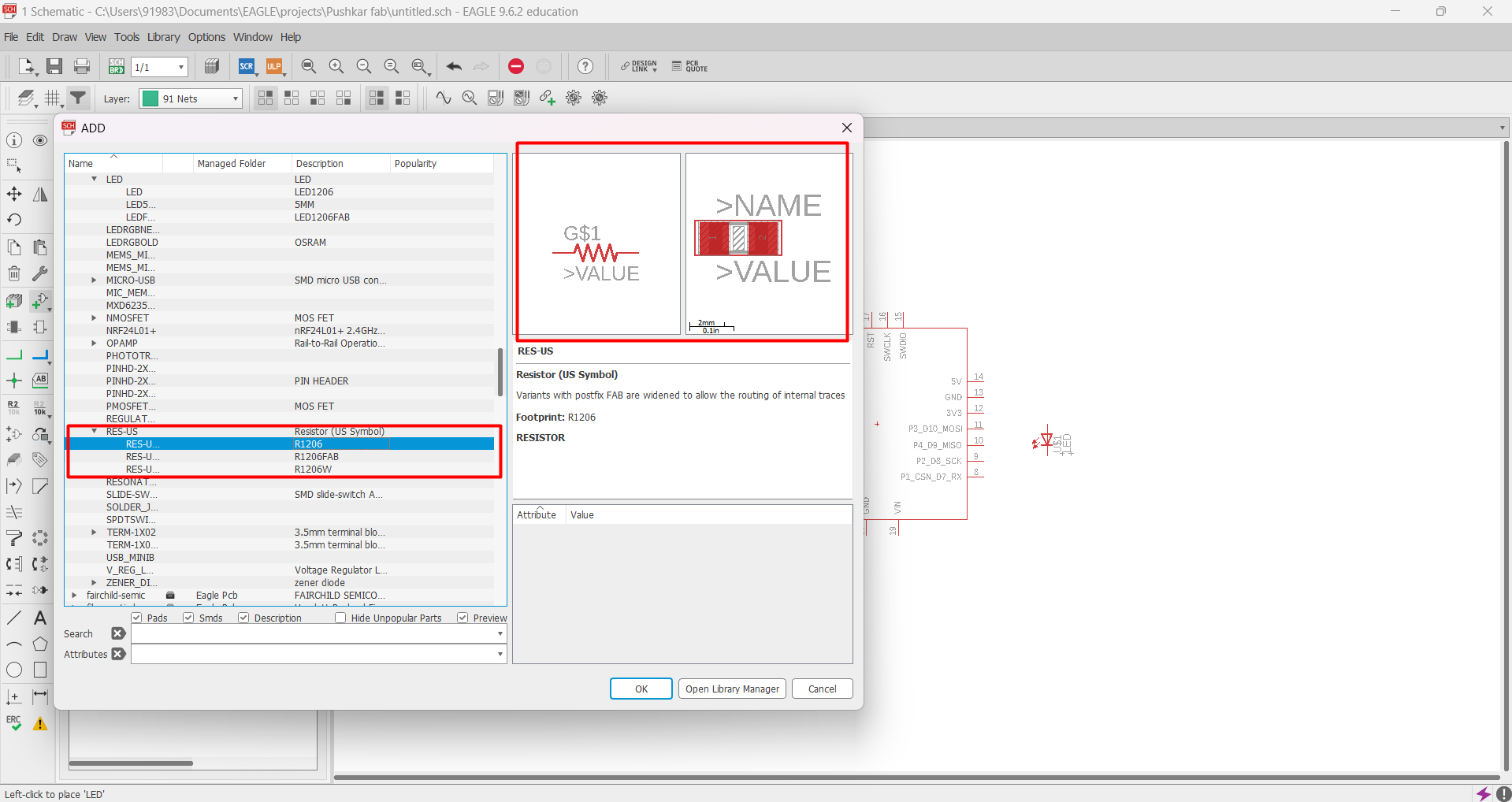
Added 4 LED's for Fab library.
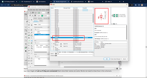
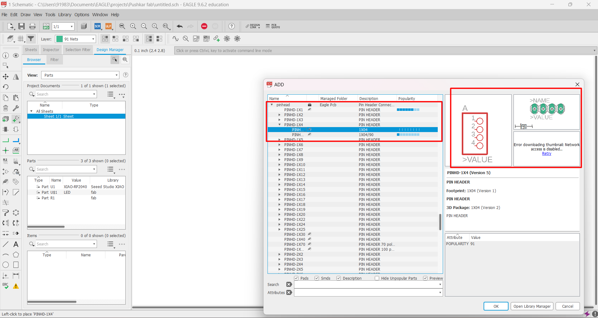
Added 1*4 pinhead for eagle library.
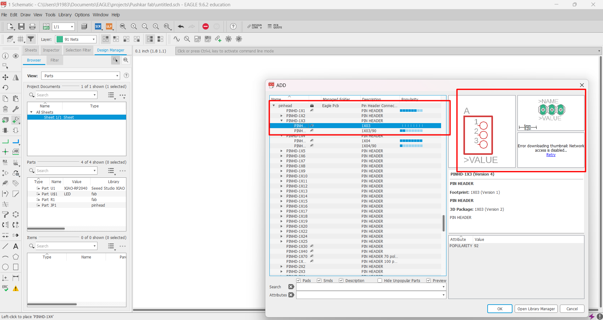
Added 1*3 pinhead for eagle library.
Added 4 quantity of 100ohm resistors from fab library.
After adding all the components I did manage to connect them to each other as per my requirement..
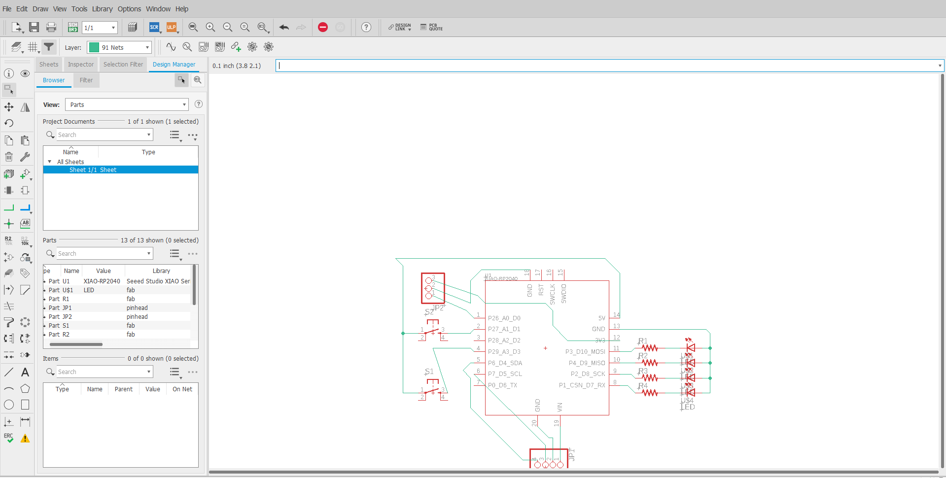
In-order to check errors inside my connection, I did ERC check for my design.
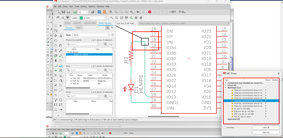
After removing all the errors showed up during ERC check, I did completed routing of my design to generate board.
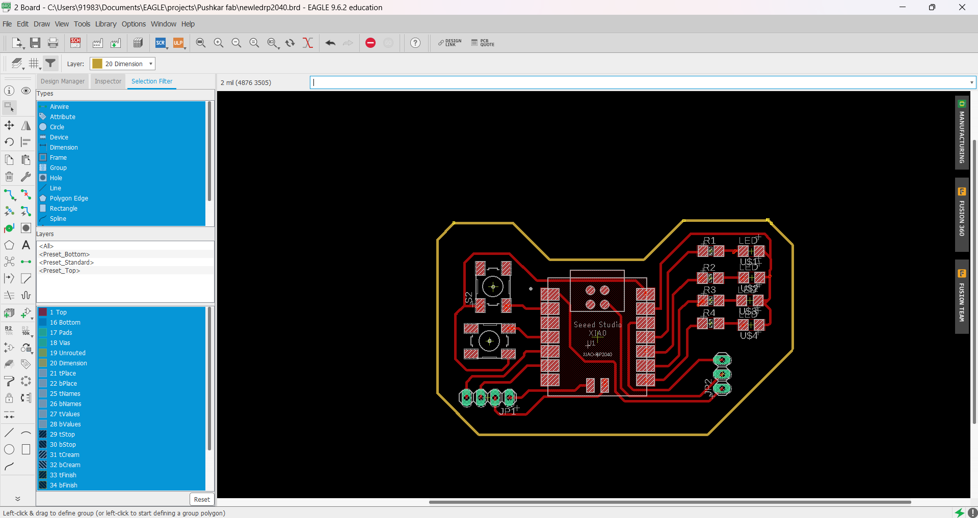
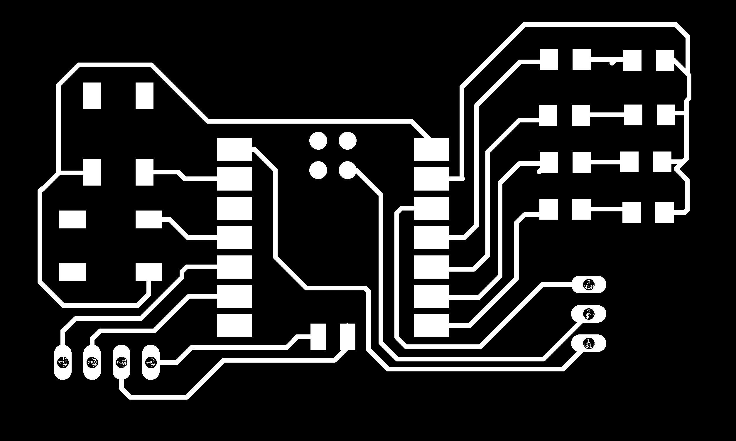
After completing my DRC check, I downloaded .png file of both traces and border cut for my design..
Step 2- Cummunity Mods
In-order to generate tool path, I did some processes in community mods by fab academy.
By opening mods I did selected machine and process that I need. We have SRM20 PCB milling machine at our fab lab.
Next step, I uploaded my .png file of traces that I have designed in eagle..
After uploading .png file for my traces, I need to select tool diameter, for traces I used 1/64 inch tool diameter.
Then I have set up the value of origin to 0 for all the axis.
All completing above processes sucessfully, I clicked on calculate button and it automatically generates tool path in the form of .rml file for my traces..

I did the similar process for generating tool path for outside border, for that I want throughout cut so I selected tool diameter to 1/32 inch for cutting process.
Step 3- Cam Software
SRM20 milling machines used Vpanel SRM-20 cam software to operate machine.
Below image shows home layout for VPanel software.

Then I moved X, Y and Z axis of milling machine to fix new home position.
Fix the home position for all the axis.
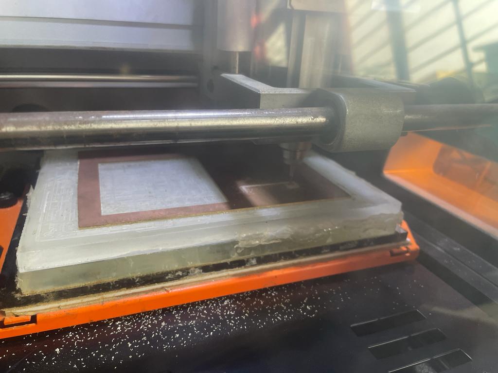
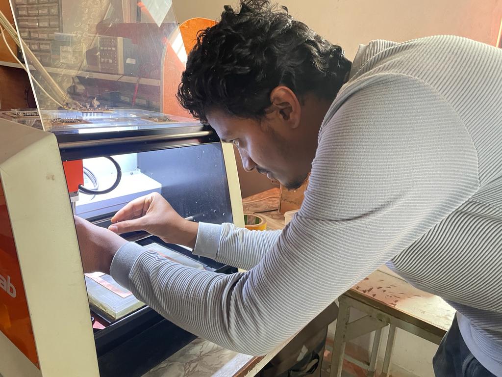
Step 4- Machining
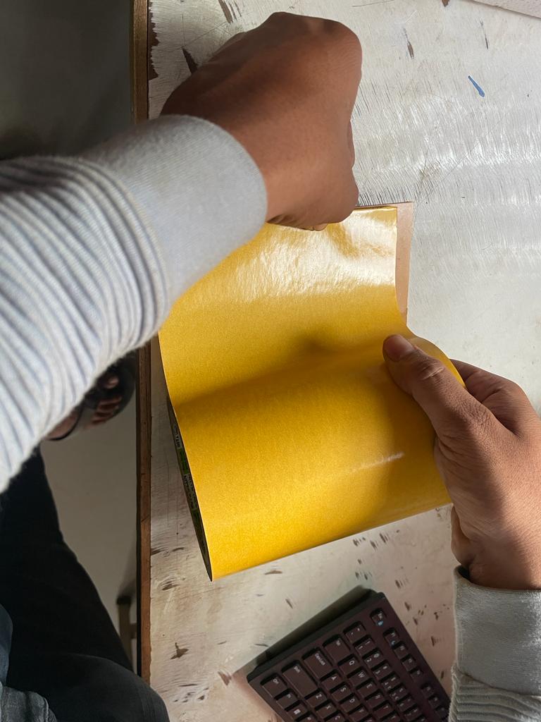
I have selected FR1 material for milling process as it is less hazardous than other materials.
Applied a double sided tape to the material to fix that material to the bed.
After fixing material I did fix the tool for making traces into it.
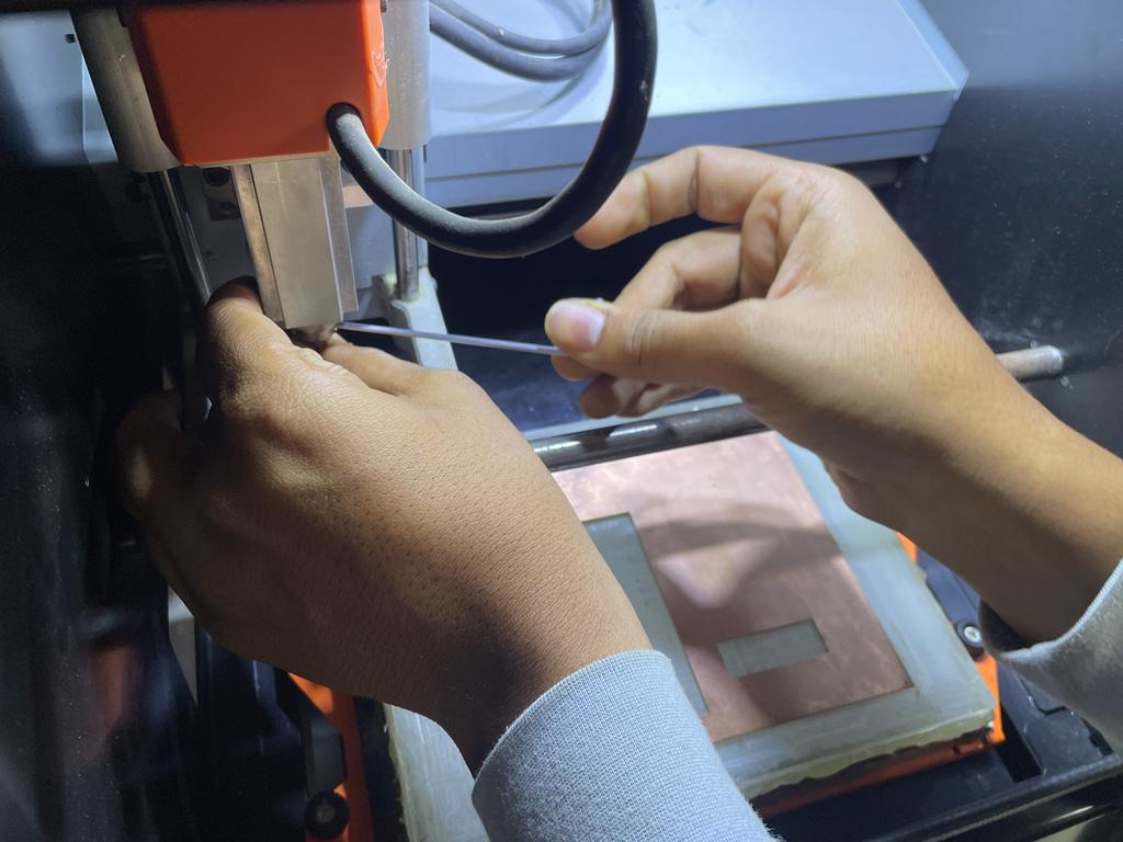
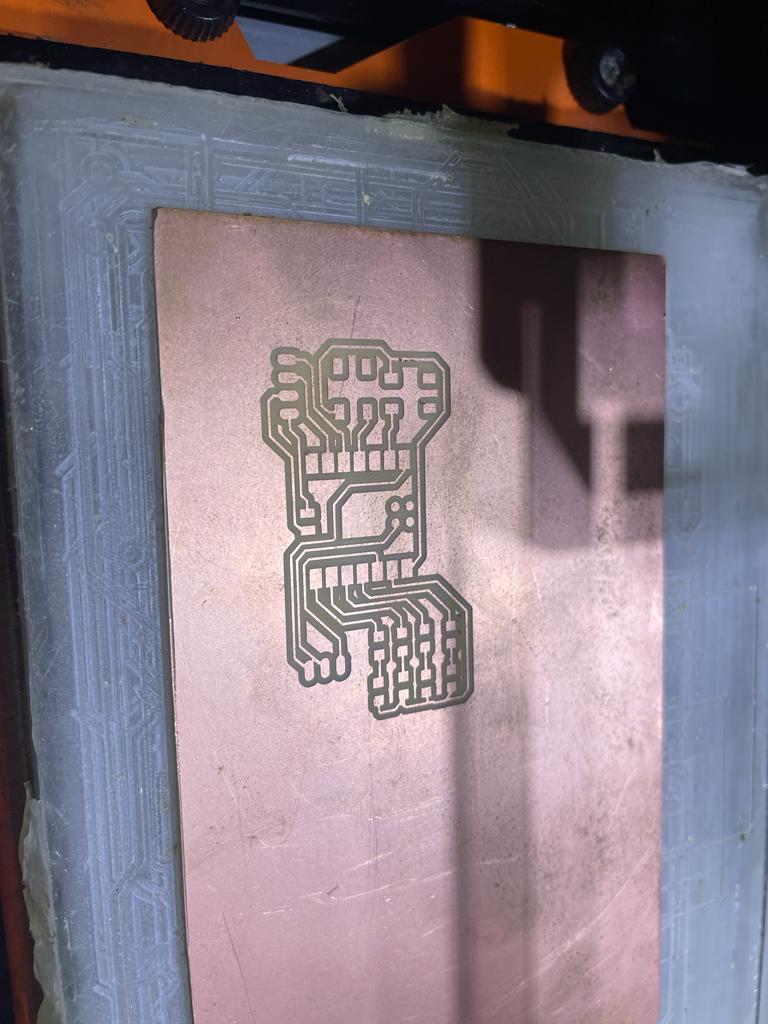
After machining process my traces were look like this, all things went well.
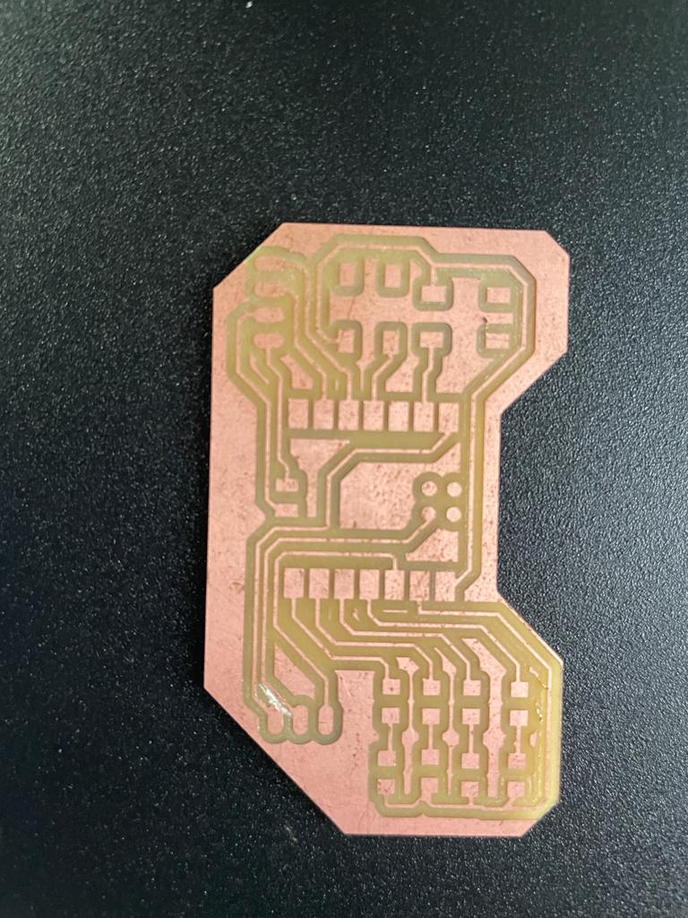
Then I did the similar process for the cutting also, for this process I changes the 1/64 inch tool with 1/32 inch tool.
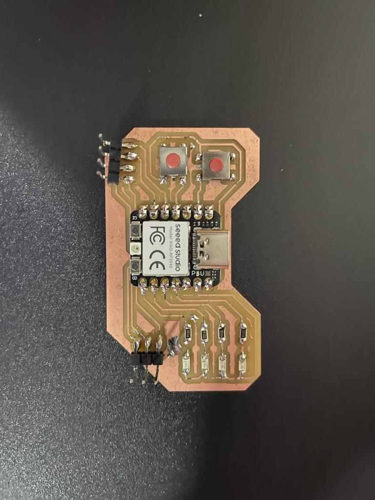
After completing machining process my final PCB is look like this.
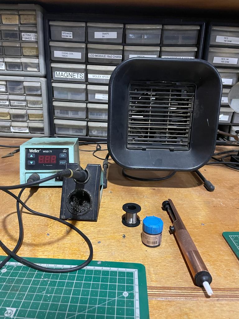
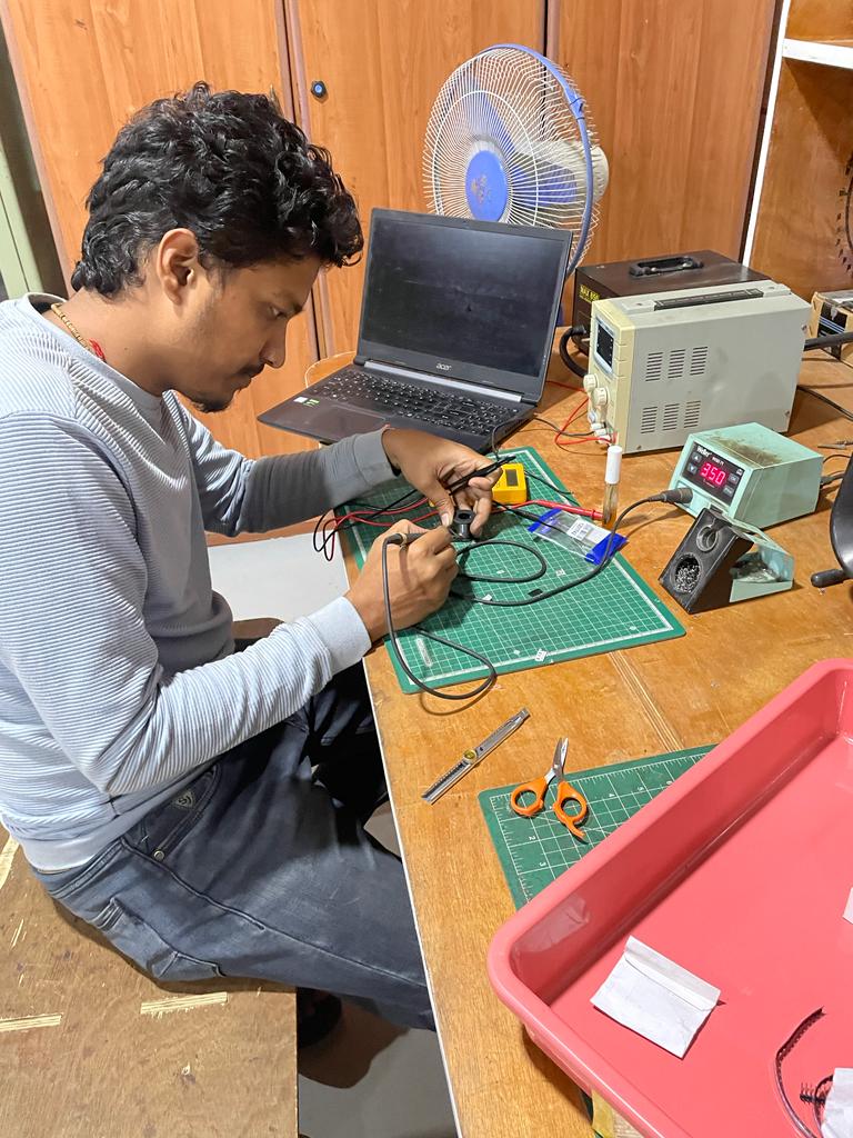
Step 5- Soldering Process
Collected all the components and started soldering it, we have soldering machine SMD components.
These soldering equipments that I have used for soldering my components.
Started soldering it considering proper soldering methods, i.e inside to outside and from small size components to large size components.Started soldering with LED& resistors and then added micro-controller and lastly added pinheads and buttons.
After soldering all the components to the board my final PCB is look like this.
Step 6- Pragramming
Xiao rp2040 works with C/C++, FreePascal, Rust, Go, MicroPython, and CircuitPython. So I have tried to work with c++ using Arduino IDE.
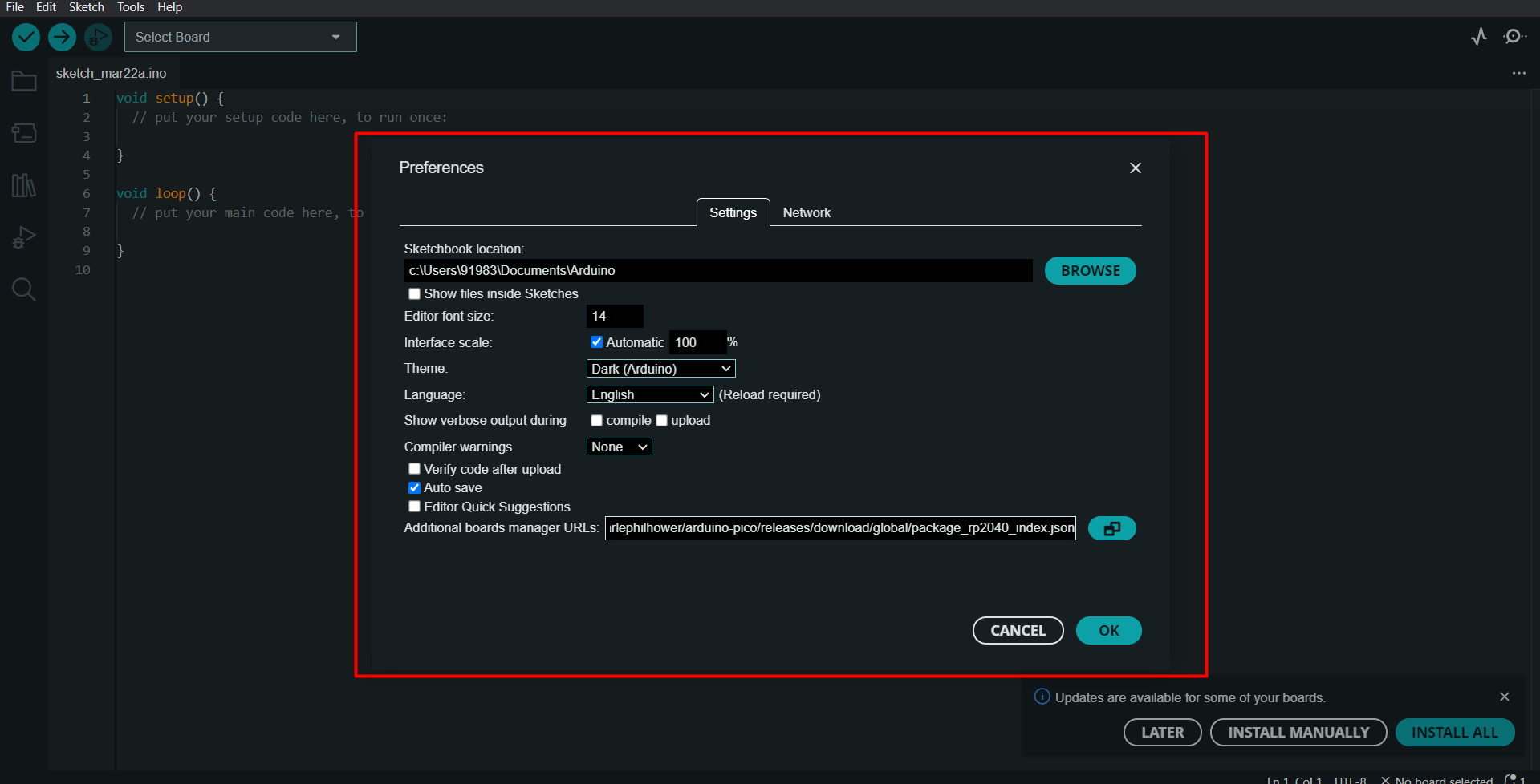
Downloaded a board management URL from seedstudio site.
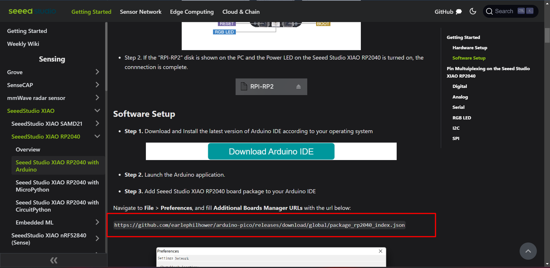
Pasted it to preference> additional board manager> install
First sample code to On/OFF led through button.
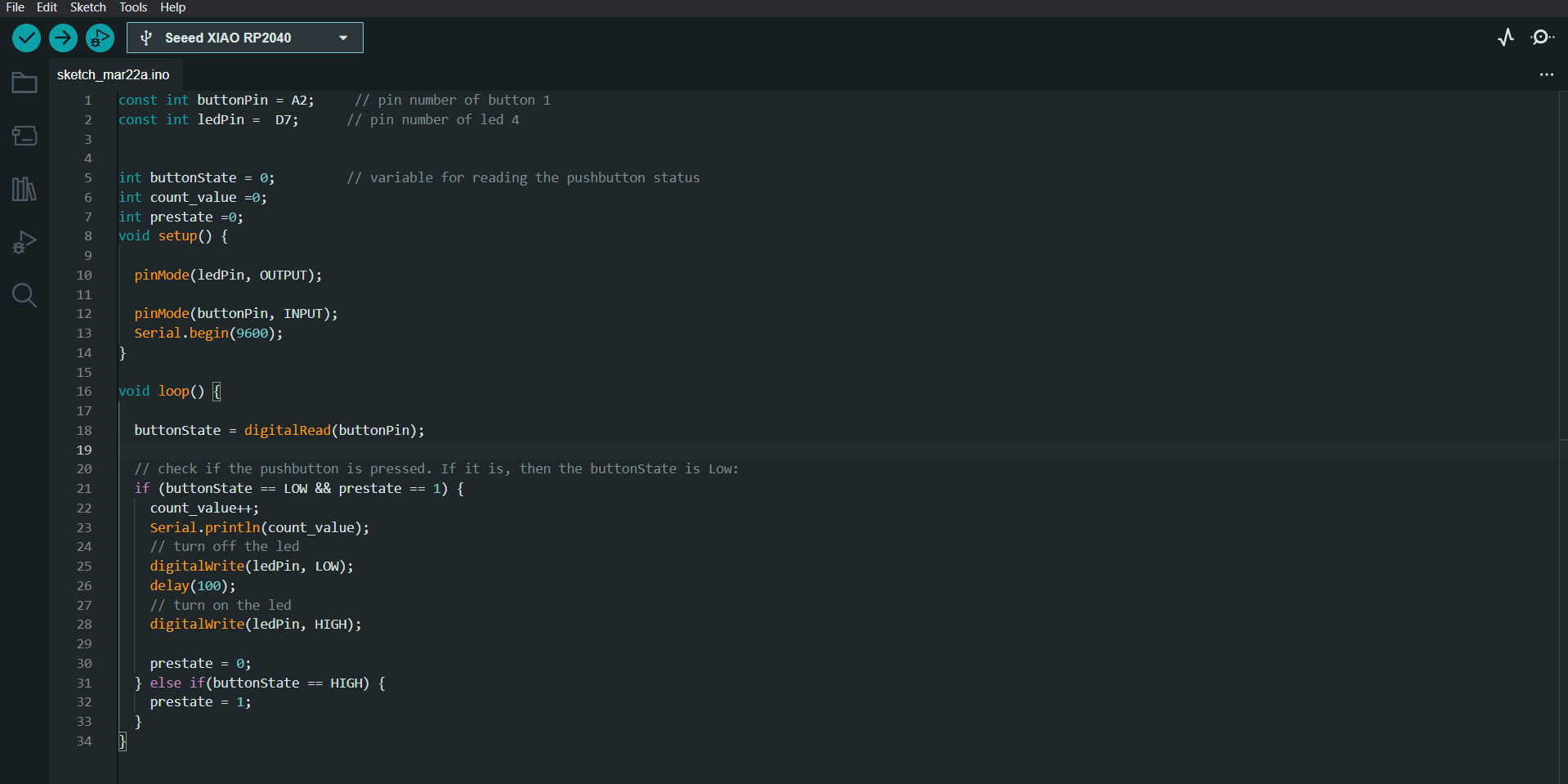
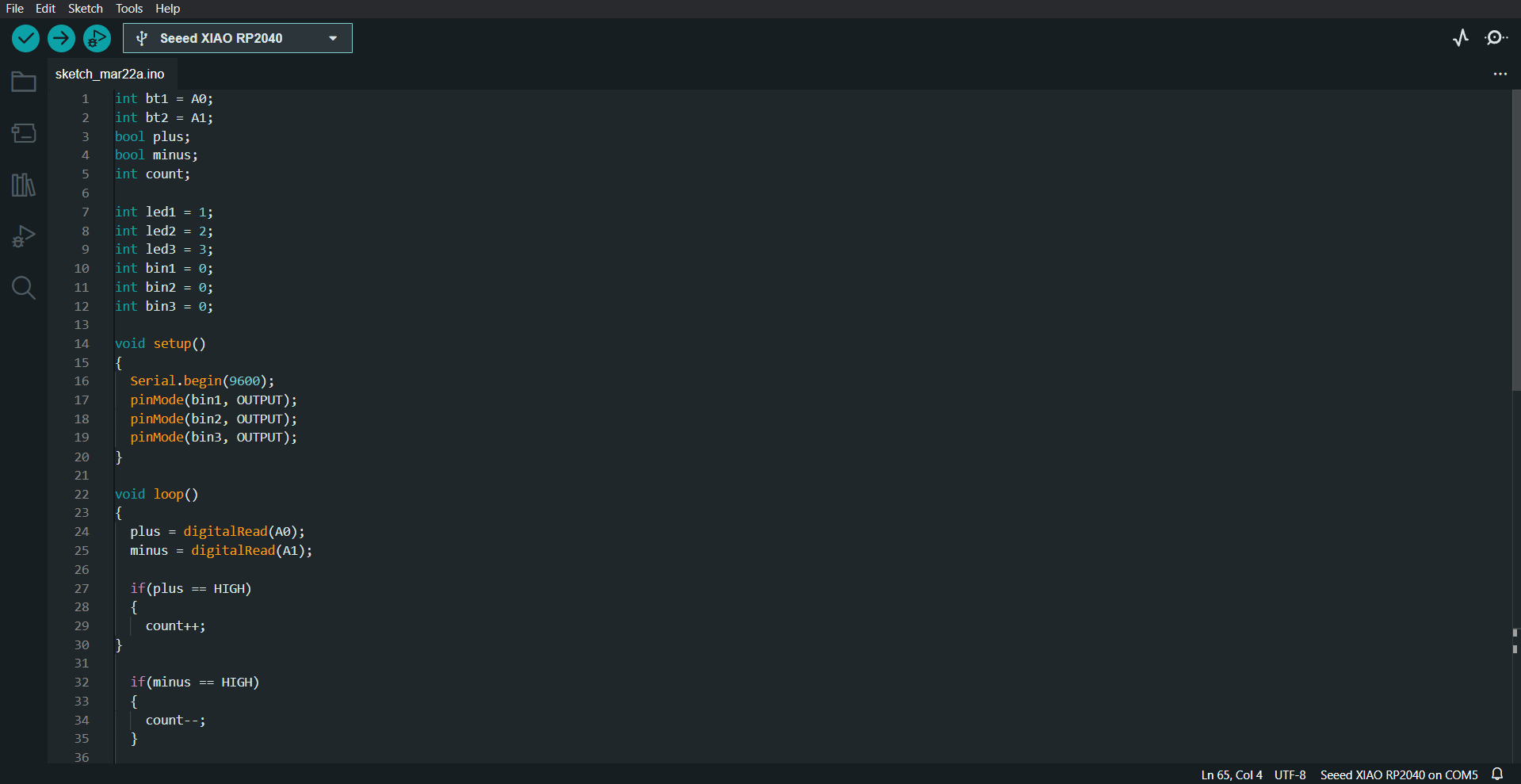
Controlling led blinking or making patterns using 2 different buttons.
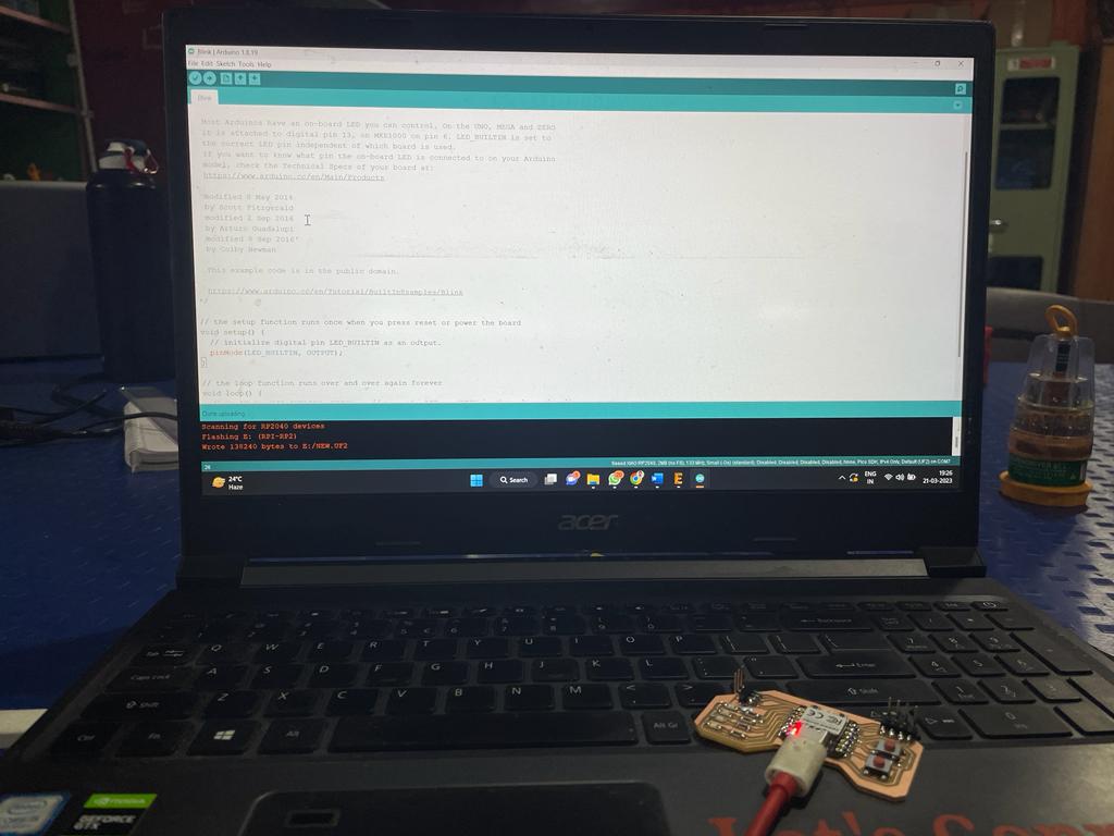
Testing code to blink buildin Led of RP2040.
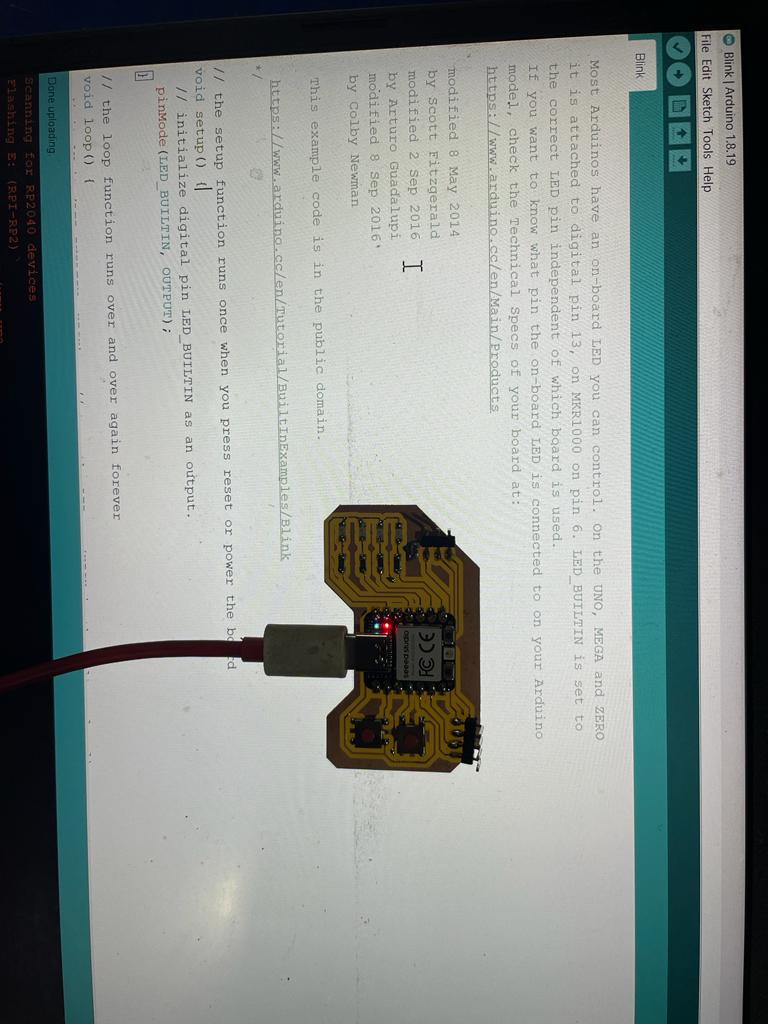
As seed xiao board support type C data cable for code uploading process.
Step 7- Final Output
Video
Learning from this week
1) Can able to use PCB Milling machine along with its machine software
2) able to do soldering of SMD Components
3) Become more familier with electronics
Problem Faced
Problem faced while making PCB compact - As my boards are equipd with lots of components, so initially it became so bulky and big. and if i try to make it smaller then i faced issue with overlapping of traces. Then spending hours on it finally i got solution to make it compact.
Milling bit 1/64 inch got broken - I fix new FR1 material sheet on the bed, and while milling it bit with size 1/64 inch got broken. i think that issues causes because of alignment of FR1 material withe bed. then i have changed the bit and got very good milling experience.