Electronics Production
Group Assignement
For this group assignment we have to calculate or check design rules for our PCB milling machine. For this we have used traces provided by Fab Academy.
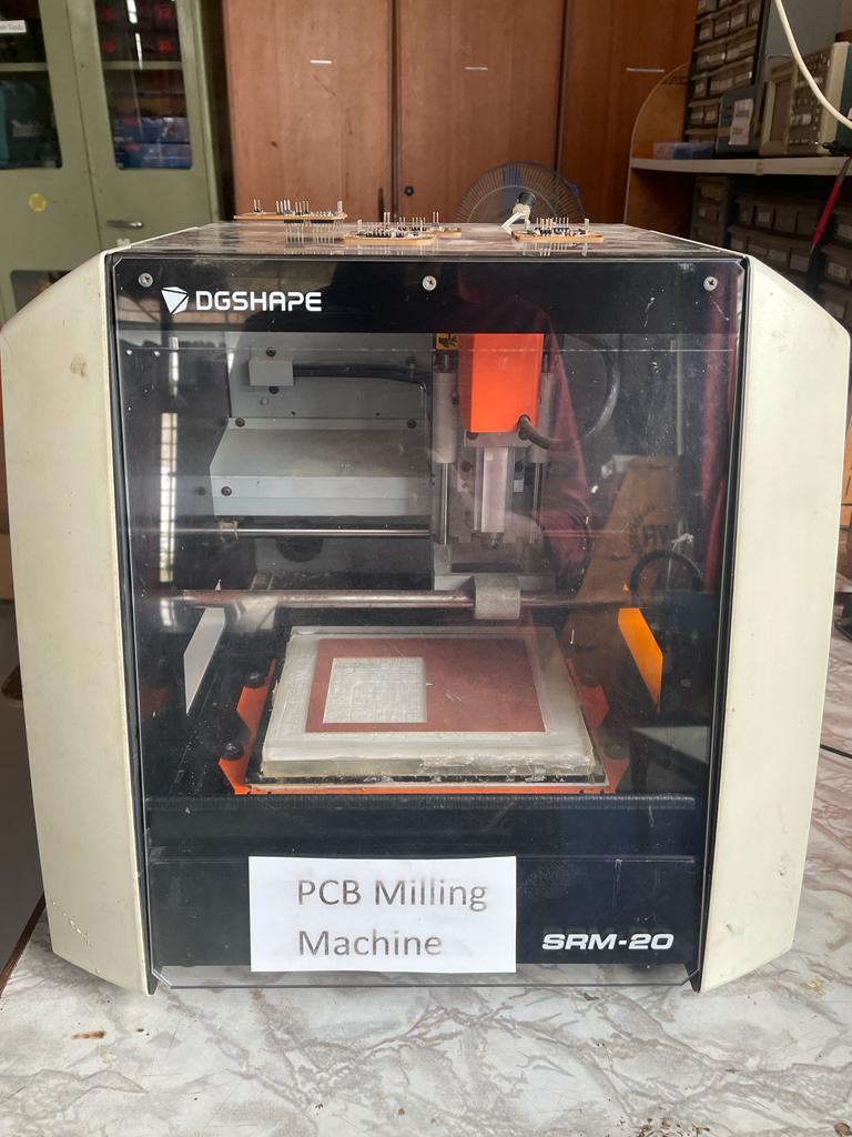
Step 1- Machine
We have a monoFAB SRM 20 PCB milling machine at our @Fab lab Vigyan Ashram
Step 2- Design Sample
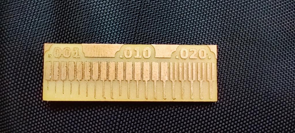
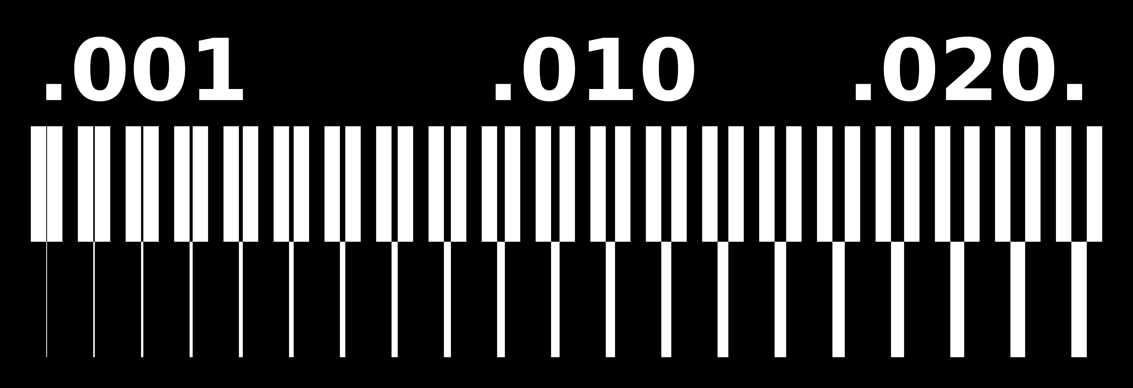
We have download the .png file of traces that we have to use for calibrating our machine, we have downloaded both the trace and outline files.

Mods
Used Mod For community by Fab academy to generate .rml file that can be used as input for machine software.
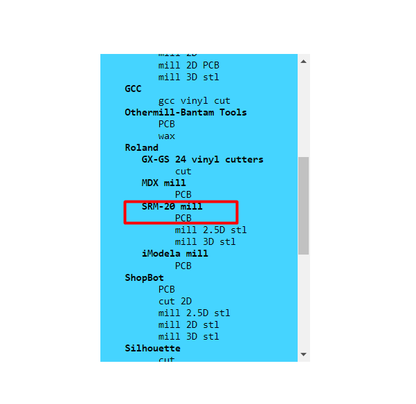
Selected machine and doing application under programs of mod community
After selecting machine and operation I did Uploaded a .png file into the mods.
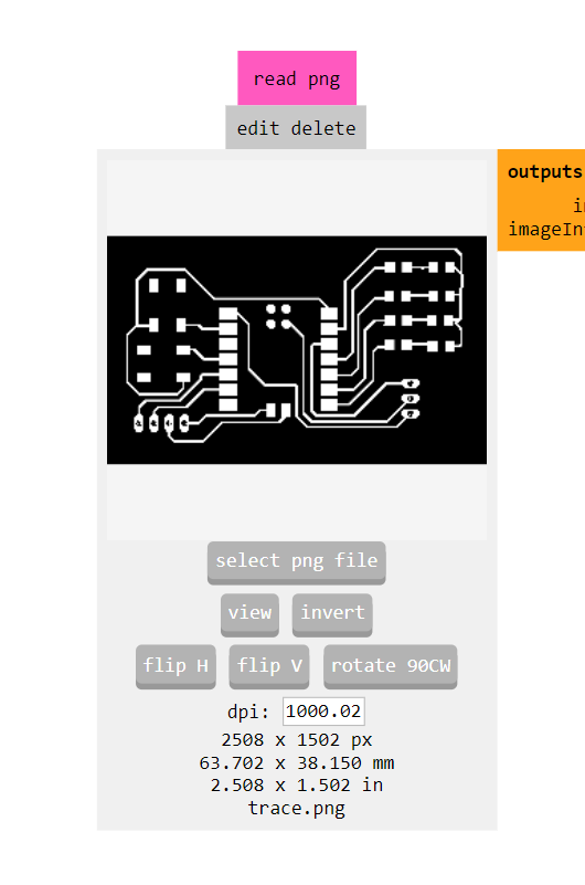
After uploading .png file, next process is tool selection, for making traces only we have to use 1/64 inch tool diameter and for through cutting we need to go for 1/32 tool diameter.
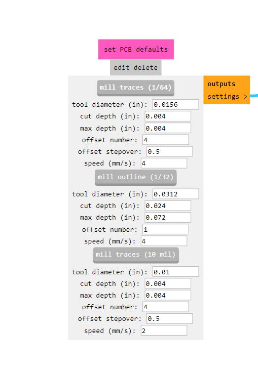
After setting up home position to 0, we can click on calculate button in-order to generate tool path for making traces or for through cutting process.
Machining
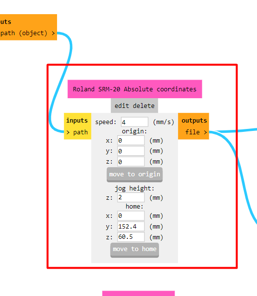
After completing all the process in to the mods, we got tool path in the form .rml file which actually used as input for machine software i.e Vpanel for SRM20.
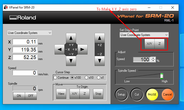
Home layout page of VPnael software.

After connecting machine to the local server we can operate milling machine through software.Highlighted buttons use to operate x,y and z axis of pcb milling machine.
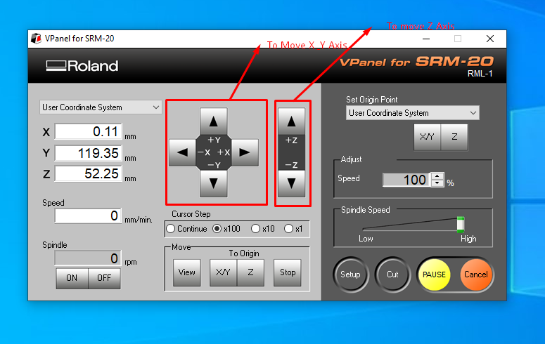
After setting x,y and z axis manually we did fix that position as a home position, through highlighted buttons we did that.
After doing all the initial machine setup work, we did uploaded. rml filr into the software and clicked on output button, and machine started doing it.
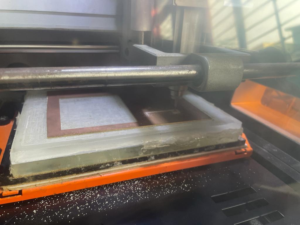
After completing all the machining process means making traces and cutting operation we got out final physical pcb.