
6.Electronics design
Group Assignment
During this week, I found it easy to comprehend circuit design software, as both KiCAD and Fusion 360 were user-friendly and intuitive. To improve my skills in electronics, I focused on learning how to design circuits from scratch. On the second day of the week, I realized that I needed to level up my skills to become proficient in electronic circuit design.
To begin my journey in electronics, I referred to various books and resources. One of the best books I came across, recommended by my batchmate, was "ABC Basic connections. " The book contained detailed diagrams of different connection diagrams for various MCUs and microcontrollers. Using this book, I was able to comprehend the pin-out and pin input of microcontrollers, such as RXD, TXD pins, and so on.
This week, we have been focusing on the ATtiny412 microchip and were tasked with creating a hello board based on it. To get started, I familiarized myself with the chip and its specifications. Our instructors provided us with some design rules to follow, as some of us were new to milling PCBs.
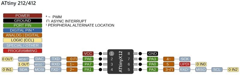
Getting familiar with the microchip is an essential first step in designing and building electronic devices. By understanding the specifications and capabilities of the chip, you can design circuits that are optimized for its performance. Additionally, following design rules and best practices is important to ensure that the circuit functions as intended and is reliable.
Creating a hello board is an excellent way to apply your knowledge of microchip specifications and circuit design principles. By building and testing the board, you can gain practical experience and identify areas for improvement. With practice and dedication, you can become proficient in designing and building electronic devices using microcontrollers like the ATtiny412.
Electronics
To calculate the minimum resistance required to run an LED with a voltage rating of 1.8V connected to a voltage of 5V, we can use Ohm's Law, which states that resistance (R) is equal to voltage (V) divided by current (I). In this case, the voltage across the resistor will be 5V - 1.8V = 3.2V (the remaining voltage after subtracting the LED voltage drop).
Assuming that the typical forward current for the LED is around 20mA (0.02A), we can calculate the minimum resistance using Ohm's Law:
R = V/I
R = 3.2V / 0.02A
R ≈ 160 ohms
Therefore, the minimum resistance required to run the LED with a voltage rating of 1.8V connected to a 5V source is approximately 160 ohms.
So, I added a resistance of 370 ohms for safety for the 2 LEDs and 10k ohms for the switch as a pull-up resistor.
Fusion 360
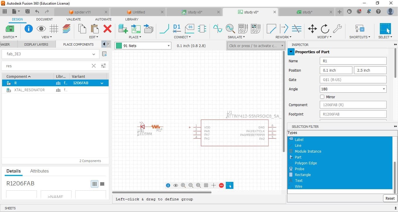
Fusion 360 is an incredibly useful and powerful software tool for designing PCBs. The auto-routing feature made it relatively easy to create PCB routes. Additionally, the library add-on was helpful in adding existing components from the fab library, making it easier to manage the design process.
However, one downside of using the fab library was that it did not have 3D models for the components. As a result, when the PCB was converted into 3D models, it remained a 2D model. Despite this limitation, Fusion 360 remains a valuable tool for designing PCBs, and there are ways to work around this issue by creating custom 3D models or sourcing them from other libraries.
Setup
1.To get started with fusion first we need to export the fab Lab library into fusion 360. To upload the library into fusion 360 first we need to,download the library. we just need to upload the library into the fusion and the library will be uploaded automatically
2.To start with a new PCB design first go to files<< new PCB design from there a new PCB design window appears and start a new PCB schematic
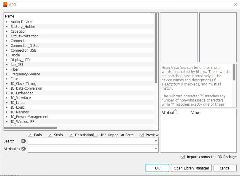
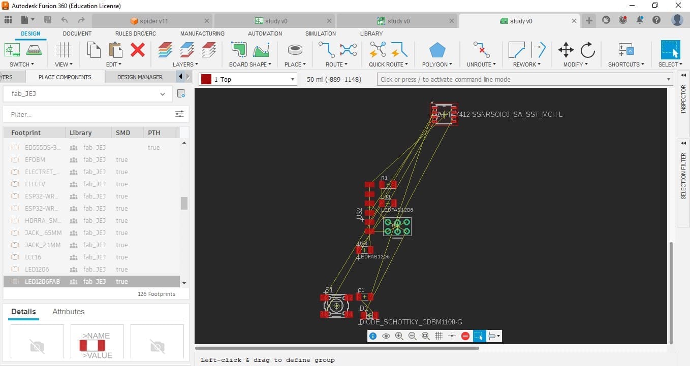
3.To add a component go to the library by going to the left side or press / to activate the terminal and type "Add". From the window add components by searching and double clicking them.
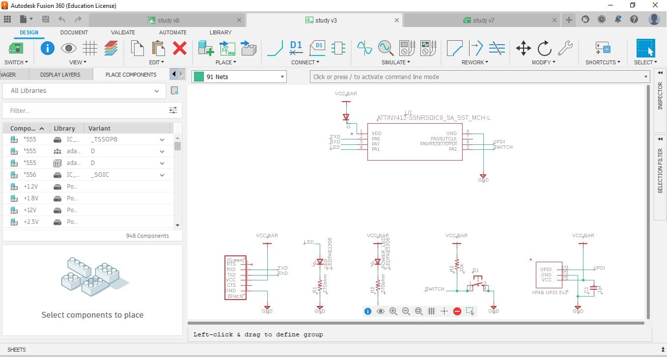
4.Add components into the layout diagram and give necessary connections.
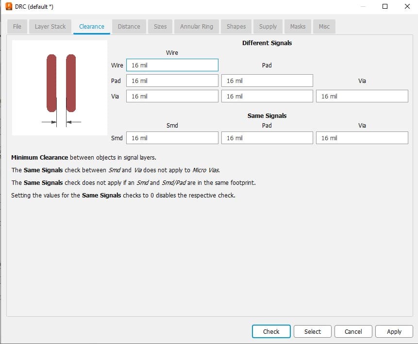
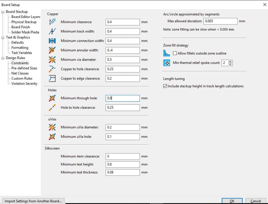
5.After the necessary connections are made go to validate and set your design rules. to do that go to switch to PCB document.
for us we have never used the design before, so the instructor told us to set the design rules as 16 mill because the minimum diameter of the milling machine is .4 mm so after setting the design rules click apply.
6.From here we can arrange the layout into a a block of certain size or we can create our own 2D board layout
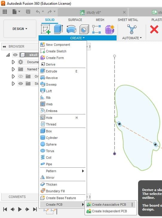
7.For me it was the image of a skull and I imported the SVG to fusion using import tool and arranged the the components inside the skull. I arranged the pins at mouth, led at the eyes and the switch at the nose. to link a 2D design to PCB go to create and link PCB. then we can go to the layout editor to edit our PCB.

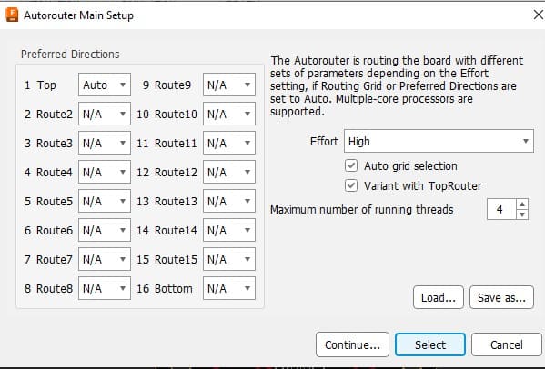
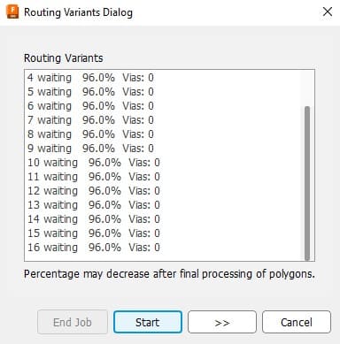
8.after the positions are set click on auto router under quick routes from there select the no of layers to be selected and select continue and start the routing.
after the design I did design a case if not my designing of the skull would have no purpose. unfortunately 3D models were not found so the things didn't go as I expected. Even though I completed the design of a case using my skull.
For me this week was more about being fun than being functional
DownloadPCB design files
KI CAD
DownloadKiCAD is a powerful EDA software suite that allows users to design electronic circuits and PCBs. It includes a range of tools for creating, editing, and reviewing schematics and PCB layouts, and automates the netlisting process to save time and reduce errors. Its PCB layout tool, Pcbnew, offers features such as automatic or manual routing, via stitching, copper pour, differential pair routing, and design rule checking. Users can also generate Gerber files and utilize 3D visualization tools to view the final PCB design in a three-dimensional environment, helping identify potential issues with layout or component placement.
One limitation of KiCAD compared to Fusion is that it does not include an autorouter, which is a tool that automatically routes traces between components. However, many users prefer manual routing as it allows for more control and can produce better results. Additionally, there are third-party autorouting plugins available for KiCAD.
Setup
1.To start designing in KICAD go to File>>New Project and a new schematic window will appear
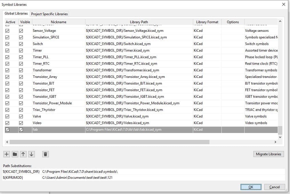
2.To start a design associated with Fab lab we need components from Fab lab and a library is required. I downloaded the library and by following the instructions the library was active and the fab components were active in my library.
3.From the window that appears we adding tools at the right hand side and visual tools at the top
4.Add components using "add symbol" tool and browse through the library to add symbols and to add power and ground select "add power symbols"
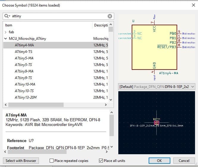
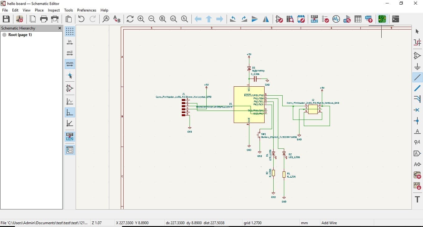
5.Add necessary components to the circuit and design according to the diagram for my case it was the hello board using Attiny-412 microcontroller.
While designing use shortcuts
M- To move
R- To rotate
W- For connection wire
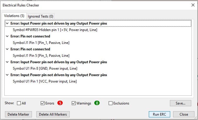
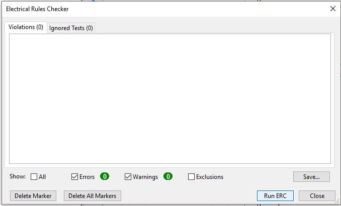
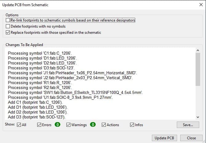
6.ERC- after completing the layout we need to run ERC to check the circuit diagram. In-order to do that go to ERC at the top right corner and from the window that appears click on RUN ERC and the errors will be displayed. In my case the errors were due to the lack of marking the unwanted pins and not adding power flags.
a.I needed to add power flags to a +5v and a GND to fix the errors
b. I needed to specify the non connected pins to do that go to Place<< Add no connect Flag and add the flag and my ERC errors were resolved.
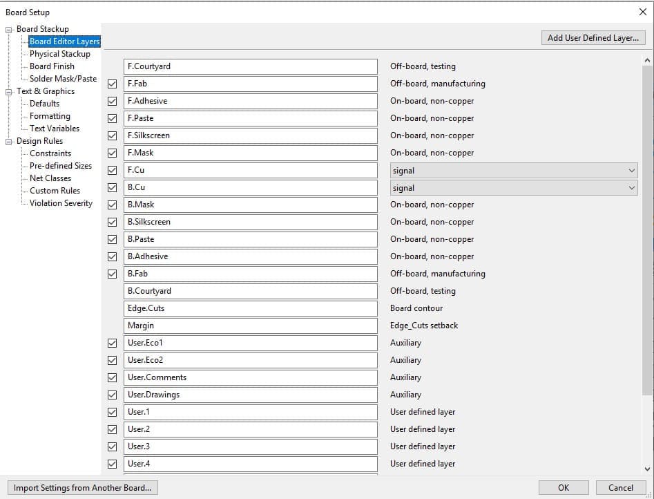
7.when the layout diagram is complete switch to PCB board editor by selecting the tool. when at the PCB board editor we need to select the design rules for the PCB such as no of layers and manufacturing rules, to do that go to "Design rules" at the left hand top corner and make the necessary changes. for this week the design rules is set as .4 mm which is the minimum dia of the tool as instructed as the instructor or 16 mill.
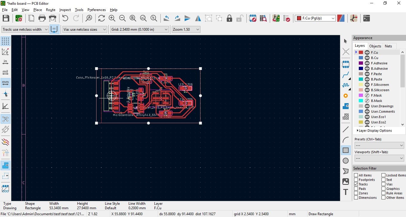
8.when at the PCB layout editor use move and rotate to position the components and make a circuit board shape. In my case I decided to go with a simple square design. And use route tracks to create tracks connecting the components.
In fusion we never had to do any hard work in routing, but in KICAD we need to find our own way across the components. We call it solving the MAZE
In KICAD we need to manually update the schematic design to PCB board editor to do that click on "update changes made with PCB " on the right hand top side and the schematics will be updated
9.DRC-After adjusting the maze we need to check for DRC for my case the errors I got was due to the shape of my board so I did a redesign of my board and some lines were not connected to the footer correctly so I just had to adjust the connections of the board.
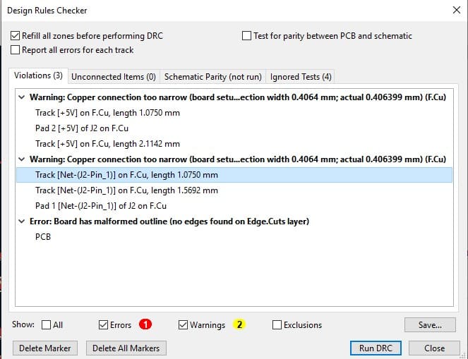
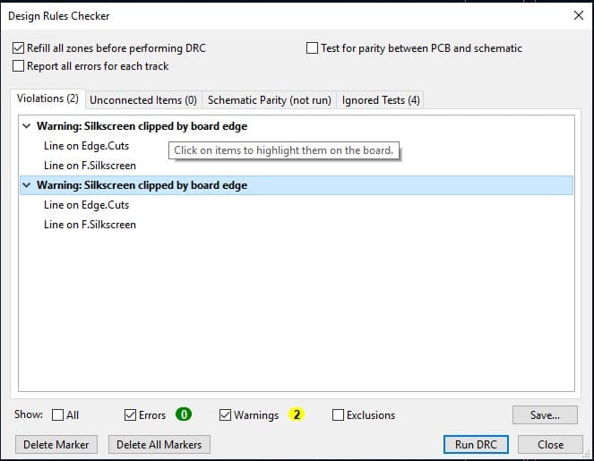
the later errors were because of my design and the pins were showing outside and it was within expectations so my errors were fixed.
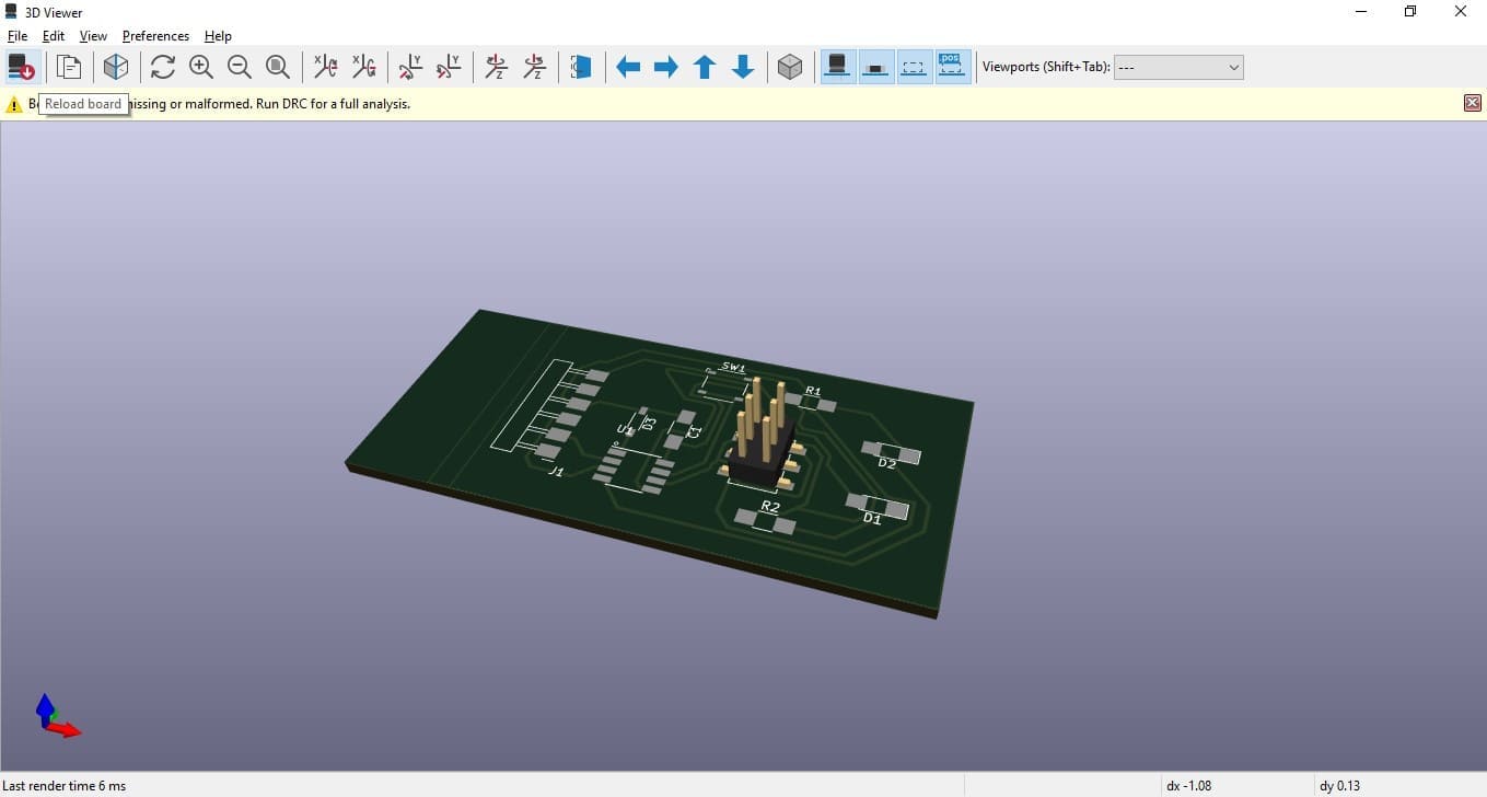
10.After completing the design to get a 3D view go to view<< 3D viewer and a 3D view of the board will be updated.
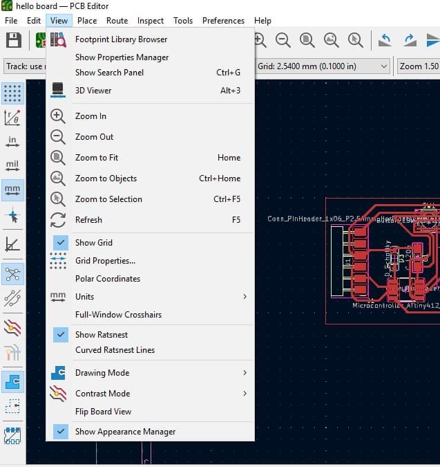
The 3D design is not still complete because it lacks 3D models for the components but an overall layout has been completed. And I can export the design as a .STEP file and create an associated design using fusion 360
Simulation
Simulating a circuit before manufacturing it has several advantages. Firstly, it allows us to test and verify the functionality of our circuit design without having to physically build it. This can save a significant amount of time and money, as we can identify and fix any issues or errors in the design before investing in the physical components. Secondly, simulation allows us to optimize the design by making changes and testing their effects without having to dismantle and rebuild the circuit each time. This means we can experiment with different configurations and components until we find the optimal solution that meets our needs. Thirdly, simulation can help us ensure that our circuit design is safe and reliable by identifying any potential issues or hazards before they occur. This is especially important in applications where safety is critical, such as medical devices or aerospace systems. Overall, simulating a circuit before manufacture is a valuable tool that can save time, money, and effort, while also helping us to optimize our design, ensure safety, and achieve the desired functionality.
wokwi
This week, I explored Wokwi simulation, which provides a web-based simulation platform for developer boards based on programming. With this tool, we can visually see the basic connections and outputs, such as high and low, to ensure that the connections are fully functional before actual manufacturing takes place. This can help prevent any potential errors or issues in the final product.
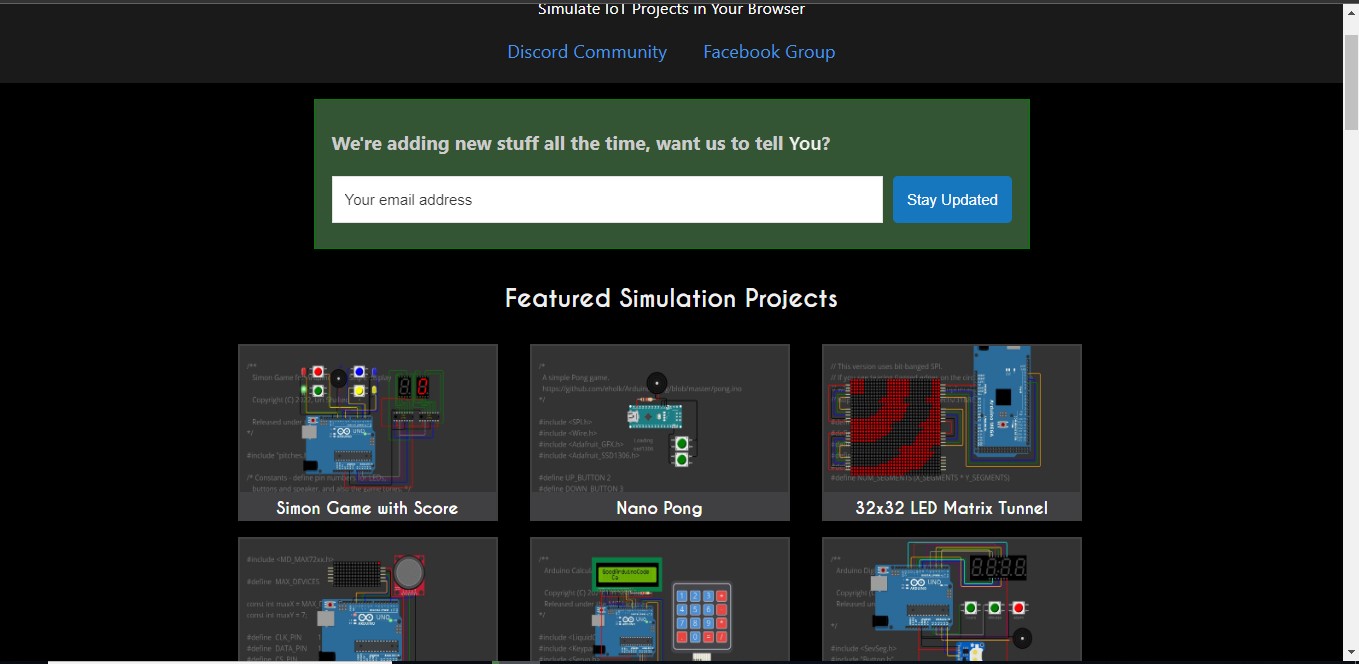
the interface and tools of Wokwi simulation are intentionally designed to be simple and easy to use, which makes it an ideal platform for anyone who is new to electronics and programming. Even children can use Wokwi to simulate basic electronic circuits, which makes it a great educational tool for introducing these concepts to beginners of all ages.
to get started first we need to select the dev board and make the necessary connections in my case I added a led with resistor and an input switch.
after selecting the board we can add led and resisters using the add button, we can move by selecting the part, rotate by pressing "R" and connect by clicking and dragging on ends. After that upload your code and press start simulation.