
Networking and communications
Group Assignment
For this week, my focus is on exploring communication protocols such as I2C and serial communication, as I believe they will be instrumental in my upcoming project. To achieve this, I plan to create an array of boards using the ATtiny412 chips, which I find both readily available and user-friendly. Furthermore, my previous experience with these chips during electronics design has given me a solid foundation to build upon. By leveraging the capabilities of the ATtiny412 chips and harnessing the power of I2C and serial communication, I aim to establish a network of interconnected boards that can seamlessly exchange data and collaborate on various tasks. This exploration of communication protocols and utilization of the ATtiny412 chips will undoubtedly open new possibilities and greatly contribute to the success of my project.
I2C Protocol
This week, my primary focus is to delve deeply into the intricacies of I2C and serial communication protocols as I recognize their immense value for my project. Specifically, I am determined to create an array of interconnected boards that seamlessly communicate utilizing these protocols. After careful consideration, I have decided to employ the ATtiny412 chips due to their wide availability and user-friendly nature, further bolstered by my previous experience with this chip during the electronics design and manufacturing week. With these factors in mind, I am eager to embark on the execution phase of my design, capitalizing on the capabilities of the ATtiny412 chips and harnessing the power of I2C and serial communication to establish a robust network of boards that can fluidly exchange data and collaborate harmoniously. This ambitious undertaking holds the promise of unlocking new horizons and amplifying the potential of my project, and I am excited to dedicate this week to its successful realization.

The figure above depicts a simplified representation of an I2C network, showcasing its key components and operation. In this network, there is a master device responsible for controlling the communication, while the other devices are designated as slaves. The master device grants permission for bidirectional data transfer between itself and the slaves. To facilitate this communication protocol, two essential pins are utilized: SDA (Serial Data) and SCL (Serial Clock). The SDA pin serves as the channel for transmitting data, while the SCL pin synchronizes the data transfer process by generating clock signals. Together, these pins enable seamless and reliable data exchange within the I2C network, with the master device governing the communication flow and authorizing bidirectional interaction. Understanding the role of the SDA and SCL pins, as well as the master-slave relationship, is crucial for implementing and leveraging the I2C communication protocol effectively, facilitating efficient data transfer and collaboration among the devices in the network.
Design
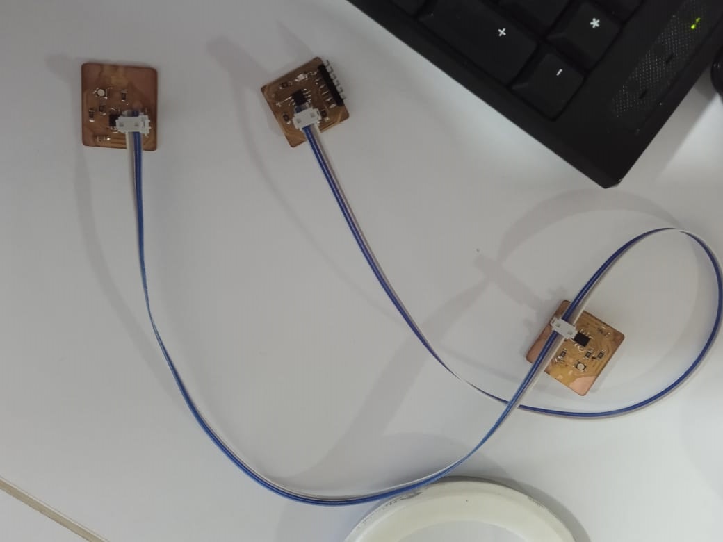
For this week, my primary focus is on creating a master board and two slave boards using the ATtiny412 microcontroller. To kickstart the design process, I began by developing the slave board, incorporating an RGB LED to provide versatile visual output with various color combinations and effects. Turning my attention to the master board, I strategically included serial communication pins to enable data exchange between the master and slave boards. Additionally, I integrated an internal LED on the master board, serving as a convenient indicator for circuit functionality verification during testing and troubleshooting. This systematic approach of sequentially designing the slave and master boards allows me to build upon each component's functionality, gradually advancing towards my project goals. Moving forward, I am excited to continue enhancing the design, integrating additional features, and harnessing the full potential of the ATtiny412 microcontroller to establish a robust and efficient communication system between the master and slave boards.
The milling process for this particular project proved to be relatively straightforward and yielded excellent results, devoid of any defects. Notably, we made an improvement by changing the milling bit, resulting in a higher resolution outcome compared to our previous attempts. This adjustment allowed for finer details and more precise cuts, enhancing the overall quality of the milled components. The ease with which we executed the milling process can be attributed to our past experiences and familiarity with similar projects. Leveraging our accumulated knowledge and skills, we approached the milling task with confidence and proficiency, resulting in a smooth and successful operation.

One interesting observation during the project was that the size of the master board turned out to be smaller than that of the slave boards. While this detail may seem trivial, it did elicit a sense of amusement. The comical notion of the "Puny Master" emerged as a lighthearted jest, highlighting the unexpected size discrepancy between the master and slave boards.
Once the manufacturing phase was completed, the focus shifted to debugging the boards. During the design process, it was important to cross-check some of the adopted designs, which may have been sourced from external references. To address this, I began by burning the bootloader to the slave boards, prioritizing their debugging. This step ensured a smooth programming process and provided a solid foundation for further testing. Next, I programmed the chips and implemented a simple LED blinking program to verify their functionality. Witnessing the expected LED blinking confirmed that the microcontroller chips were working as intended. This systematic debugging approach allowed for early detection and resolution of any potential issues, establishing confidence in the design and manufacturing process. With the successful debugging of the slave boards, I laid a solid groundwork for subsequent testing and development, ensuring the project's steady progress.
Regarding the master board, the initial step in its debugging process involved running a program to verify the functionality of the LED. Confirming that the LED was indeed blinking as intended served as an encouraging sign, indicating that the master board was operational. Following this successful verification, the focus shifted to examining the serial communication capabilities of the board. To accomplish this, I executed a program that enabled the control of the LED using the serial monitor. This allowed for direct interaction and validation of the serial communication functionality. With the LED responding accordingly to the commands received through the serial monitor, it became evident that the serial communication was indeed functioning as expected. This successful outcome signaled the completion of the individual circuit debugging phase, instilling a sense of accomplishment and providing a solid foundation for the subsequent stages of the project.
Moving forward with the project, I connected the circuits in series using three 2x2 female pins. These connectors seamlessly linked the circuits. Prior to the series connection, the slave boards had been programmed to blink the LED. With the preparations complete, I physically connected the slave boards in series. Powering up the circuits, they operated flawlessly. The programmed functionality, including synchronized LED blinking, remained intact. This successful connection validated the design and interlinking process. The synchronized LED blinking marked a milestone, motivating further project advancement. The series connection opened possibilities for complex functionalities. This achievement drove further experimentation and desired outcomes.
Having completed the debugging process for the master and slave boards, I performed all the necessary individual tests to ensure their proper functioning. Now, my focus shifts to programming the master-slave board for seamless serial communication. Alongside this, I aim to display communication details in the serial monitor, providing insights into data transmission and aiding in troubleshooting. To achieve this, I will implement code on both the master and slave boards. The master board will act as the control unit, initiating communication and transmitting commands to the slaves. The slaves will be programmed to receive and process these commands. This communication protocol will enable coordinated actions between the boards. Additionally, I will integrate code logic to display real-time communication details in the serial monitor, facilitating monitoring and verification. With the programming complete, I will test and validate the interconnected system, ensuring accurate command transmission and execution. Monitoring the serial monitor will help assess the communication protocol's integrity and efficiency.
Programming
As I approached my designated week, I realized that my programming skills were in need of improvement in order to gain a deeper understanding of the subject matter. With this realization, I made it a priority to enhance my programming proficiency and embarked on the task of programming my boards. To begin, I connected the boards in series, establishing a sequential arrangement that would allow them to interact in a synchronized manner. My initial goal was to create a color-changing effect on the slave boards when the master board was connected to the communication bus. However, as I delved deeper into the programming process, I soon realized that achieving my ultimate objective required going beyond my initial plans.
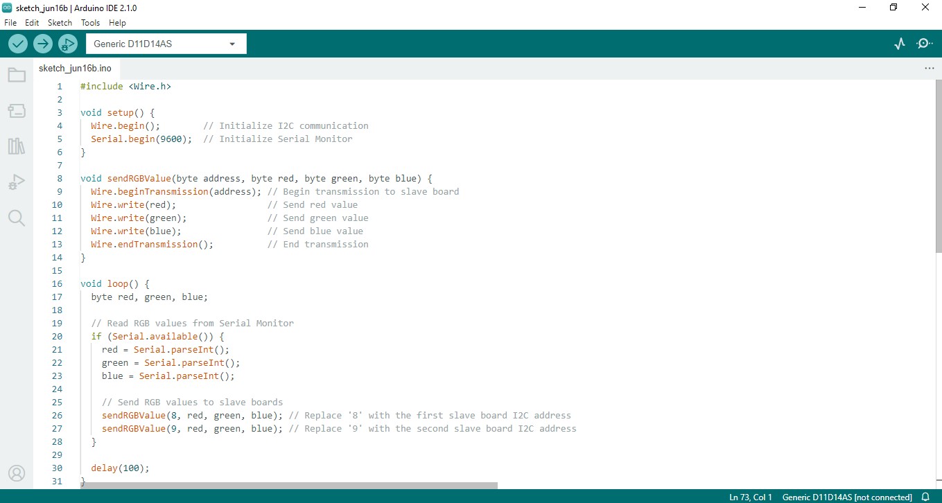
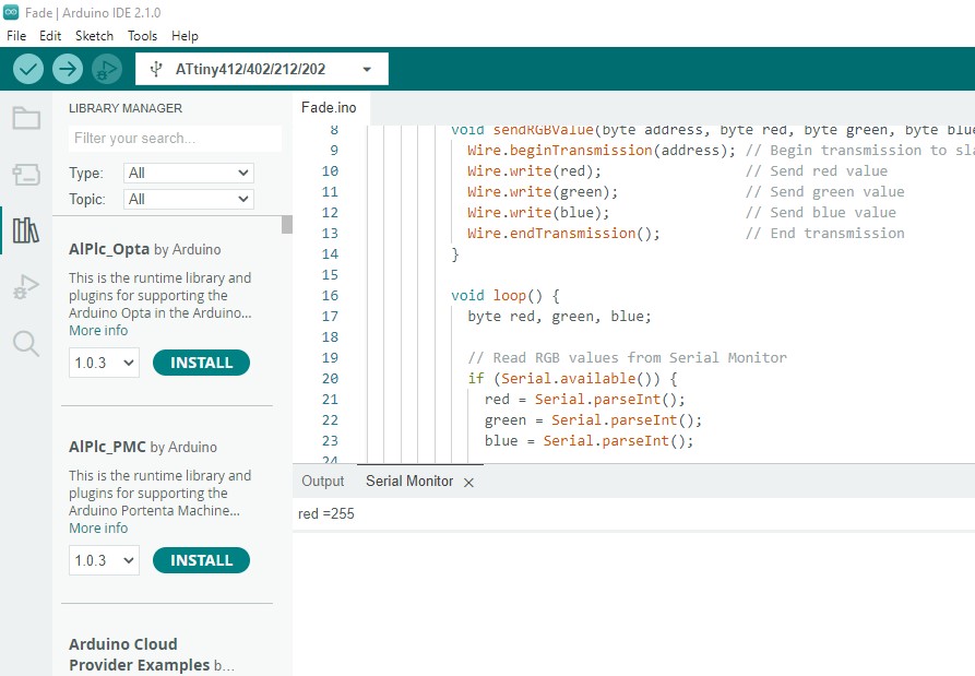
The provided code facilitates bi-directional communication between the user and the slave boards using I2C protocol. It allows the user to input RGB values through the Serial Monitor, which are then transmitted to the specified slave boards. The code reads the RGB values from the Serial Monitor and utilizes the sendRGBValue function to initiate I2C transmission to the slave boards, sending the red, green, and blue values. This enables simultaneous control of the RGB LEDs on each slave board based on the RGB values received. Overall, the code provides a streamlined method for controlling the RGB LEDs on the slave boards, enhancing the flexibility and synchronization of multi-board setups.
The computer is connected to the master using a serial monitor and is connected to the board. We can type in the color combination of the slave, which can be changed using the serial monitor. In the serial monitor, we can define the color of the LEDs by changing the PWM output of the program. To do that, we need to send the data in the form of signals. The LED is connected to the common ground. If the PWM output is 0 for red, blue, and green, it will give white. The ranges vary from 0 to 255 in reverse order of the primary colors.
The provided code serves as the foundation for establishing a robust communication channel between the master and slave boards, enabling the master to control the behavior of the RGB LED on the slave board. Through the utilization of the I2C communication protocol, the master board can seamlessly transmit RGB values to the slave board, dictating the desired color and brightness of the LED. This synchronization between the master and slave boards allows for precise control and coordination, unlocking a myriad of possibilities for interactive applications and creative LED-based systems. By leveraging the power of I2C communication, this code empowers the master board to efficiently command the slave board, resulting in synchronized and responsive LED control.
Overall, the week proved to be a productive one, enabling me to achieve my objectives of establishing wire-based communication and exploring the capabilities of I2C. The experience not only enhanced my programming skills but also deepened my understanding of the intricacies involved in microchip communication. The successful control of the LED's color using the serial monitor validated the efficiency of the implemented system. Encouraged by this accomplishment, I am now motivated to further explore and apply wire-based communication in my future projects.