
ELECTRONICS DESIGN
WEEK - 6
Objective
- Group assignment:(Page Link Here)
- Use the test equipment in your lab to observe the operation of a microcontroller circuit board
- Individual assignment:
- Design a development board to interact and communicate with an embedded micro-controller
CONTENTS :
As I come from a mechanical engineering background, I had limited exposure to electronics design But, I did have some familiarity with the basics, which made it easier for me to learn.
I did watch some YouTube videos and read some blogs about circuit design, to get a quick idea.
Tasks this week:
- Schematic design
- PCB design
Some of the basic and common electronic components,
- Resistors: resists the flow of current by dissipating electric power as heat.
- Capacitors: The function of capacitors is to temporarily hold electric charge, and release it whenever more power is needed elsewhere in the circuit
- Inductors: They store energy but instead of storing electrostatic energy, inductors store energy in the form of a magnetic field that generates when current flows through them
- Diodes: It is a device that allows current to flow in one direction only, from the anode (+) to the cathode (-).
- LED: is a diode that emits light when electricity passes through it.
- ICs: or integrated circuits are the circuits and components that have been shrunk down onto wafers of semiconductor material
- Transistors: a semiconductor device used to amplify or switch electrical signals and power
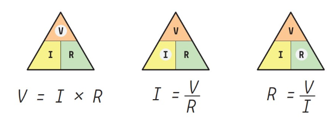
Ohms law
Ohms law: An increase in voltage through a circuit with a constant resistance results in an increase in current flow, and a decrease in voltage leads to a decrease in current flow.
This law is used extensively in electronics design to calculate the values of components such as resistors and to ensure that circuits are designed to operate within safe and desired voltage and current ranges. so it is worth noting.
V= I x R
this equation will be used in most cases for finding the value of the resistor
PCB designing
Electronic design software or EDA software
EDA software tools are used to create schematic diagrams, printed circuit board (PCB) layouts, and perform circuit simulations.
Some of the EDA software are:
- Fusion 360 Eagle Cad.
- KiCad
- OrCAD
- EasyEDA
- Altium designer
So here for PCB designing I used Fusion 360 ECAD, since most of the projects here were done in the Fusion 360, so it was easy to learn and adapt to it as a beginner, and it is also very convenient to do all the designing in a single software, and at the end of this assignment, I would also like to check out other software like KiCad.
Schematic design
It is a circuit diagram or the functional diagram of electronic circuits. Where symbols are used to represent components and show how they are connected electrically.
here's a detailed explanation of the schematic diagram
To create a schematic diagram in Fusion 360
- Open Fusion 360, go to File → New Electronics Design
this opens a new window
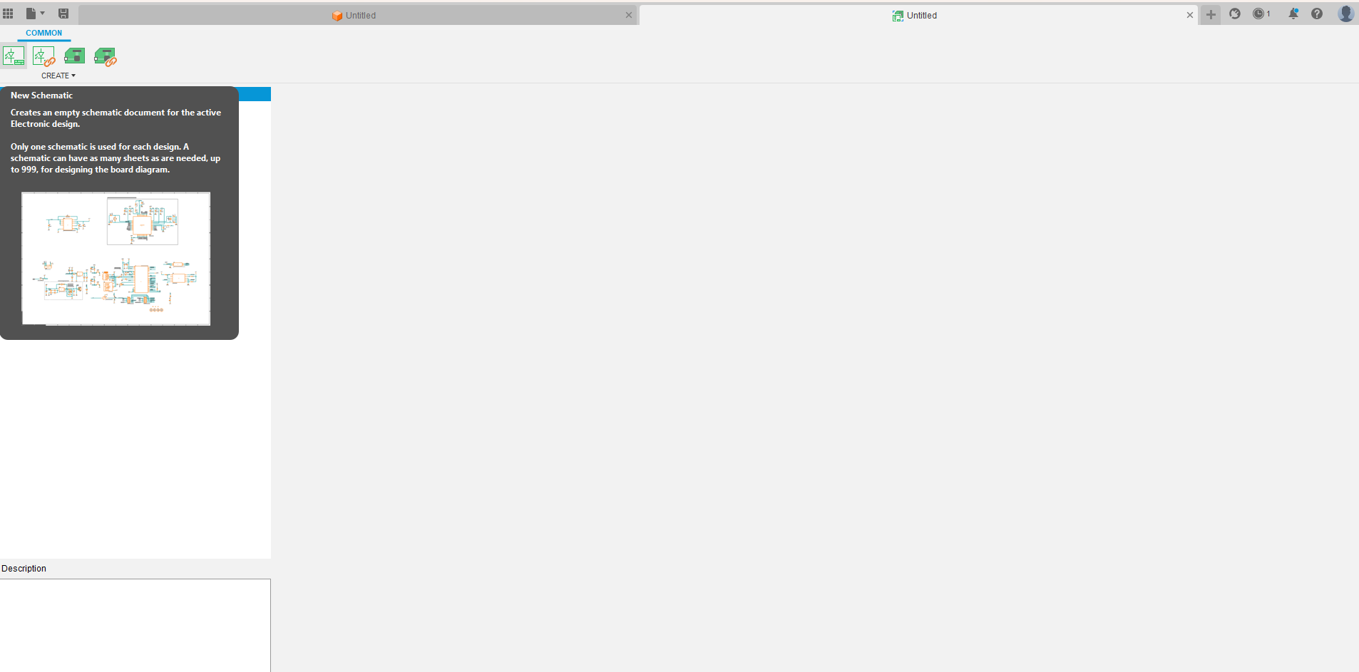
- Click on New Schematic Design, and now a new tab will open.
Adding the library
Our academy instructor Jojin shared a detailed library that almost had all the components of our inventory
To add the library, Go to Library Pane, and click on Open Library Manager.
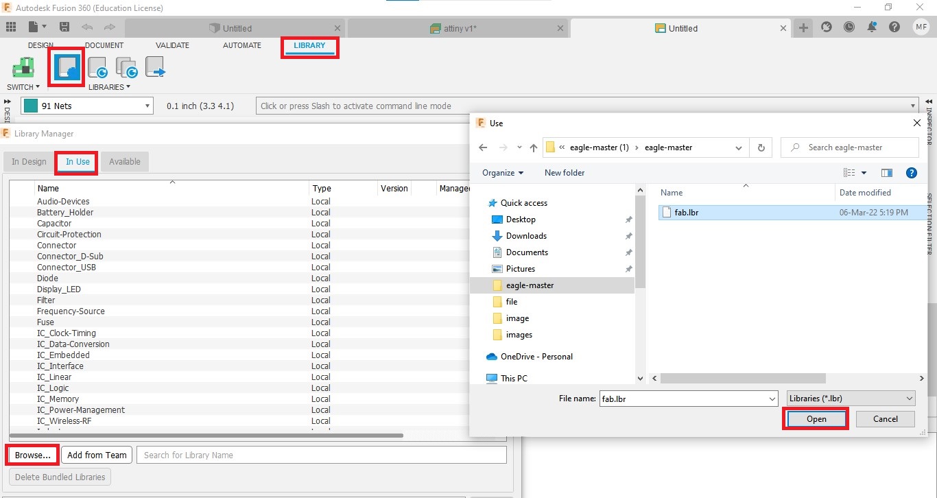
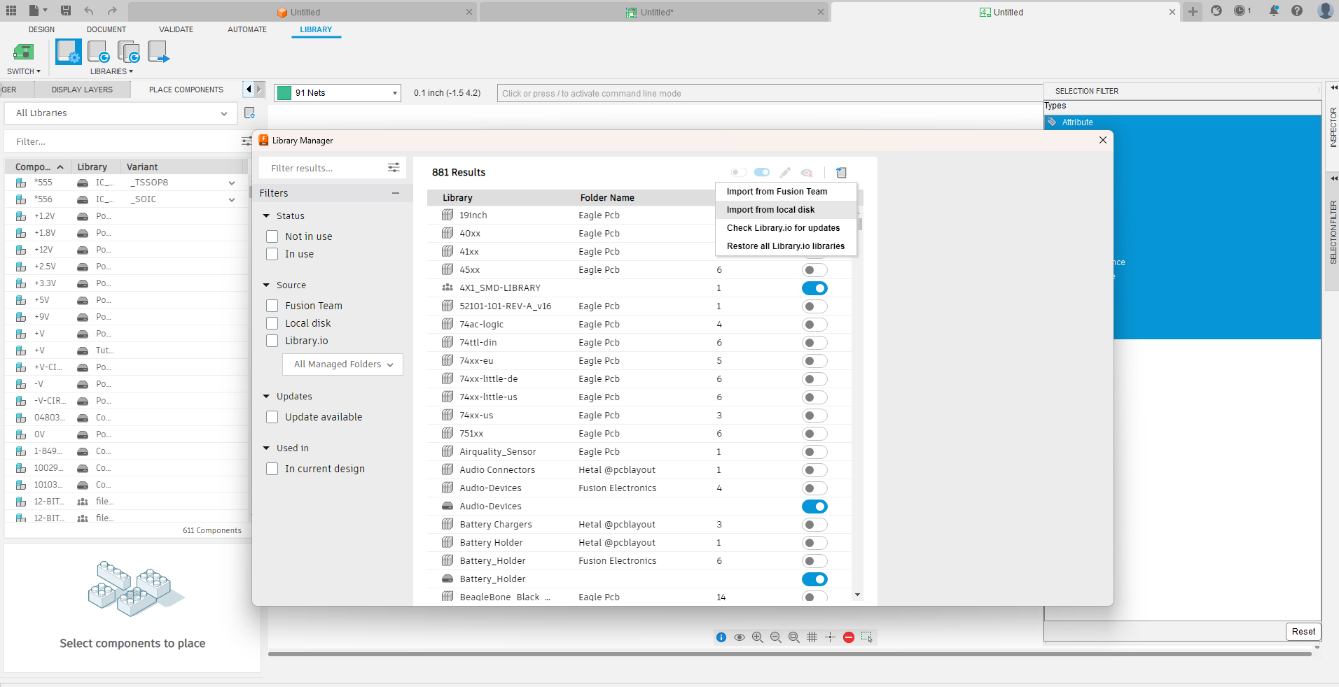
In the next window, go to In Use → Browse → select the file with .libr extension.
This week I will be using an ATTINY microcontroller, which was already added in the library,
but some components like a 6-pin head were not in the library so had to add it manually,
Creating, Editing a component
for adding a component
Go to File → New Electronics Library
In the opening tab, click on Create New Device icon and import an existing file.
I changed the names, added icons, and edited the pin and pad connections.
- this is the pin head I made a 1x4 SMD female pin,
- added the footprint according to the one available in our inventory
- and also replicated this for a 1x4 SMD male
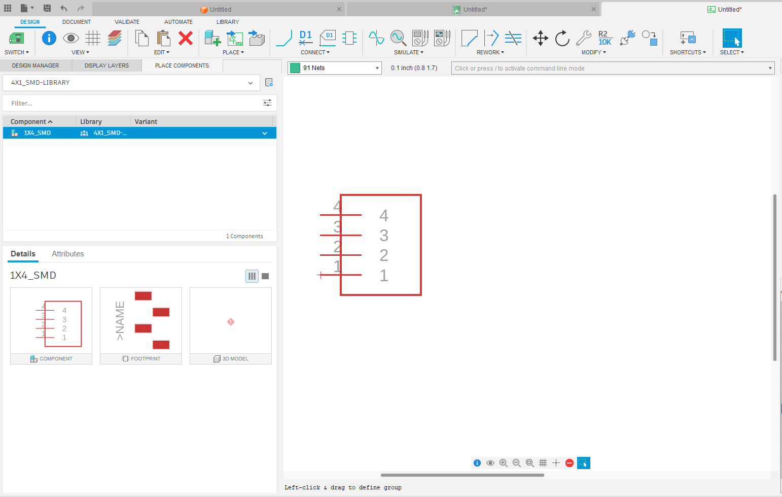
After saving the file, I added the device to the library.
Create a schematic diagram
Go to the Design Pane and click on Add part icon, and I added different parts for the circuit.
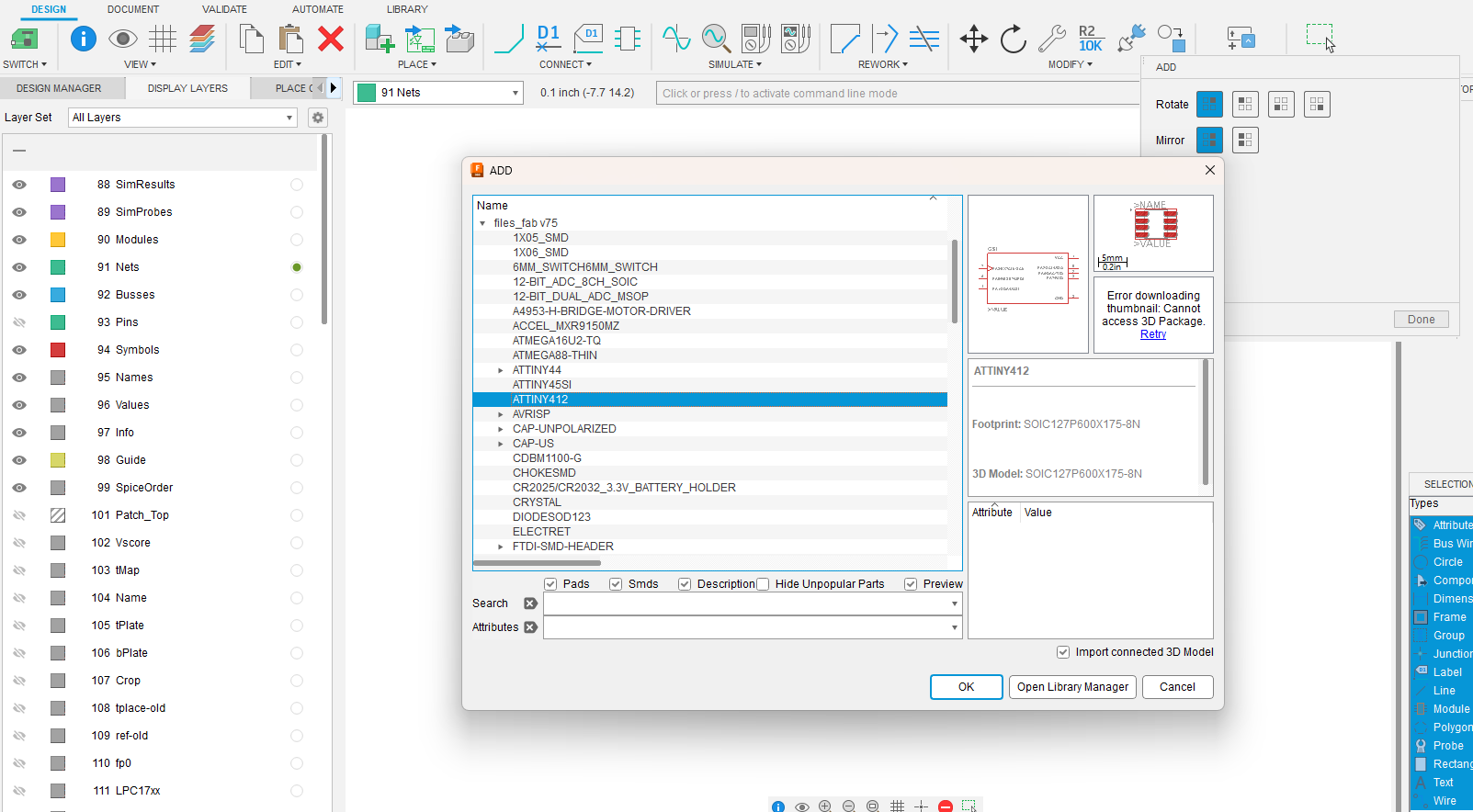
Parts I added:
- ATtiny 412 = 1
- Resistor = 2
- Capacitor = 1
- LED = 1
- switch = 1
- (CONN_06_FTDI-SMD-HEADER) = 1
- PDI_2X3_SMD_UPDI = 1
Using the move and rotate options, we can position various components.
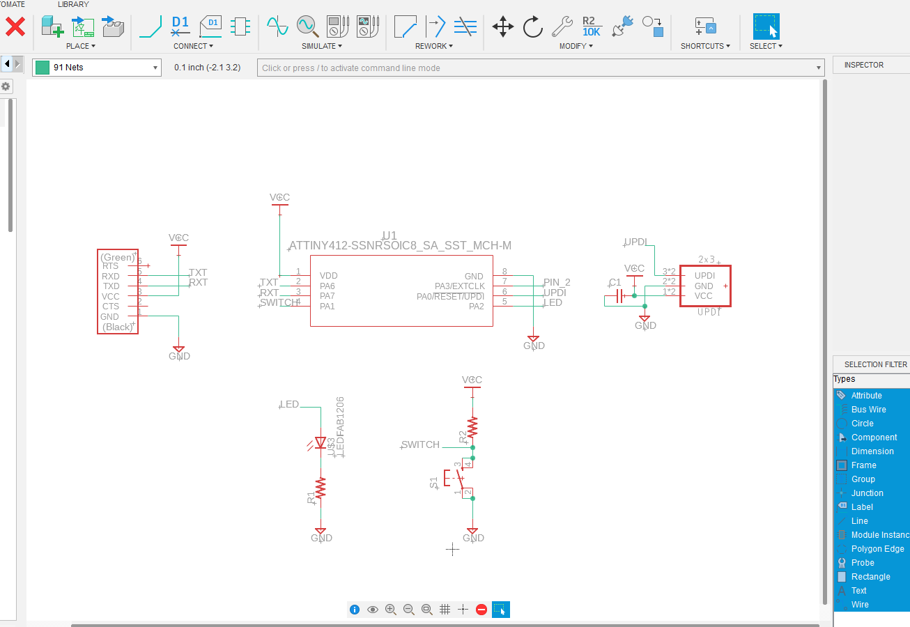
we can use nets to link components with the reference image.

for adding the LED and switch
- To add an LED to the circuit, I connected one leg of the LED to a resistor and then to the ground, and the other leg to a pin on the microcontroller. For the switch, I connected one leg to the ground and the other to a pin on the microcontroller.
Adding the Ground and VCC.
Instead of complex wiring connections, We can use schematic parts like ground and VCC. For some connections, I used the Label tool.
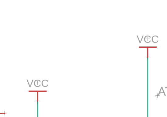
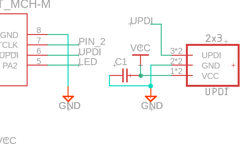
- Instead of manually routing wires across components, we can utilize VCC (power) and GND (ground) symbols to connect power and ground. It is considered a good practice to give directions to "up" for all VCCs and "down" for all grounds.
In a schematic diagram, we can use symbols instead of drawing wire connections. Symbols with the same net names will automatically be connected.
- After completing the schematic diagram, click on Switch to PCB document icon (green icon in the top left corner)
- In the new tab, adjust the canvas size an arrange the components for connecting
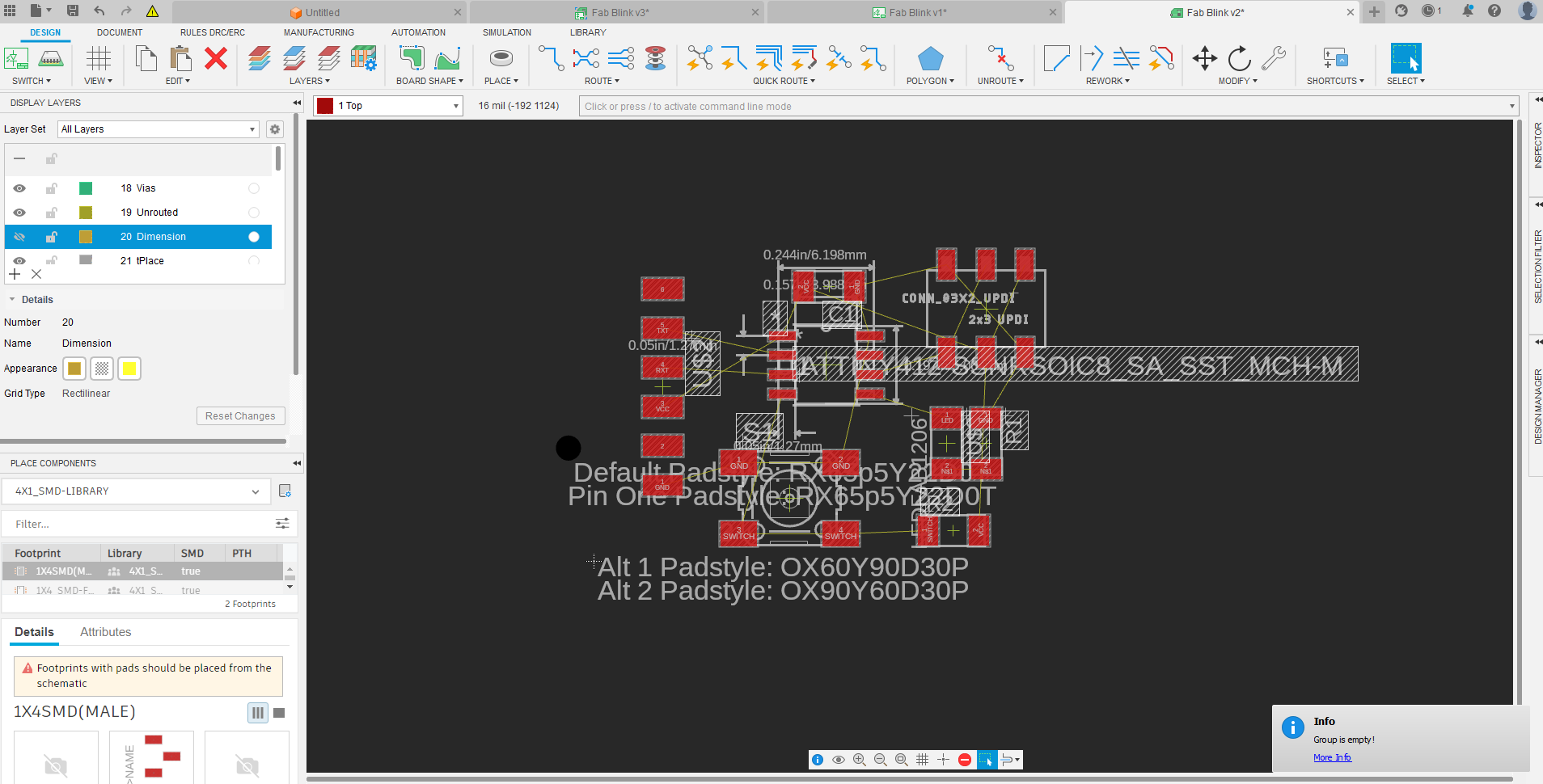
- We can arrange each component by using the move tool and rotate tool.
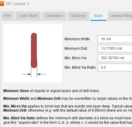
DRC- Design rules
- after that Go to the RULES ERC/DRC. and click on the DRC icon.
In the opening window, we can set design rules for PCB milling.
- here we use 16 mils bit and 32 mils bit. I set values like clearance, hole width etc, this will be cleared and tested in the electronics production week
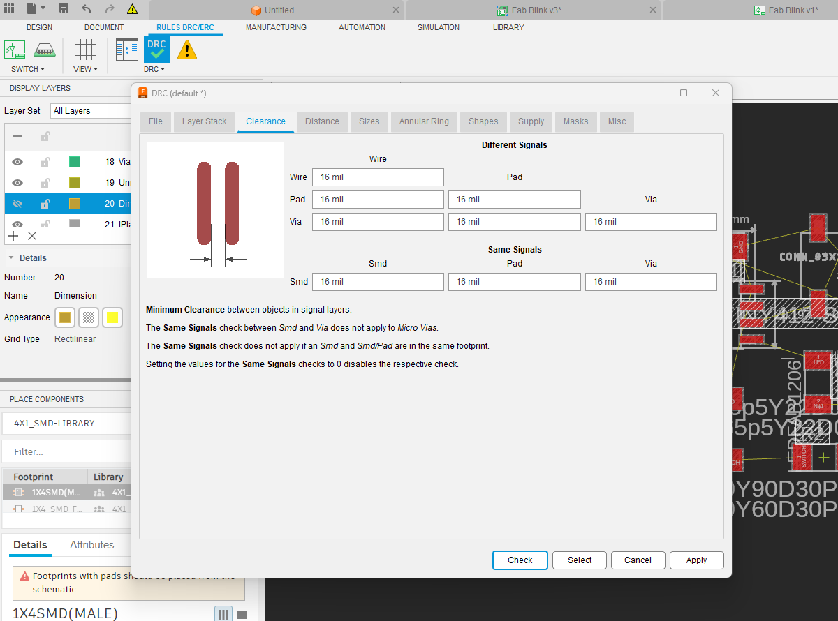
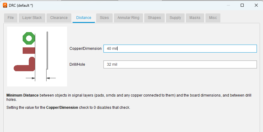
- After setting design rules, click on apply.
- NowReturn to Design Pane. and go to Quick Rout e→ Auto-route.
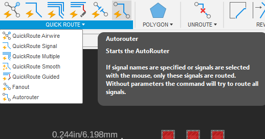
- In the opening dialogue box, select N/A for all layers except Top. Because we are designing a PCB for solder SMD components, and it is a single layer PCB, also it can be routed completely and no number wires needed to be used
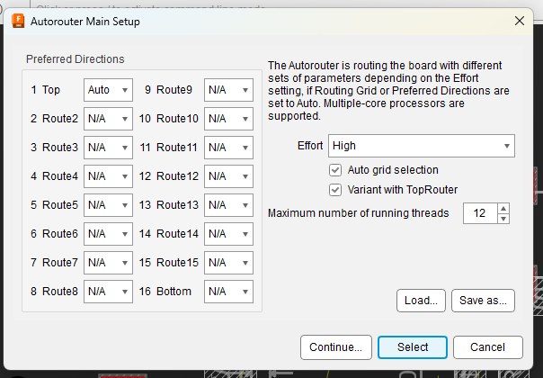
I selected Effort→ High and click on continue.
- In the opening dialogue box, click on Start.
- Initially, I was not able to get 100% connectivity in my circuit design due to some paths lacking proper routing.
- So to fix this, I used the "Ripup all" function to remove some of the complicated connections and rearranged the components.

- I kept trying different component arrangements and repeated the process multiple times. After each attempt, I checked the routing and made manual adjustments as needed. Finally, I achieved the desired outcome with the best trace arrangement.
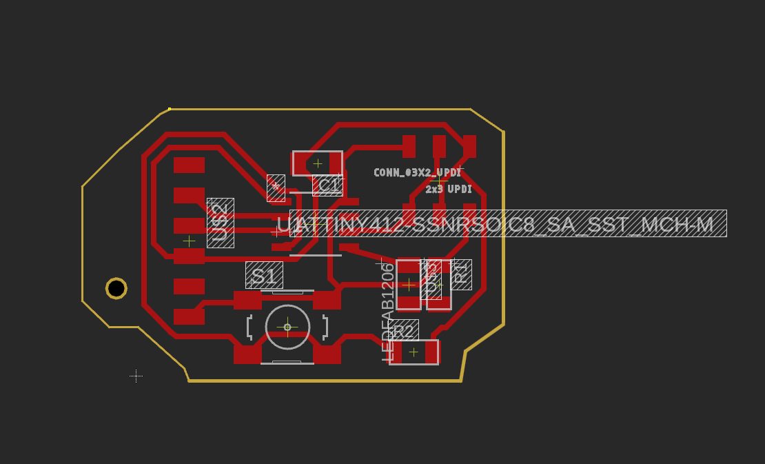
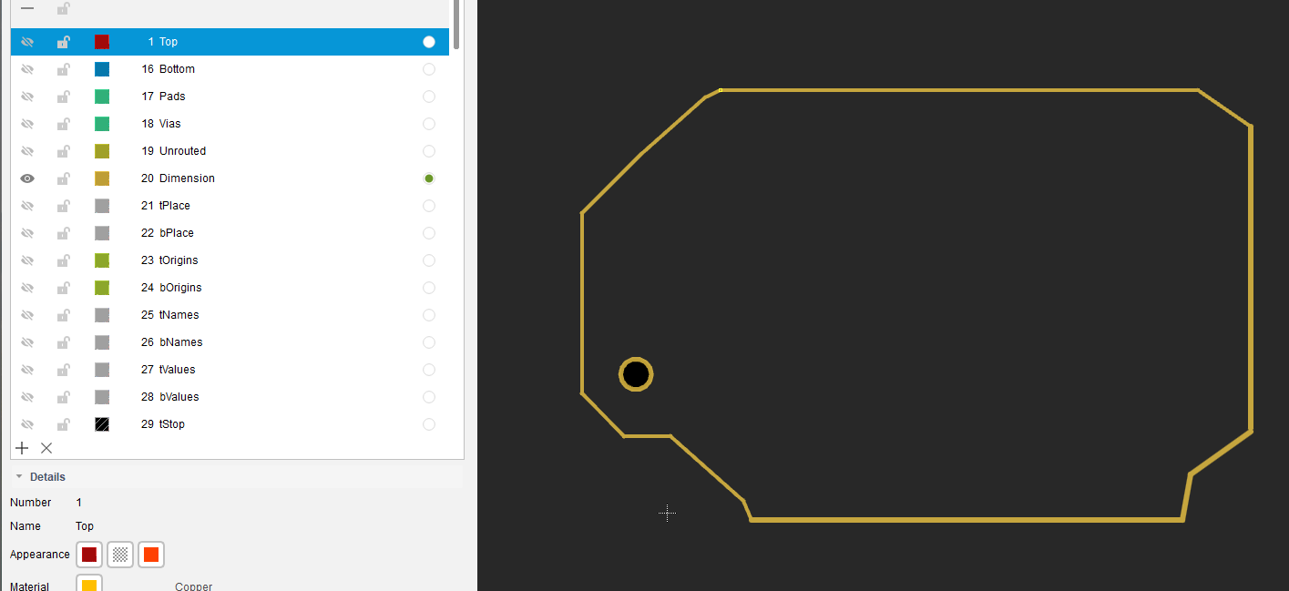
- also added an outer border for cutting out the PCB from a big sheet
- The next step is making export the milling path and cut the path for PCB milling.
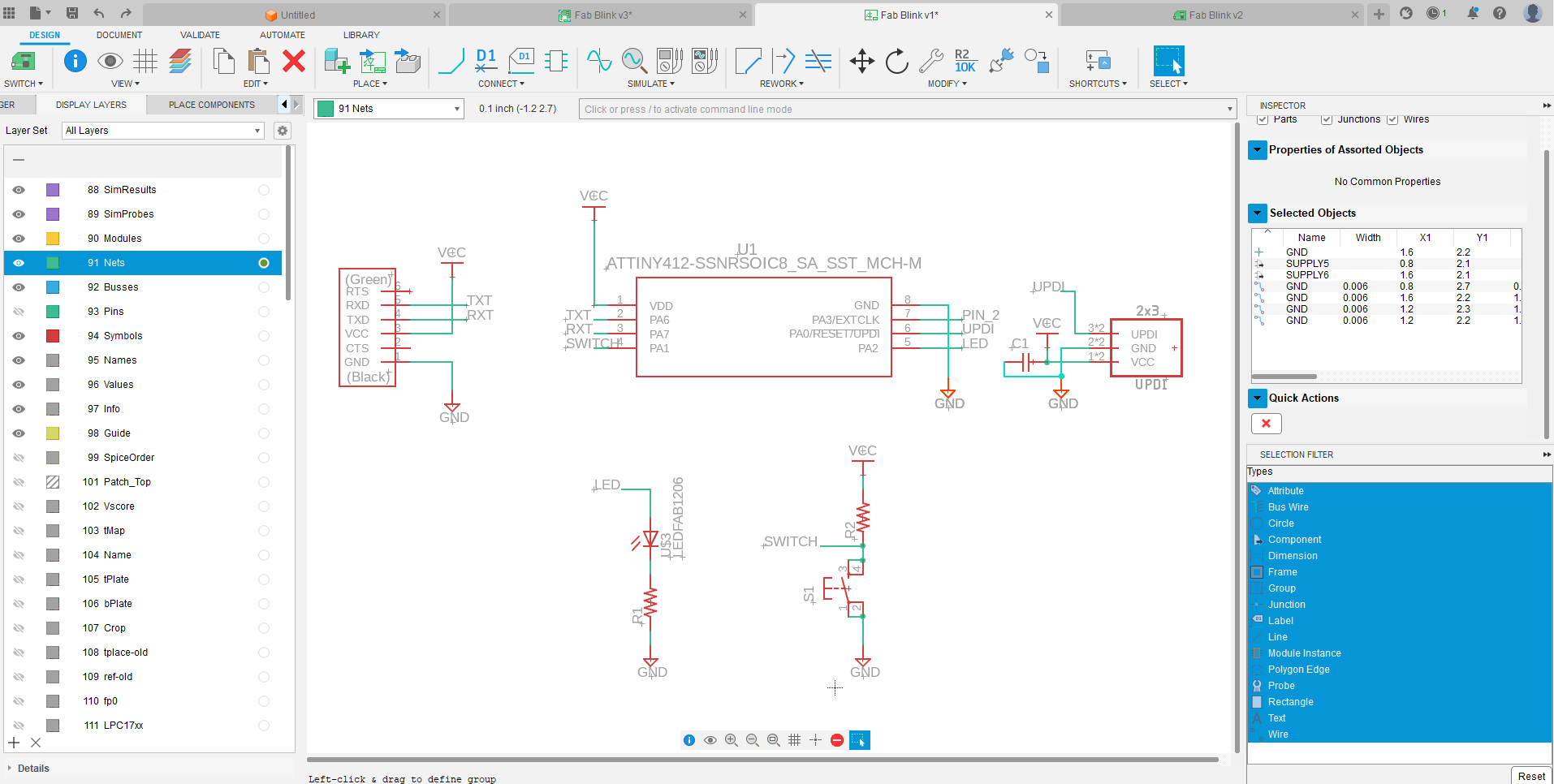
We can hide different layers of the design(route, name, etc.) by go to Layers → Display
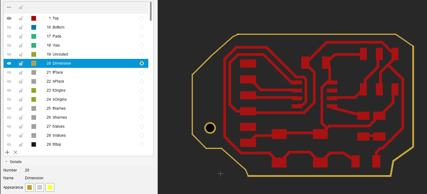
Export milling trace
Hide all layers except the top layer. Type export in the command box and press enter.
In the opening options select an image.
In the opening box.
- Specify a location >Tick on monochrome> Set resolution 1000.
and then click OK.
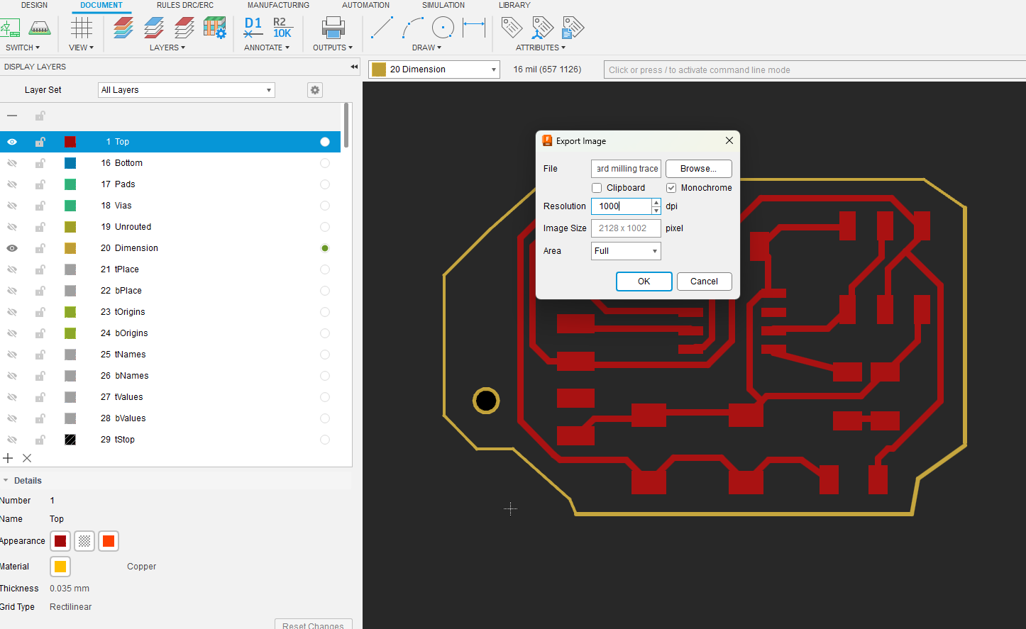
- the image will now be exported as .png file
- repeat the same for the outer cut and save it
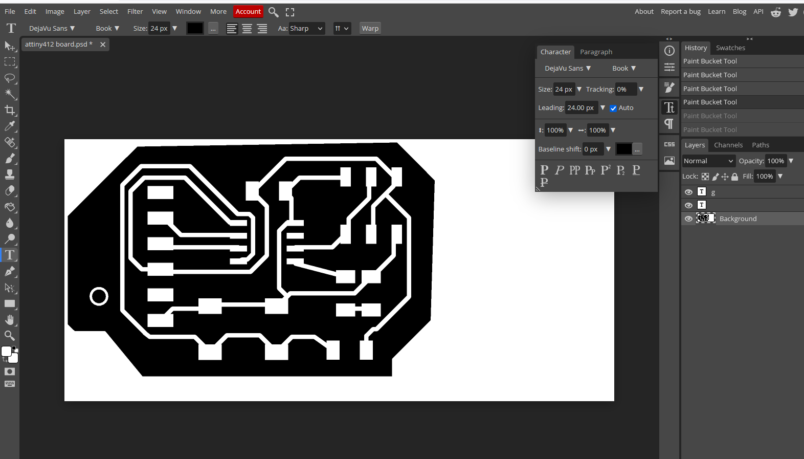
Editing the exported file
- I used Photopea to edit the image for better milling, adding labels
Design files
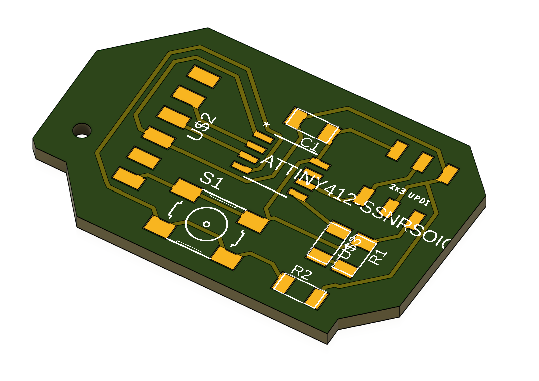
Schematic of the PCB:
Fusion 360 file of the PCB:
Traces for milling: