Week 6: Electronics Design
Tasks for this week
Group assignment
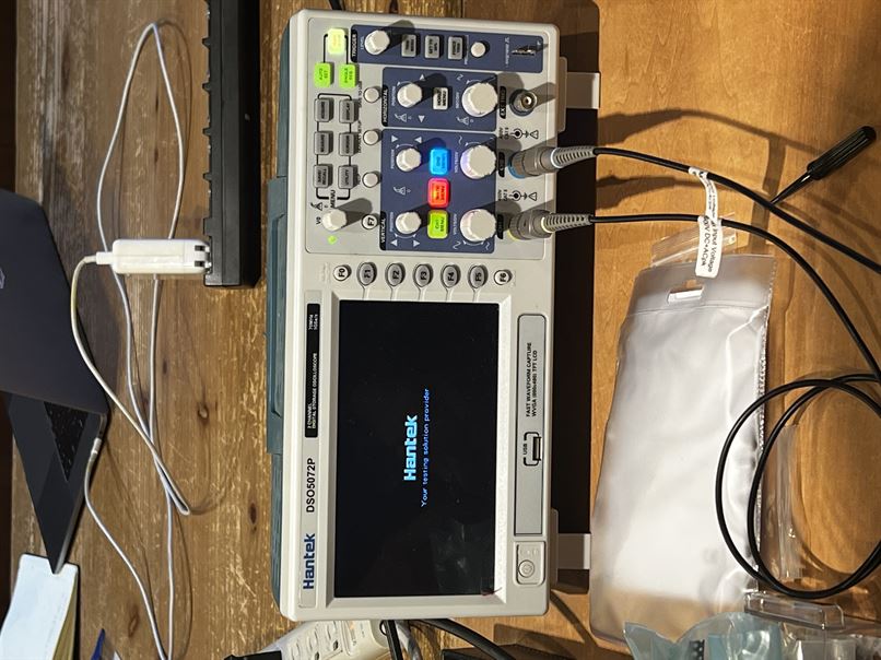
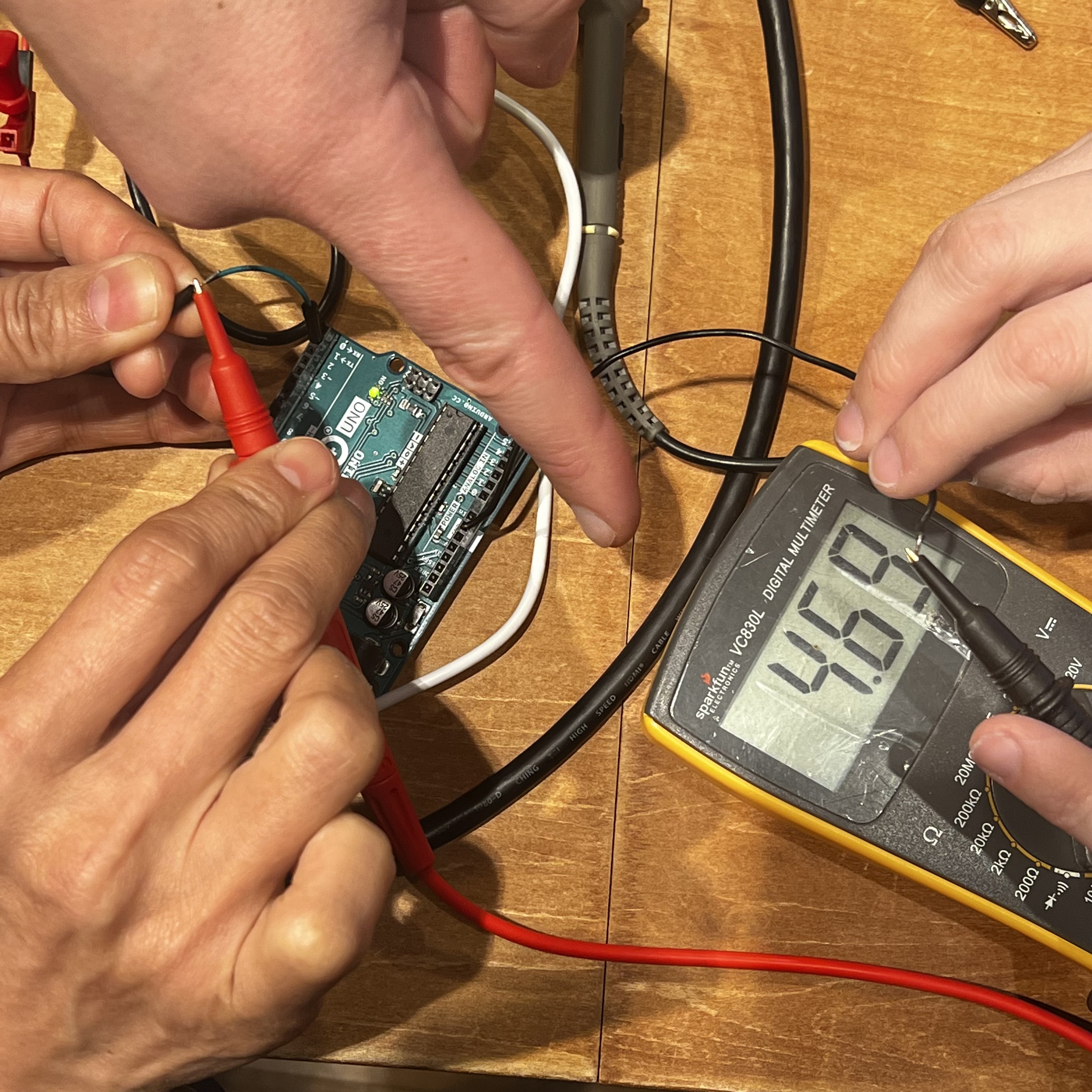
- Use the test equipment in your lab to observe the operation of a microcontroller circuit board (as a minimum, you should demonstrate the use of a multimeter and oscilloscope)
- Document your work on the group work page and reflect what you learned on your individual page
Individual assignment
- Design a development board to interact and communicate with an embedded microcontroller
Group Assignment
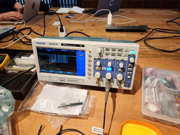
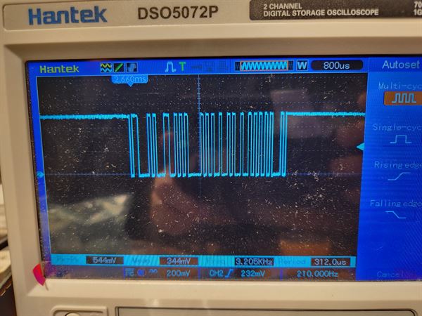
We were able to observe the output of an Arduino Uno board using an oscilloscope and a multimeter.
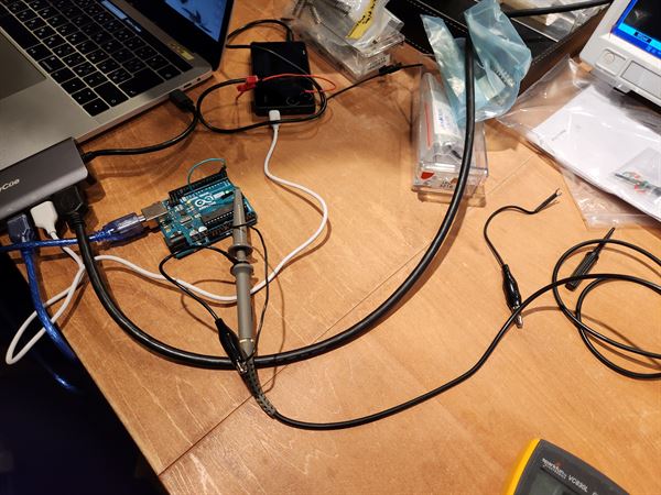
The most interesting thing for me was being able to observe the serial signal of my name visually using the oscilloscope

PCB Design using KiCad
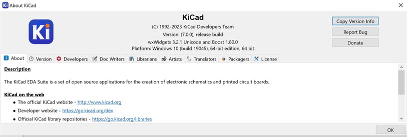
KiCad is a free software for designing printed circuit boards, the version used for this week's assignment is version 7.0.
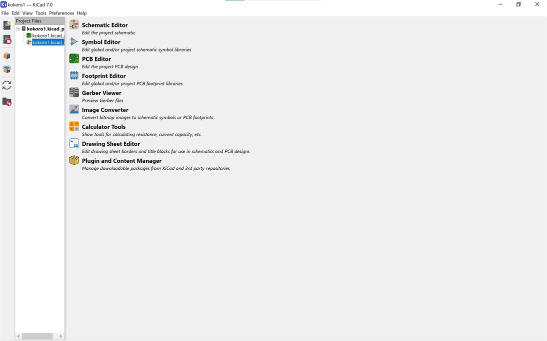
Setting up KiCad
Create a new project file and open Schematic Editor.
User Defined Libraries
users library info add
Creating the Schematic
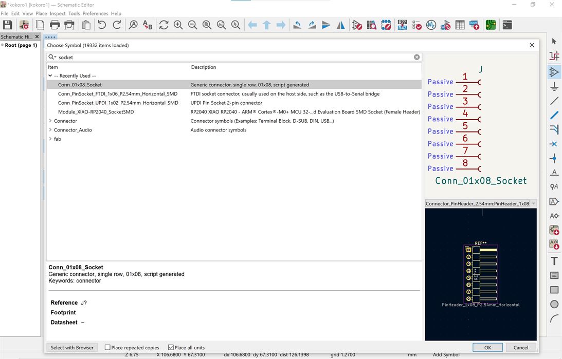
Add symbols to the Schematic by pressing 'A' on the keyboard.
You can then view and select the symbol you want to add.
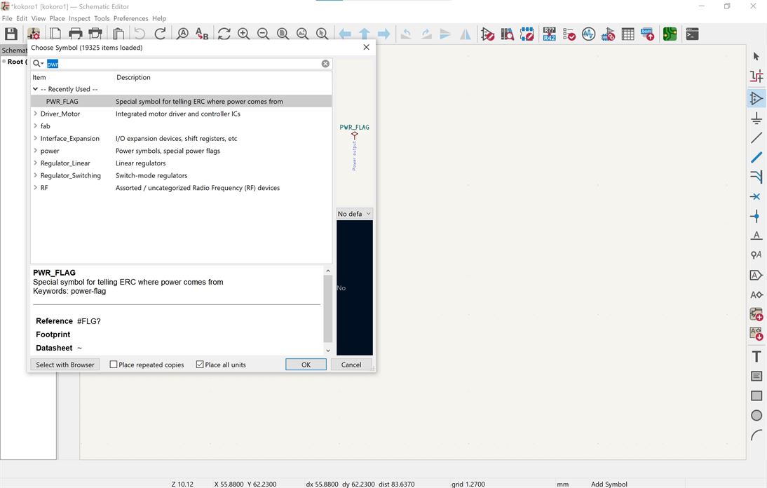
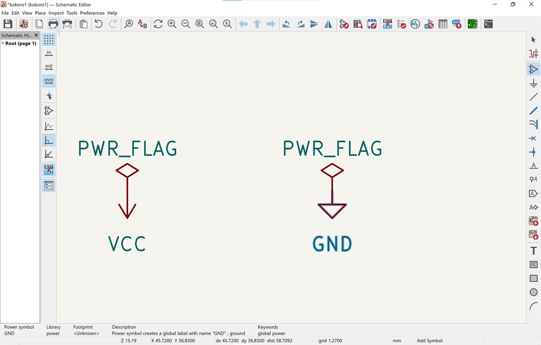
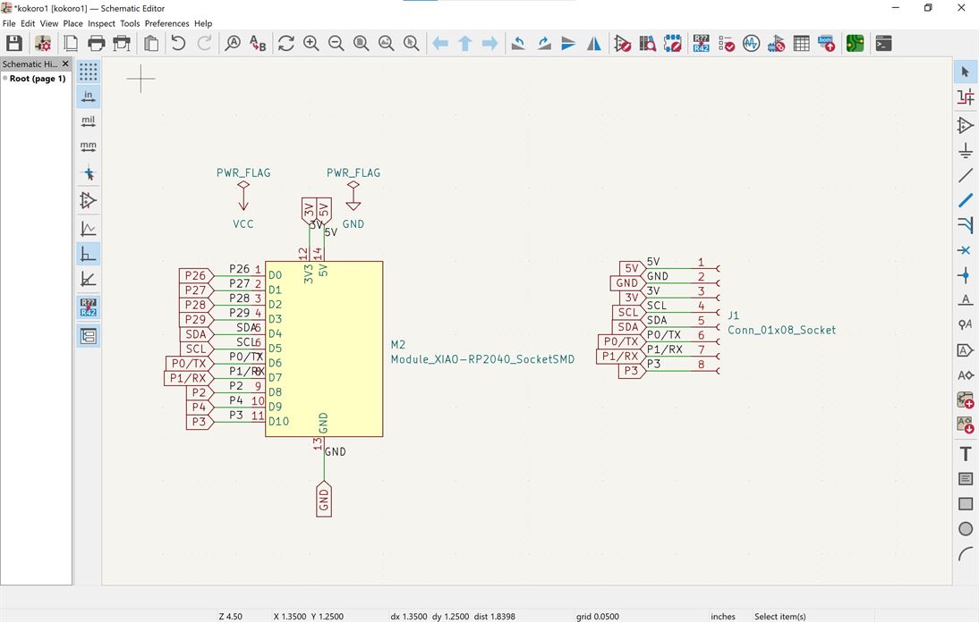
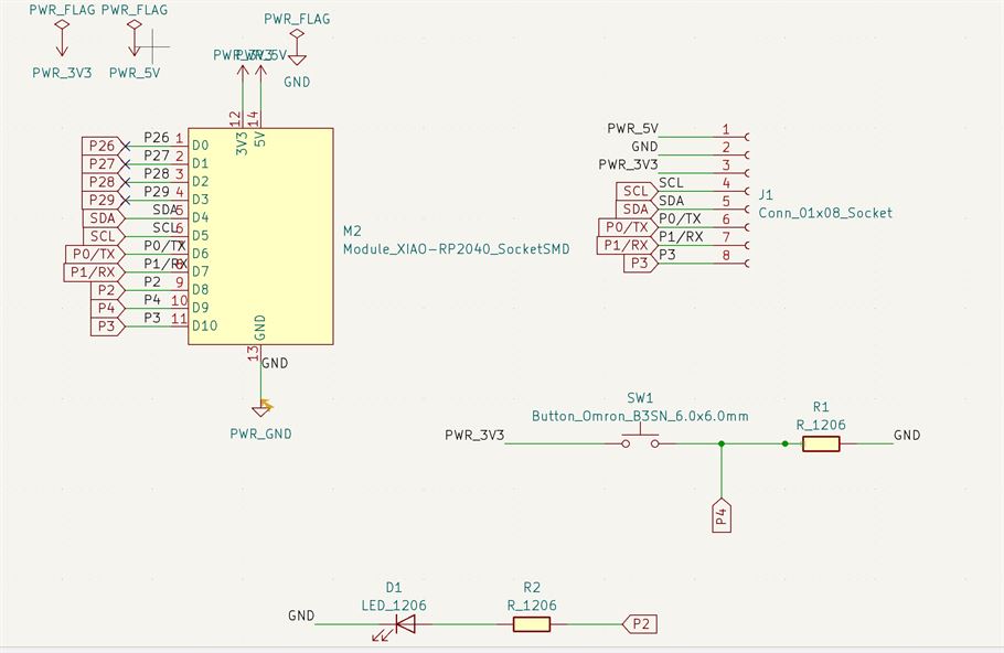
I started by adding power flags, to indicate items with power output and ground.
Symbols can selected and be moved to attach to each other.
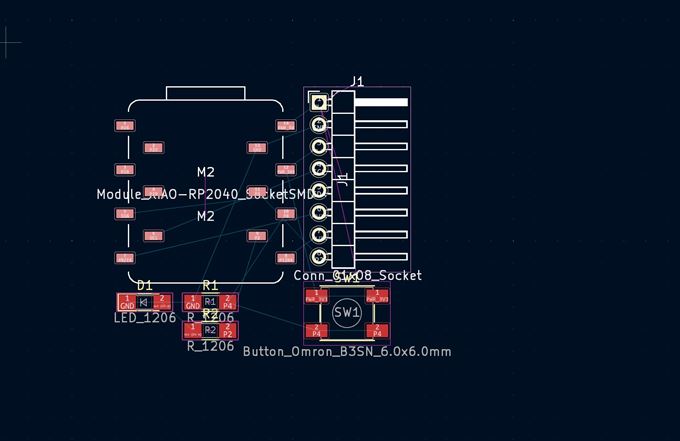
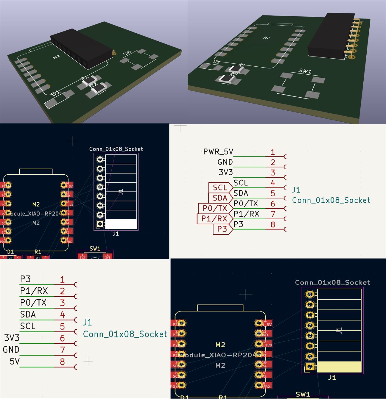
I then added the Xiao RP2040 and used the Wire option on the right hand side menu to add wires to the board. I then labeled the wires by selecting them and clicking 'L' on the keyboard.
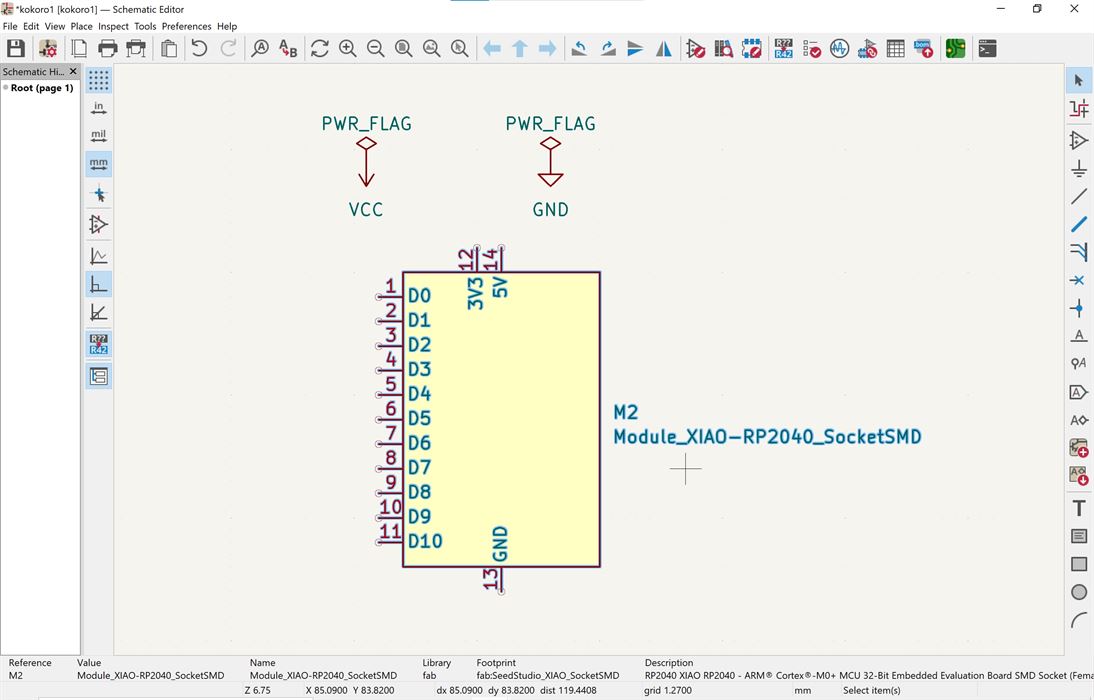
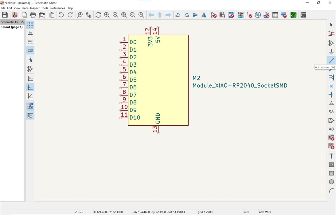
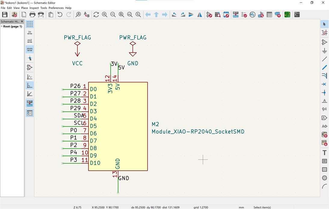
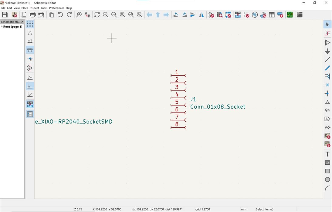
I then added a socket, added wires to it and assigned labels to match the Xiao.
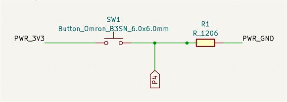
I added a button with 3.3V on one side (this will be able to be read as a signal when connected to a pin and feed into programming) and a connection to a pin, a resistor and ground on the other side.
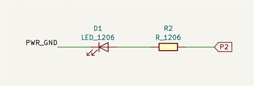
I added an LED (2 pin) with 5V and a resistor on one side and a pin connection on the other side so that I can program when the LED turns on/off.
I then selected used the electrical rules checker (checkbox button, top menu, 8th from the right) tool to check my design.
I got some errors due to the power flags. This was partly due to labeling not matching and symbols attached to the power flags and board not matching.
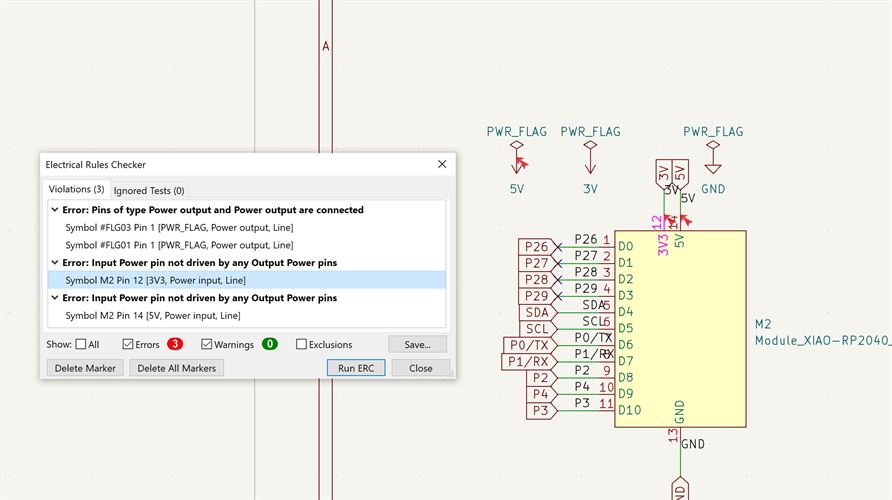
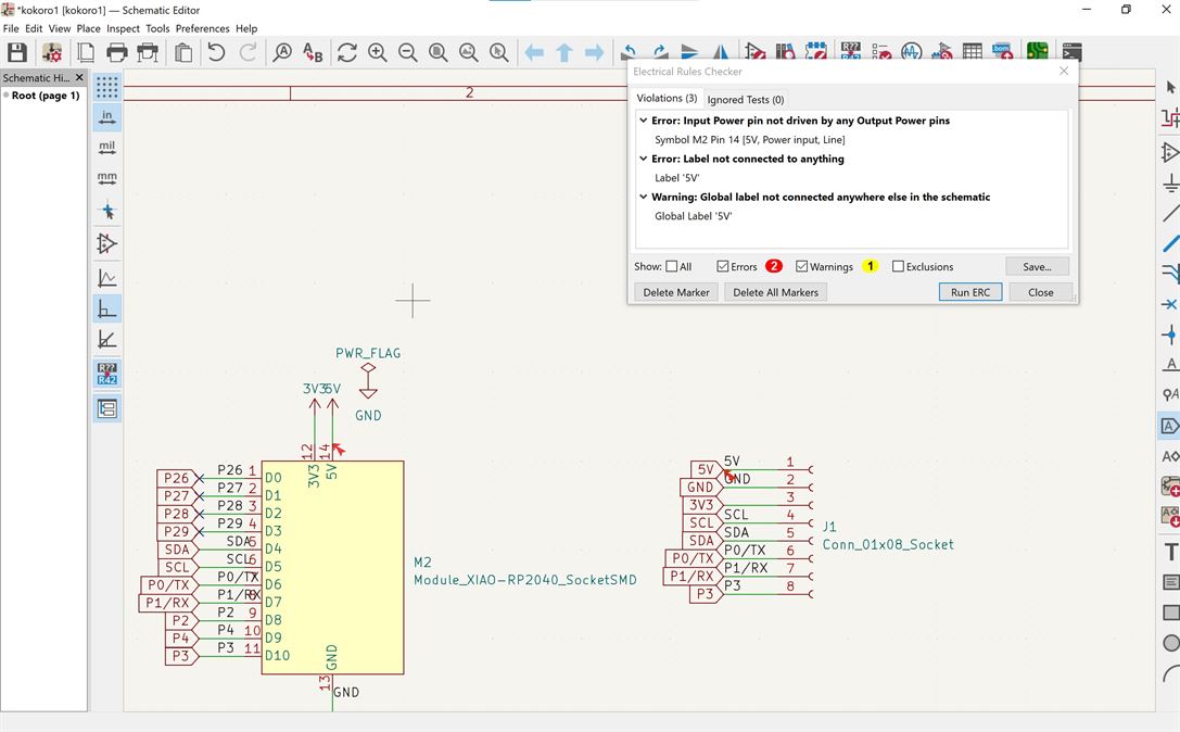
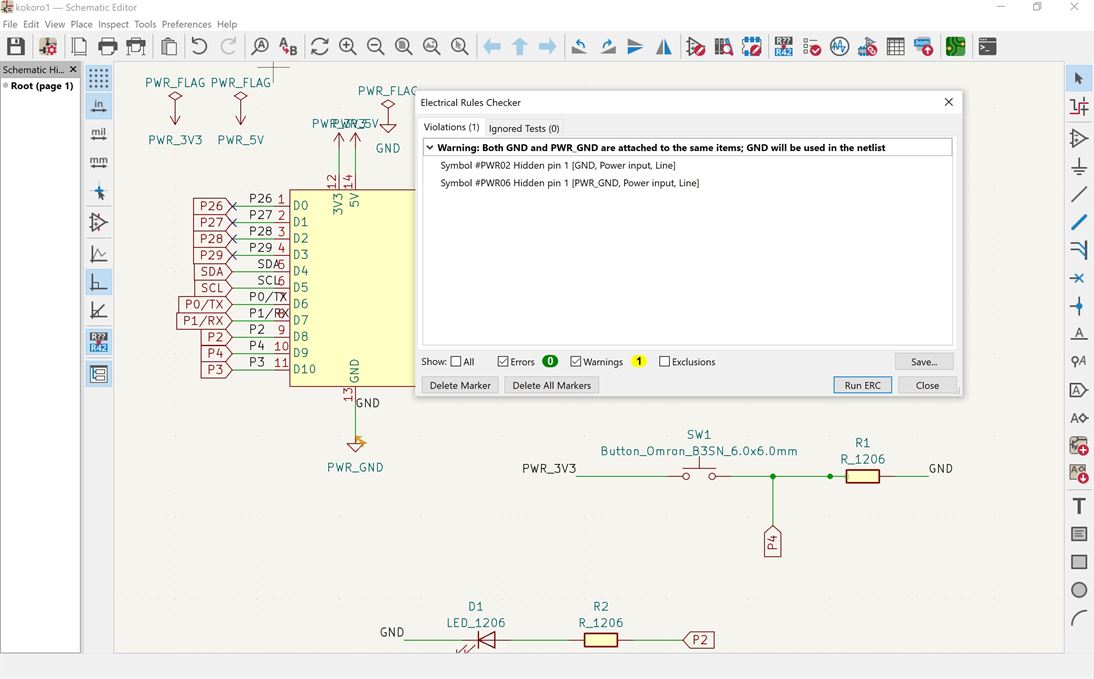
I corrected this and then got no errors or warnings.
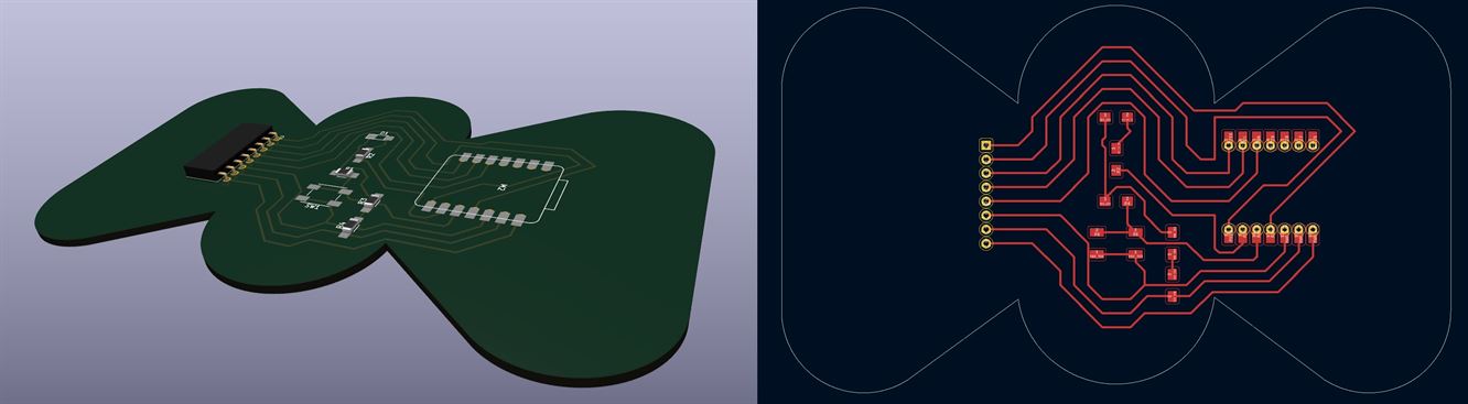
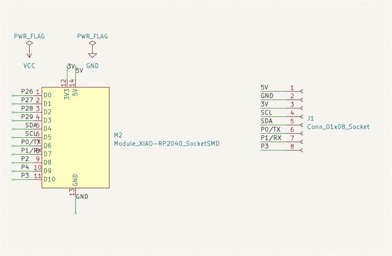
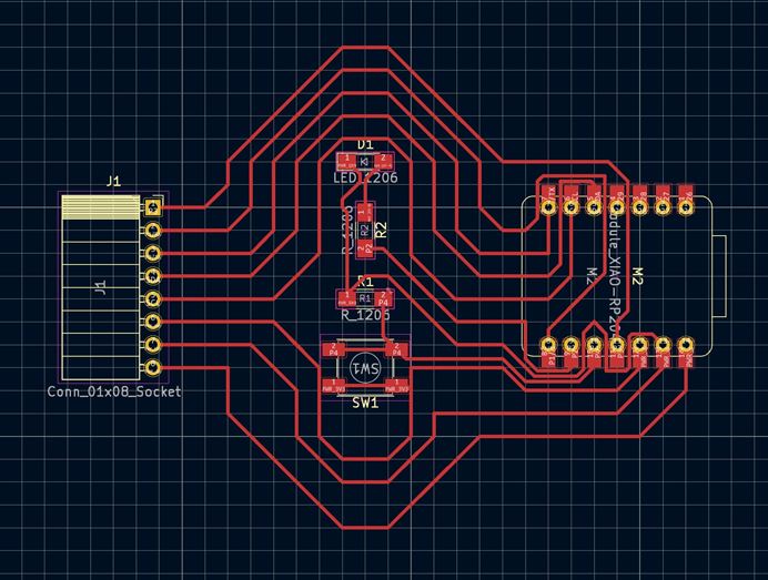
Resulting schematic
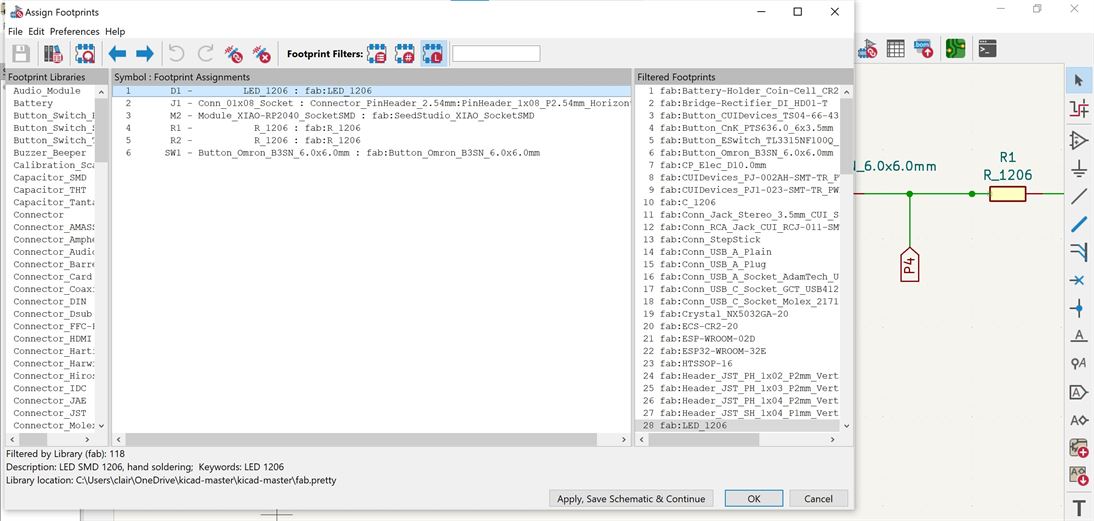
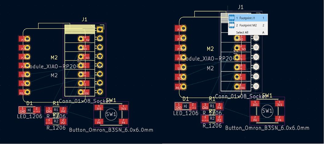
I used the assign footprints tool to check the assigned footprints for the schematic. (Button with link symbol on it, top menu, 5th from the right)
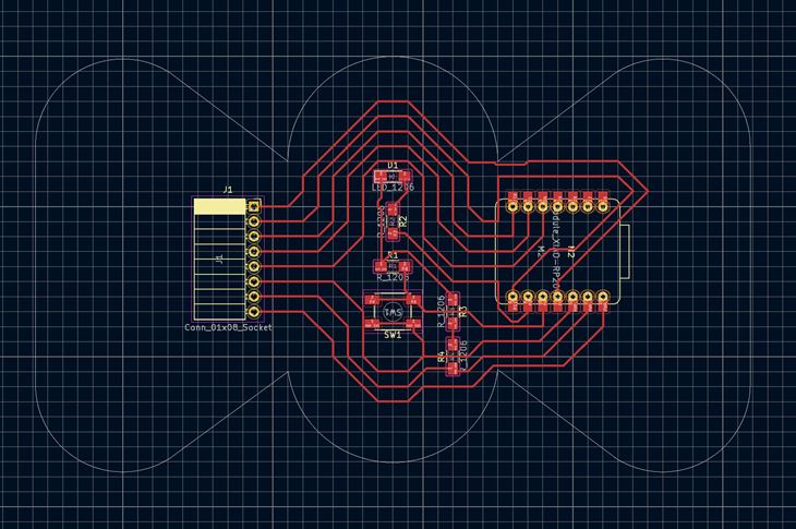
Board Design
I opened the schematic in the board editor.
I noticed that the layout for the Xiao was not the right one for what I wanted. So I went back into the schematic editor and changed the footprint used using the footprint assignment tool.
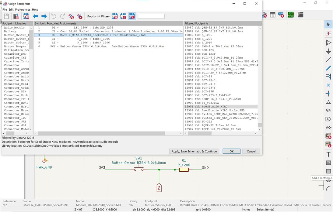
I looked at the design in 3D view and realised I had the wrong header - male header instead of female socket. I went back into the schematic editor and modified it using the footprint assignment tool.
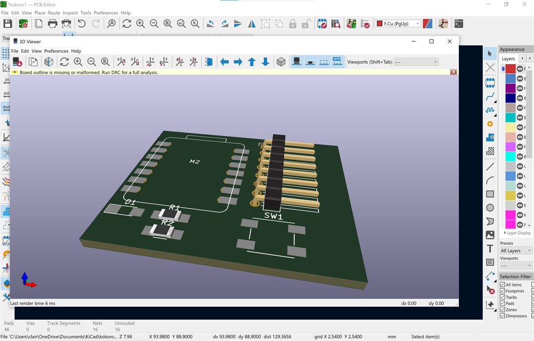
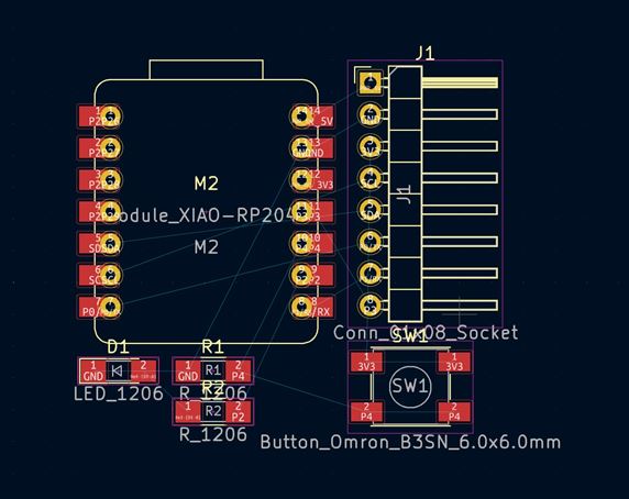
I then need to correctly move and orientate the socket so that it faces outward on the board.
This also involved editing labeling in the schematic to change the order of the connections to reduce the amount of crossover of the tracks on the board.
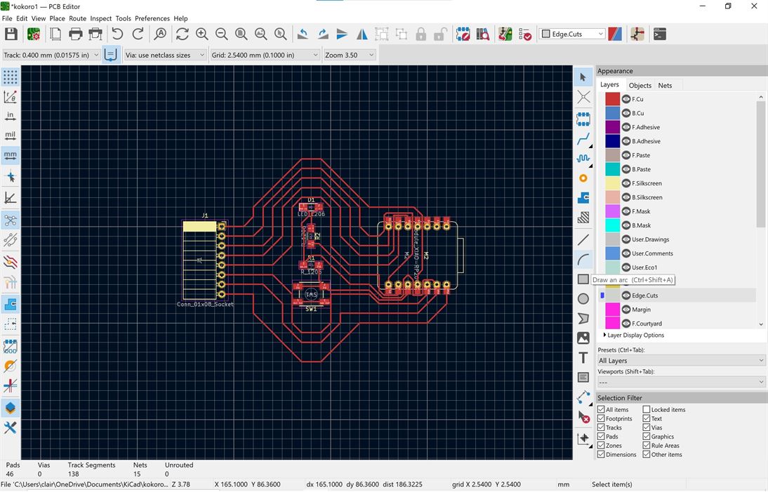
I then used the route tracks tool (right side menu) to create the traces. I made the tracks 0.4mm in size by setting a pre-defined track size.
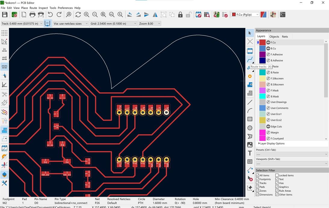
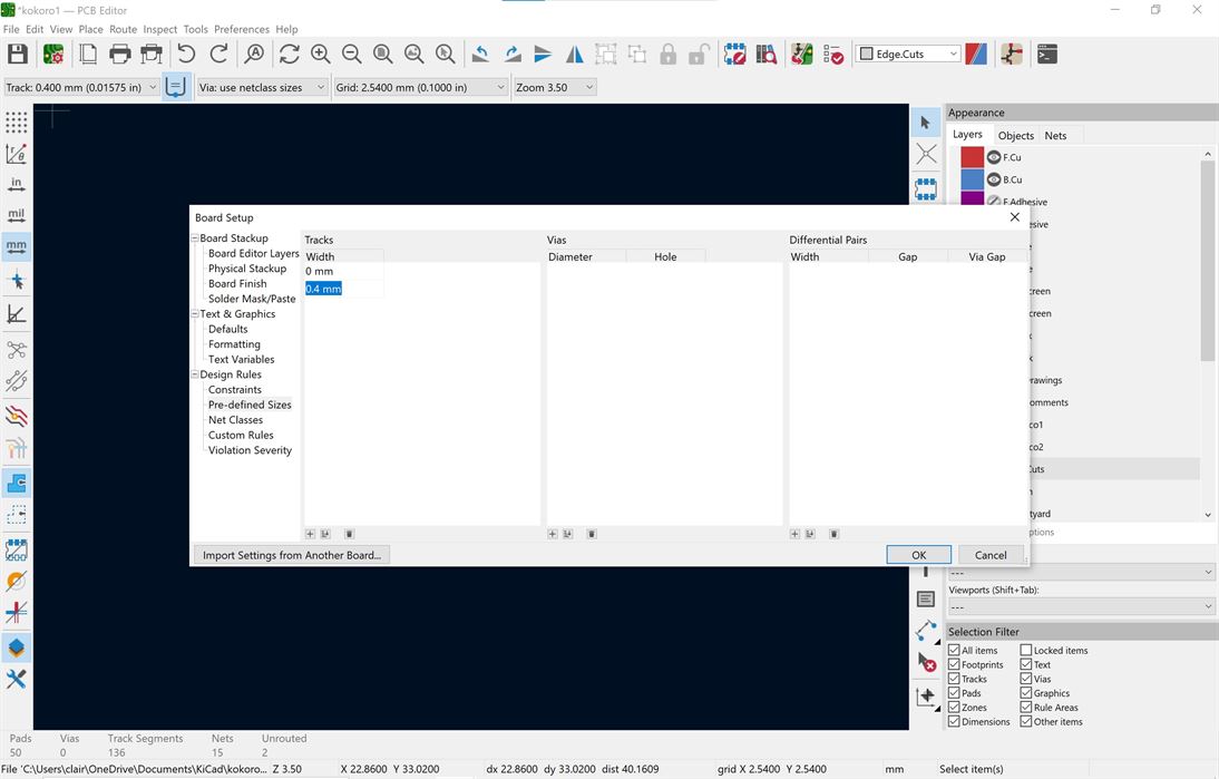
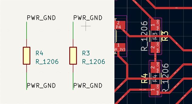
I realised that I had an issue with ground not being connected, so I decided to add zero resistors so I could bridge over other tracks. I also realised that some of my tracks were too close together, so I fixed them and also set a design rule to make sure they were a minimum of 0.4mm apart.
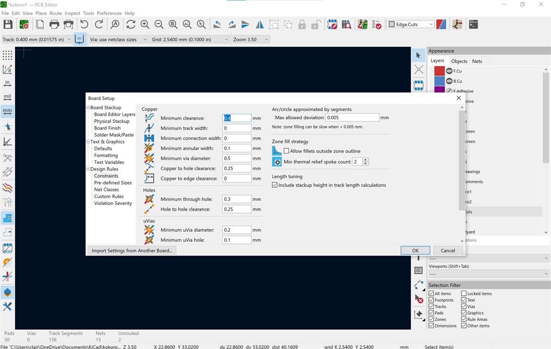
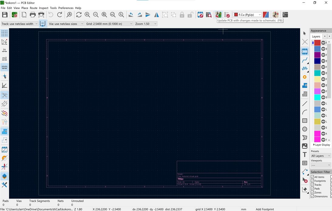
I then created the edge using lines to make the outside of the board.
I then ran the design rules checker and got back an error around the connection for the ground track going through the zero resistor bridges.
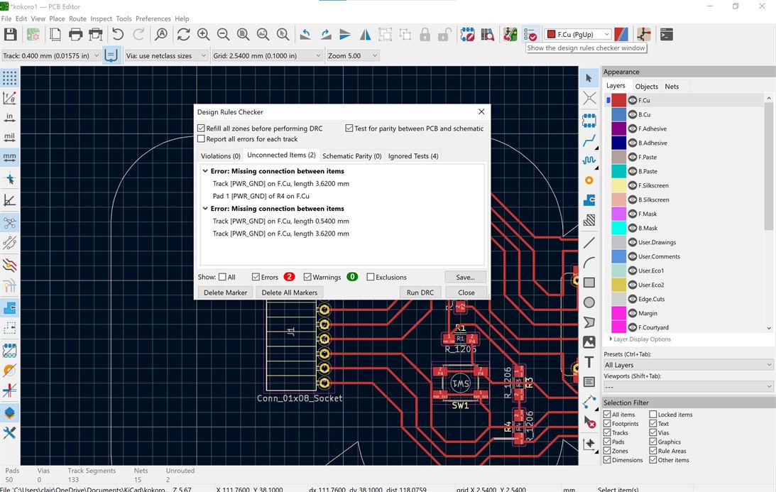
After doing some Google-ing I found that it looks like this error is because KiCad does not understand the bridging and that the board is fine for going ahead to production.
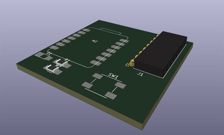
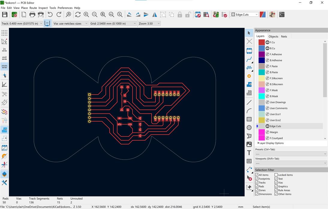
Final board