Electronics Design
Assignment
- Group Assignment:
- Use the test equipment in your lab to observe the operation of a microcontroller circuit board.
- Document your work on the group work page and reflect what you learned on your individual page.
- Individual Assignment:
- Design a development board to interact and communicate with an embedded microcontroller.
Evaluation Standards
- Linked to the group assignment page.
- Documented what you have learned in electronics design.
- Explained problems and how you fixed them.
- Included original design files (Eagle, KiCad, etc.)
- Included a 'hero shot'
Output Preview
Group Assignment
This week we want learnd about more about electronics, and It's designing & testing tools.
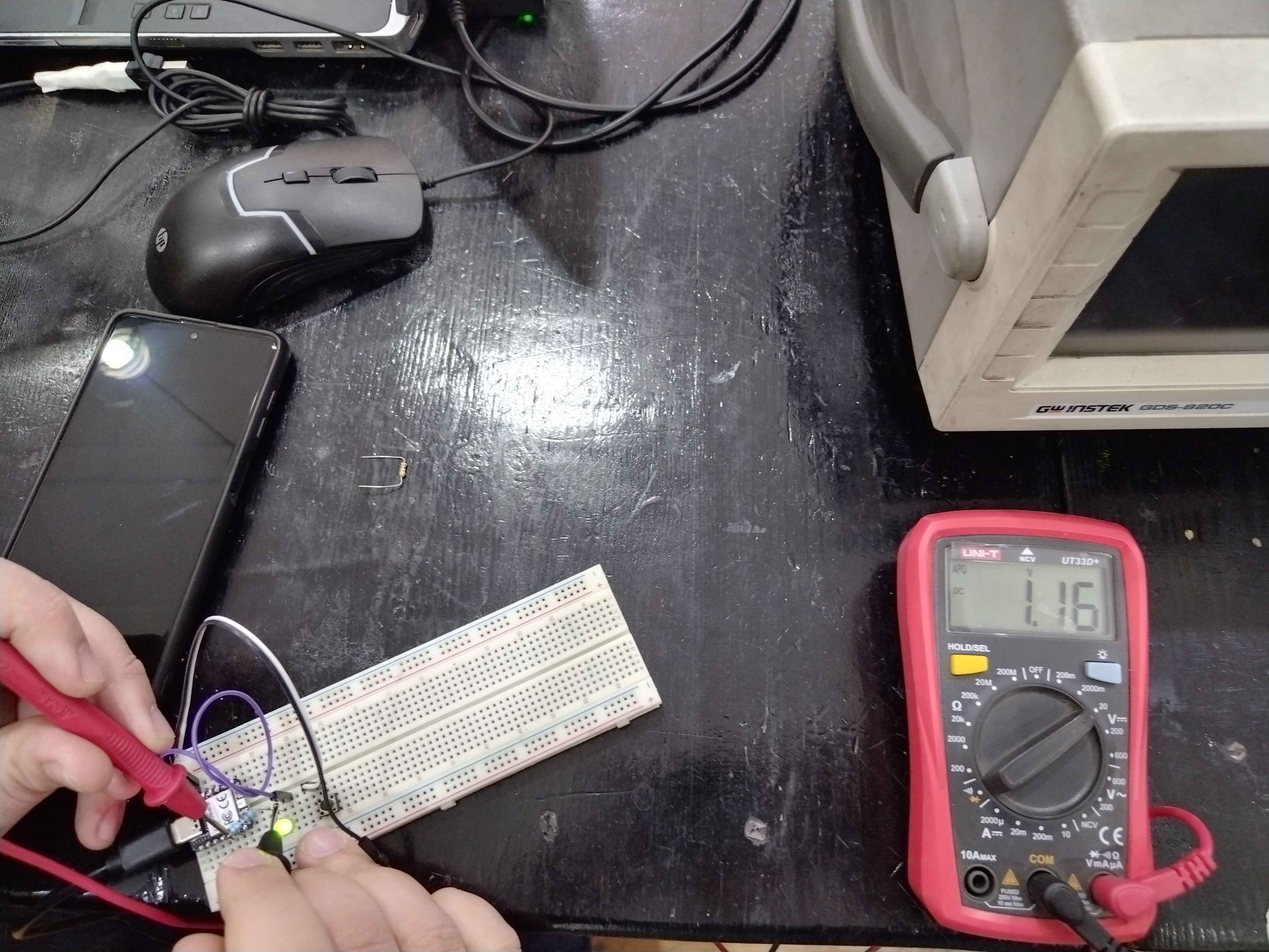
Oscilloscope
Oscilloscope is a type of electronic test instrument that graphically displays varying
signal voltages, usually as a calibrated two-dimensional plot of one or more signals as
a function of time.

We used the Oscilloscope to observe the different out of signal fom the Xiao RP2040.
Multimeter
We also used the Multimeter to check the voltage across the LED legs in example circuit.
And check the resistance value.

Check our
Group assignment page to see more of our assignment.
PCB Design
- First I start by Installing KiCad.
- Then I download Fab Electronics Library for KiCad and followed the installintion instruction to get everting setup.
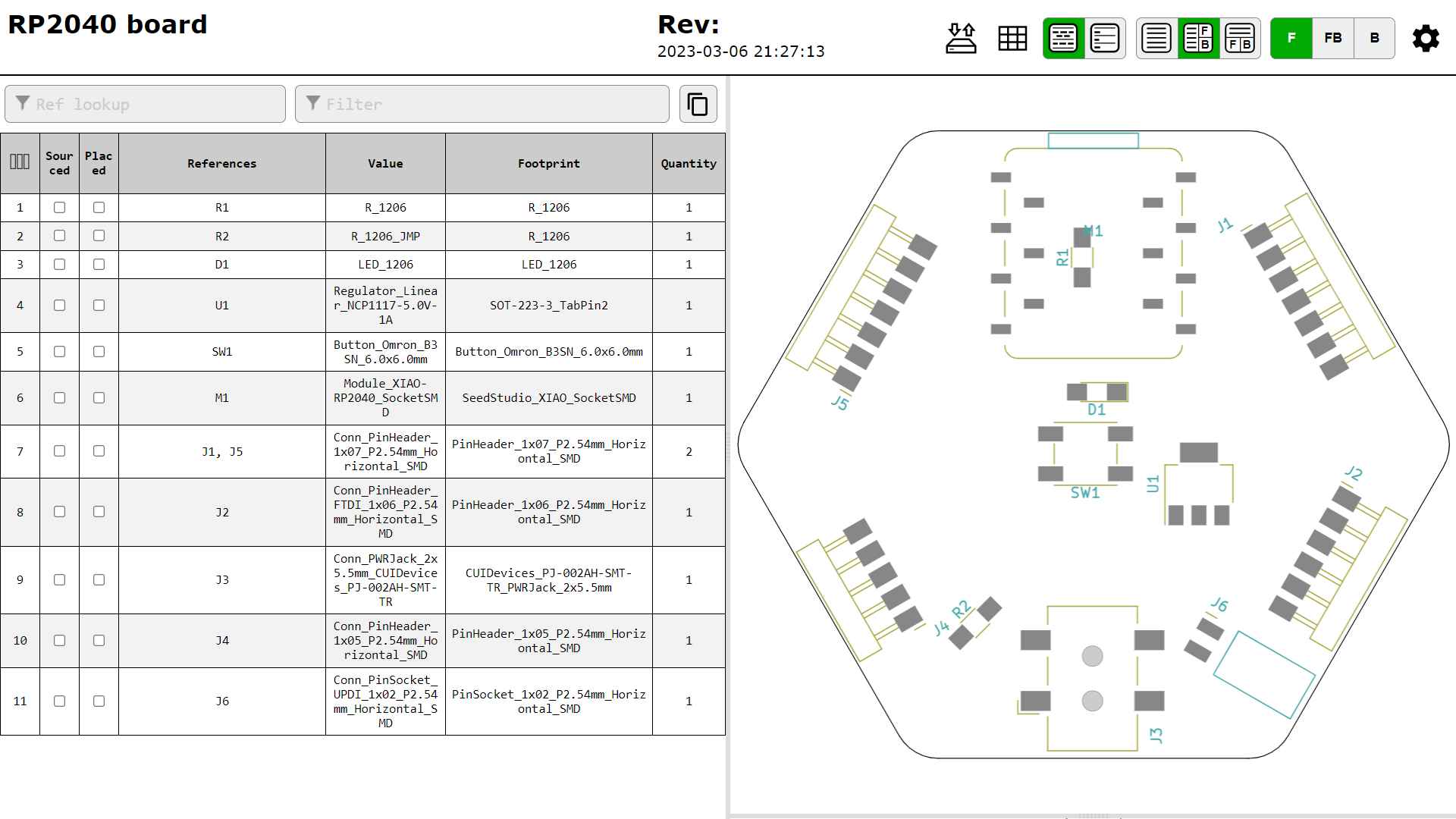
- I also installed Interactive Html Bom plugin to export my Bom after I finshed my design.
- Then I want to make PCB using Xiao RP2040 as my controller.
- I start by making my schematic by adding components symbols wire them together.
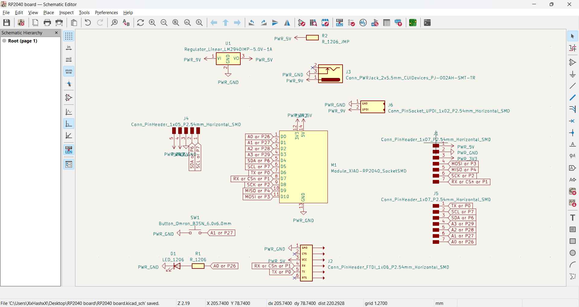
- I checked the ERC it say that I connected power input into power output pin but in the real I would use it for output
- Note: I also check on Seeed website that I could power up the Xiao RP2040 using 5V power source through the 5V pinout.
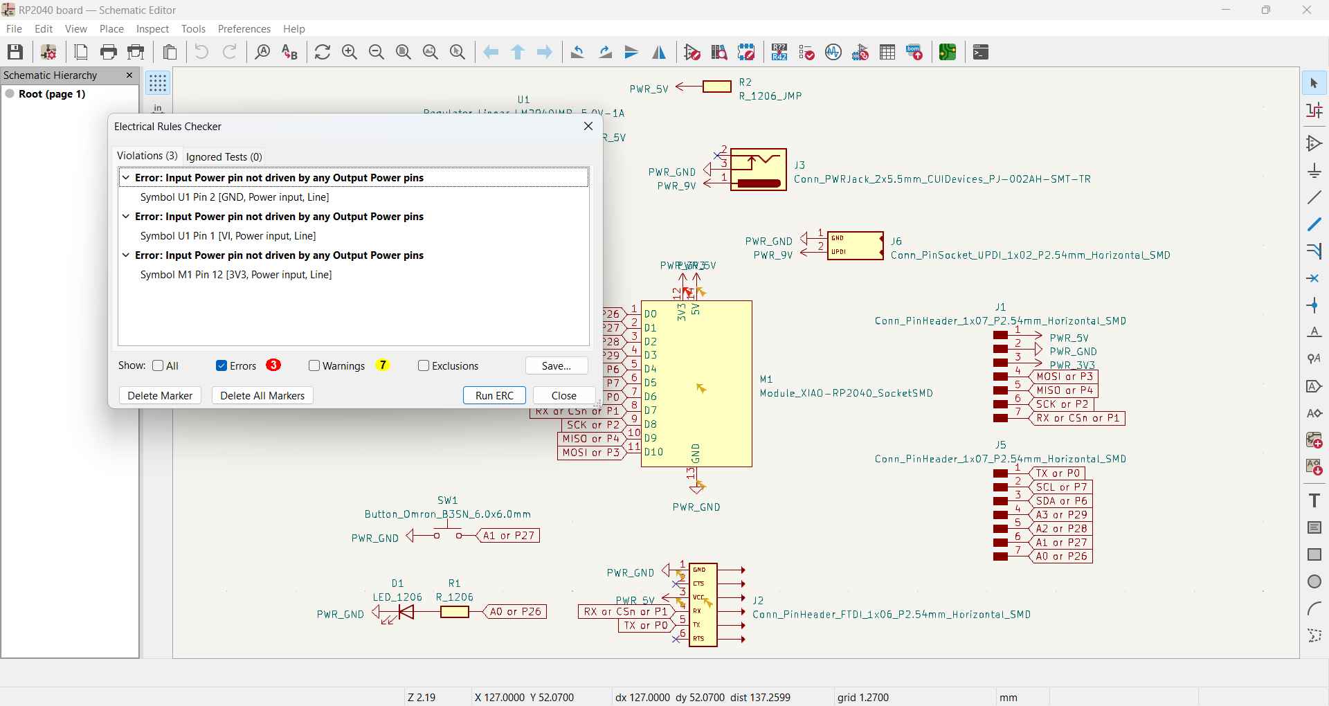
- Then, Annotate Schematic to be able to send the components to the board editor.
- Then, I open the PCB editor and set Desing Rules > Constraints as I have already fabricated PCB using miling machine before so I set the clearance to be 0.5 just to be on the safe side.
- Then, clicked on Update PCB with changes made to schematic
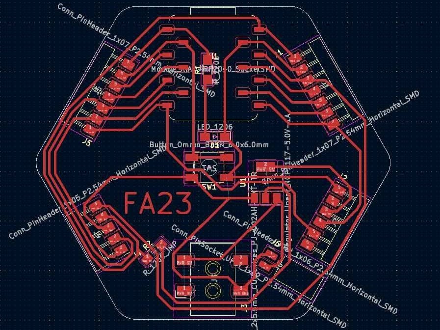
- Then, I start to rearange the components next to each other to have a feel of what they would look like and what will be the shape of the outline.
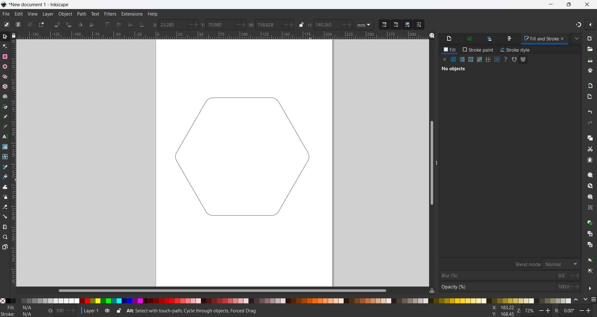
- Then, draw my outline on Inkscape and import graphics the Edge.Cuts layer
- Then, I start routing my components I also had to use 0 ohm resistor to use it as a jumper.
- I also want to try making a common GND so I followed this tutorial

- Then, I checked the DRC and it gives me an error as I have mulitple GND zones separated but if you check you will found that they are all connected via components that has mulitple GDN pad such as the push button and the regulator.
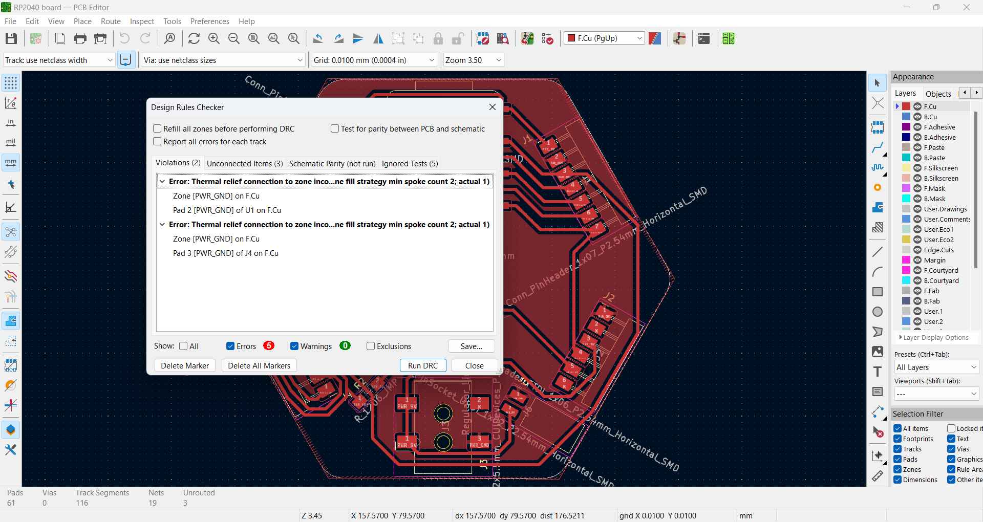
- Finally, I exported my Bom using Interactive Html Bom plugin.