Output devices
Recitation: https://vimeo.com/810678469 Review: https://vimeo.com/812971474 Slides: http://academy.cba.mit.edu/classes/output_devices/index.html
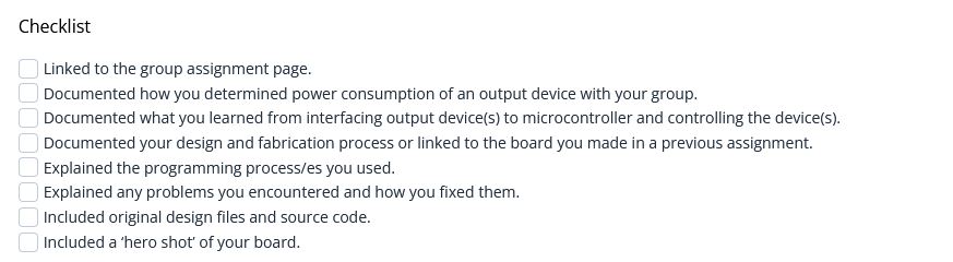
Group assignment:
- Measure the power consumption of an output device.
- Document your work on the group work page and reflect on your individual page what you learned.
Individual assignment:
- Add an output device to a microcontroller board you’ve designed and program it to do something.
Files
Servomotor control signal
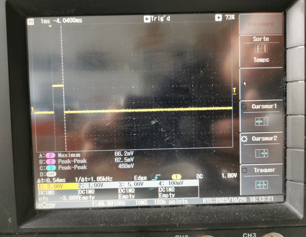
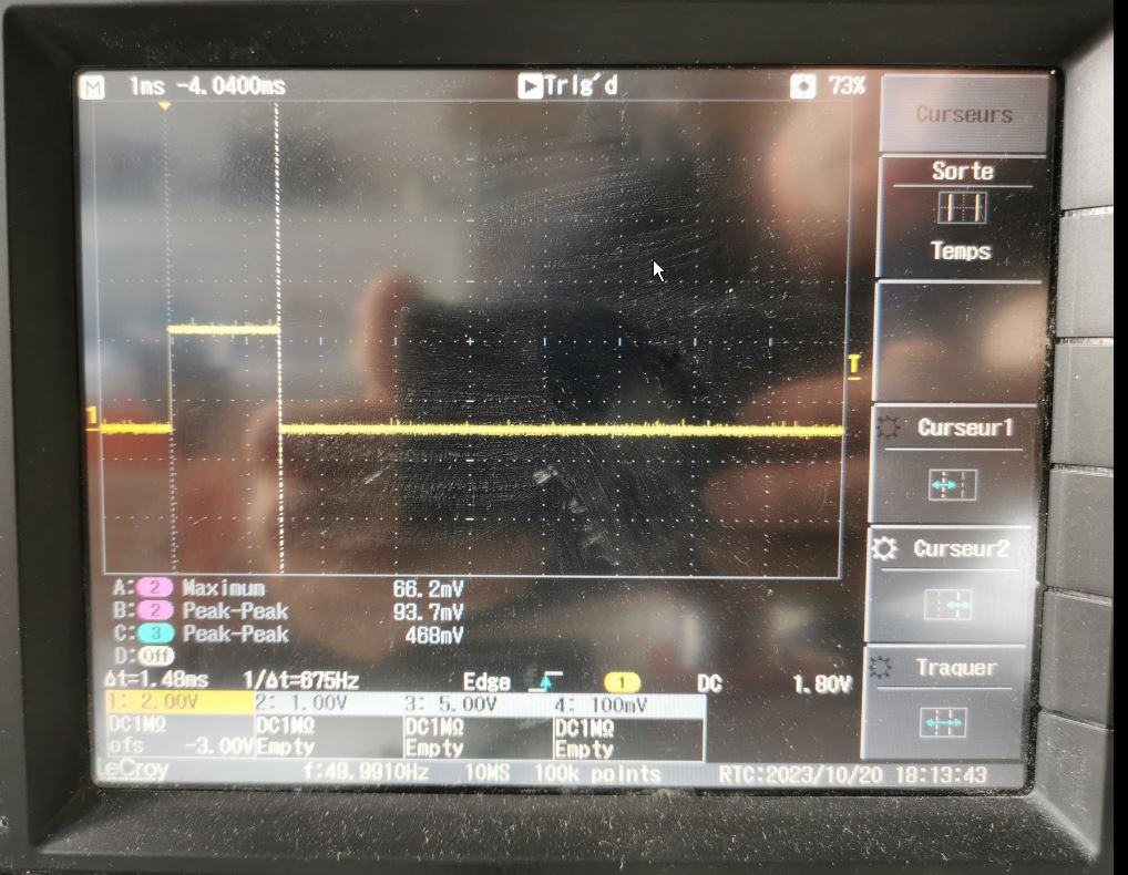
For the group assigment, I observe the output signal of an arduino pin using servo.write(XX) method of the standard arduino <Servo.h> library.
| Servo command at 0° | Servo command at 90° | Servo command at 180° |
|---|---|---|
 |
 |
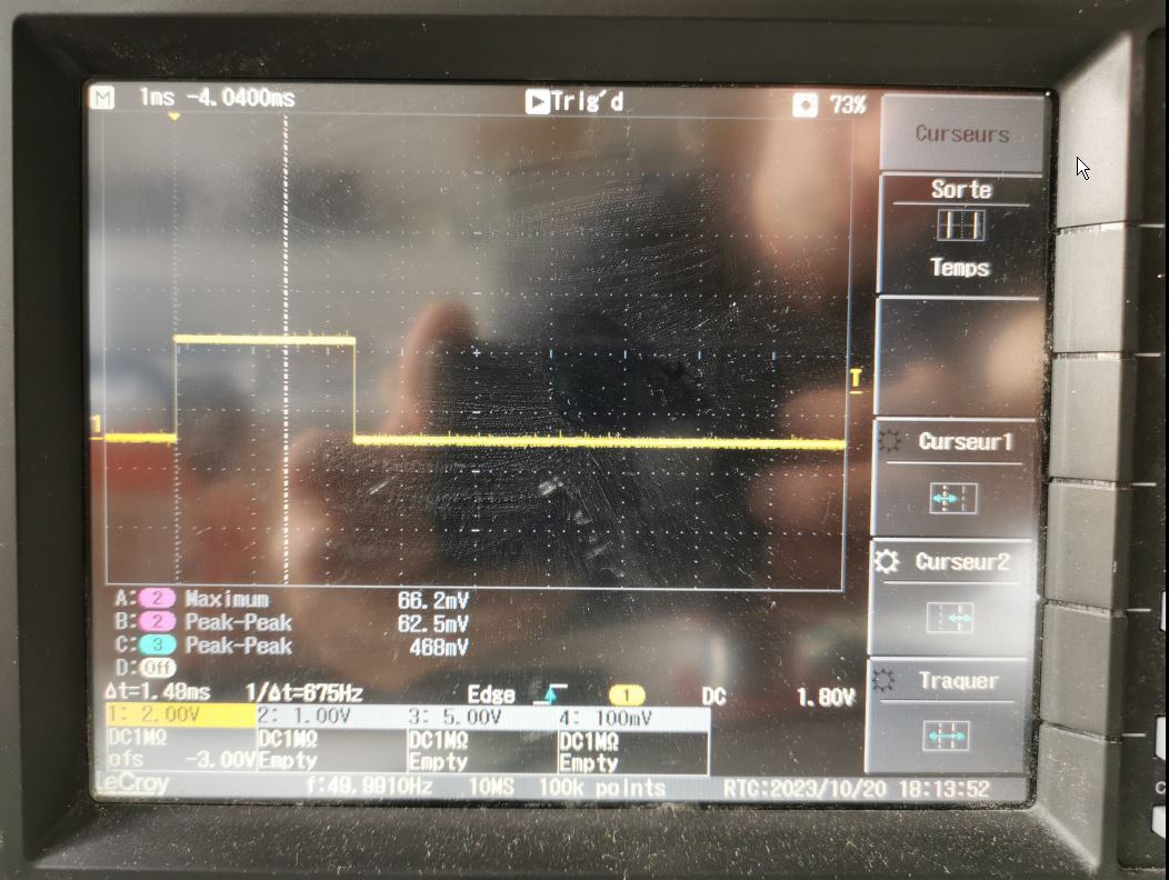 |
I connect a probe to ground and another to signal output of the arduino. I measure a step signal of 0.54ms, 1.48ms and 2.38ms for 0°, 90° and 180°.
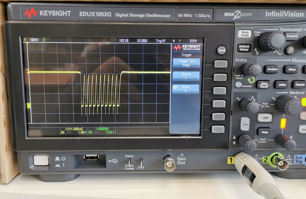
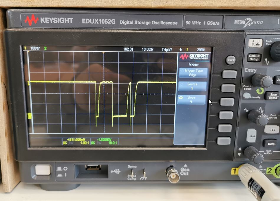
Now let’s check the signal of an I2C output (after initialisation of i2C thought SSD1306 oled screen example).
| SCL signal | SDA Signal |
|---|---|
 |
 |
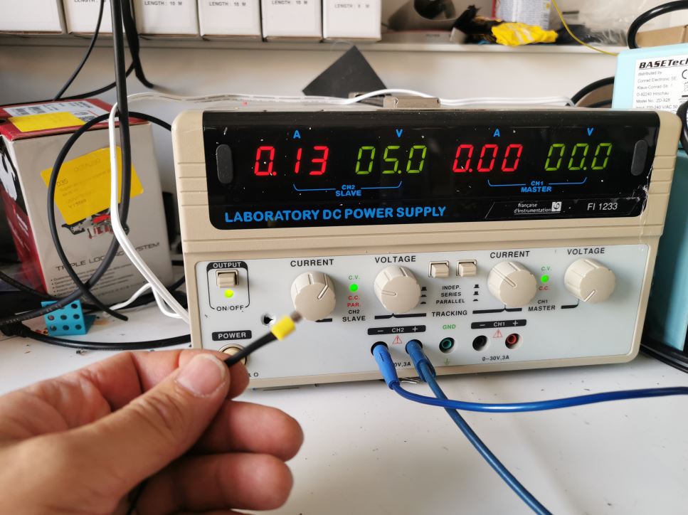
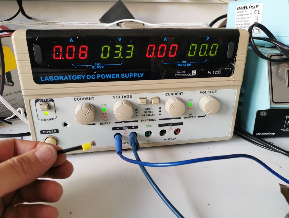
Monitor power consumption
To measure the power requirement of an output device, we can use a multimeter in serial with it. Our power supply also has a power indicator. Supplying current for a small vibration motor, I appear to consume 130mA at 5V and 80mA at 3.3V.
| Power at 5V | Power at 3.3V |
|---|---|
 |
 |
Creating the PCB
Oled display into Kicad
I need to include footprint and schematic for Adafruit Oled display 128x64. I didn’t found a version for Kicad 7, so I will create it from documentation:
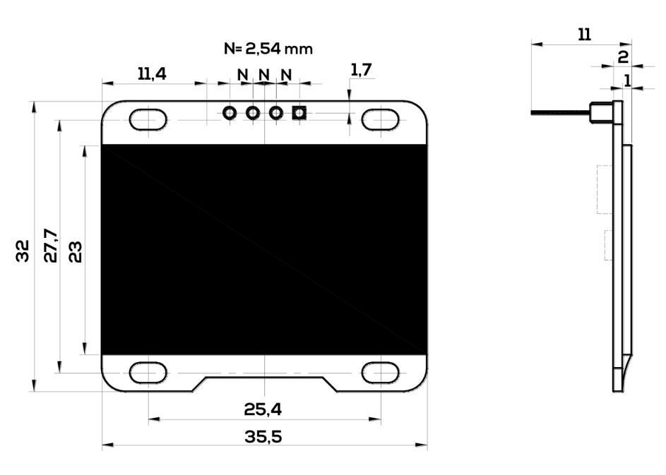
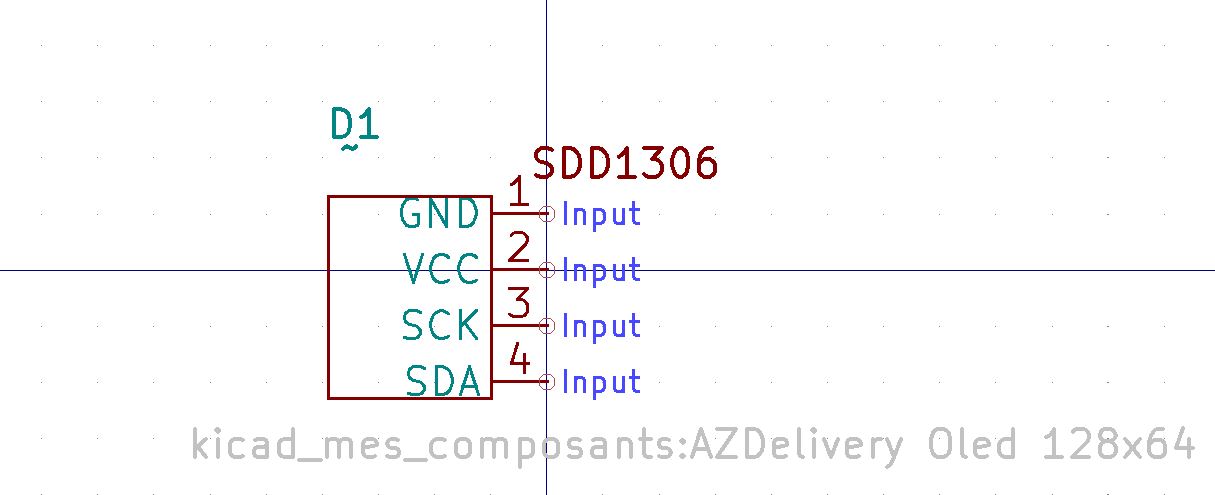
Pins are, from left to right: VCC/GND/SCK/SDA SDA for Serial DAta SCK for Serial Clo**CK* (can be found as SCL for Serial CLock)
The I2C adress is 0x78, note that it can be changed if we need 2 displays on the same i2c bus or if it is conflicting with another i2c device. Simply change the position of the smd resistor on top-left. Note: When jumper is set to 0x78, use 0x3C in code, when jumper is set to 0x7A, use 0x3D in code. (see this thread for information about this (forum).
Step File for 3D preview is available here: https://grabcad.com/library/ssd1306-oled-display-128x64-1
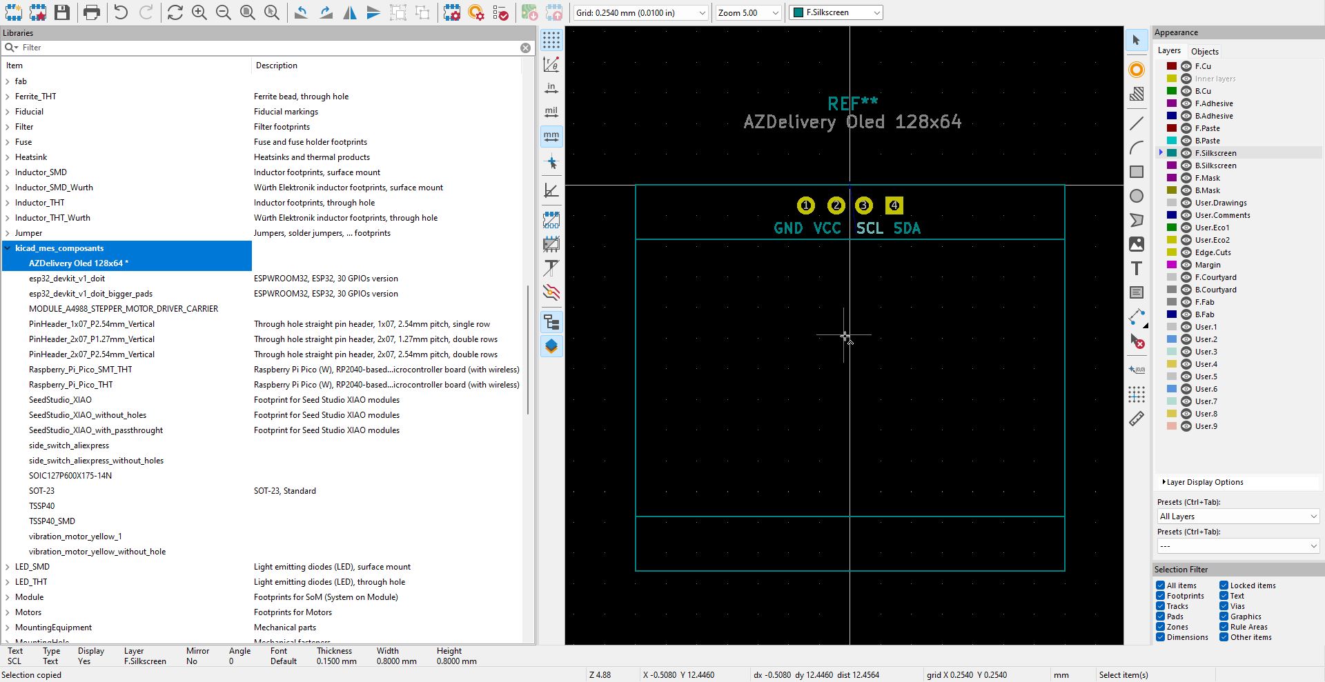
In Kicad, Symbol editor, Tools > Symbol editor. Then select a library where you whant to record this component. For me it’s “kicad_mes_composant”. Then click on “create a new symbol” button on top-left. Draw the symbol shape, add pins and names. Don’t forget to assign a pin number to each of them.
Note: Puting one of the pin to origin and placing all the pin in a 2,54mm grid simplify connection into board schematic later.
Now on Footprint Editor, select the working library as above and click on “Create a new, empty footprint” button on top-left.
Select grid size at 0.5mm, then draw outlines. Use properties of component and positioning tools to place lines and pads at the exact positions. Note that it help a lot to place the component origin on a corner or middle of the component.
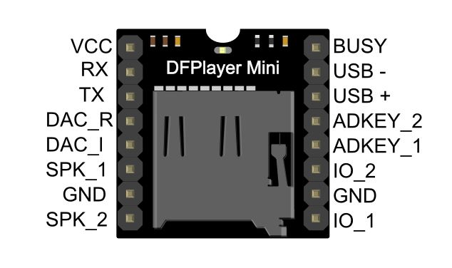
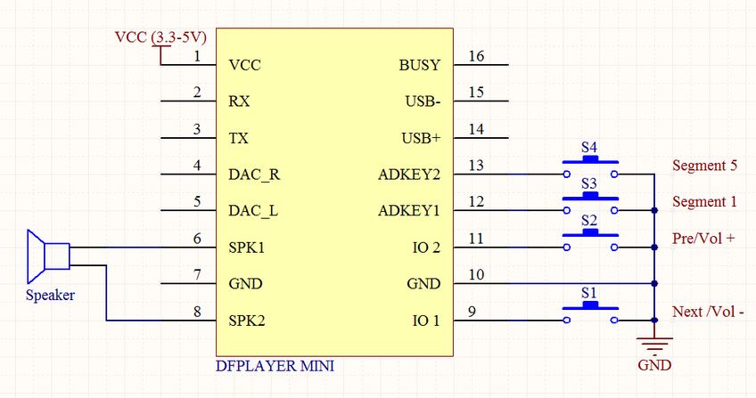
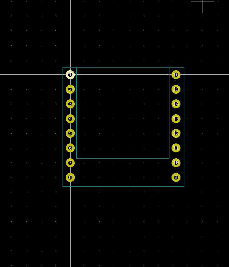
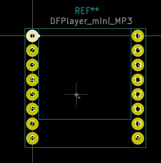
MP3 player into Kicad
I follow the same stps to create the MP3 reader component (DFPlayer mini) I found some ressources here: https://wiki.dfrobot.com/DFPlayer_Mini_SKU_DFR0299
A typical schematic is:
I didn’t found the board dimentional drawing, so I take measurement by myself.
| 1 | 2 | 3 |
|---|---|---|
 |
 |
 |
| symbol | schematic |
|---|---|
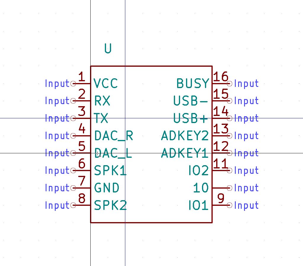 |
 |
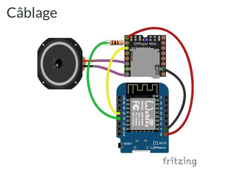
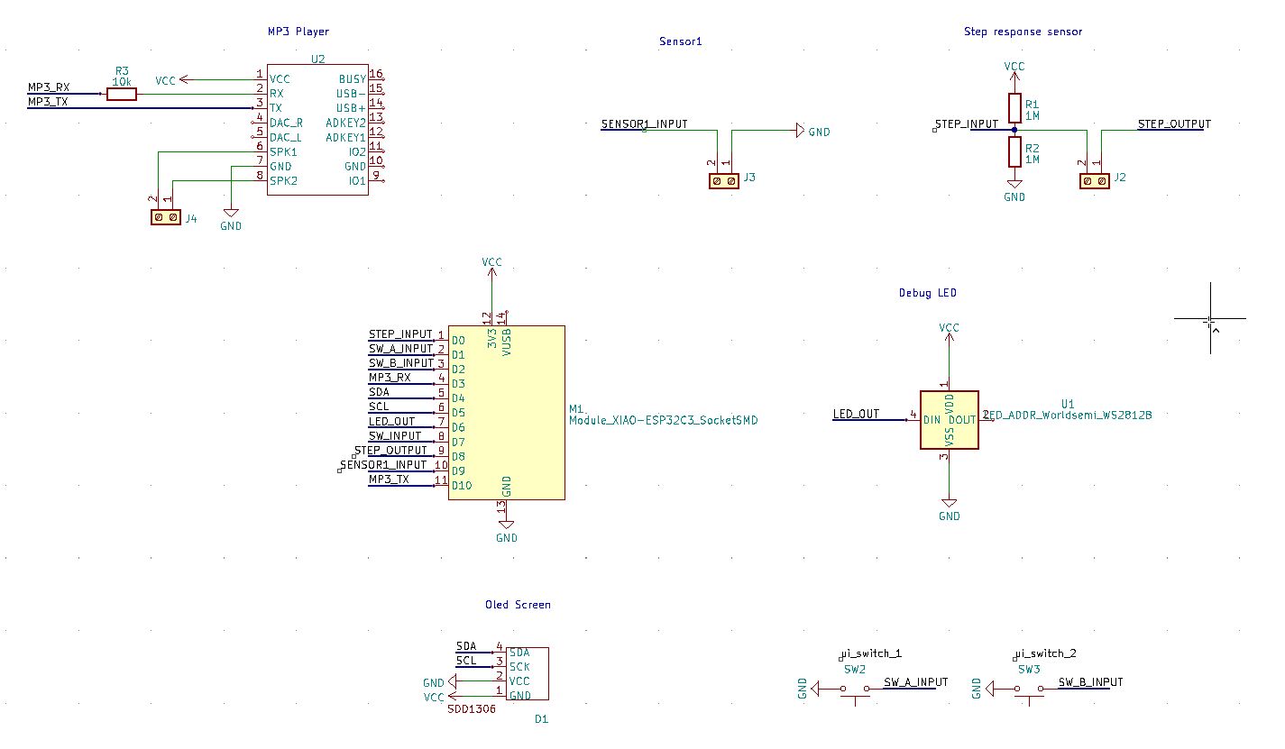
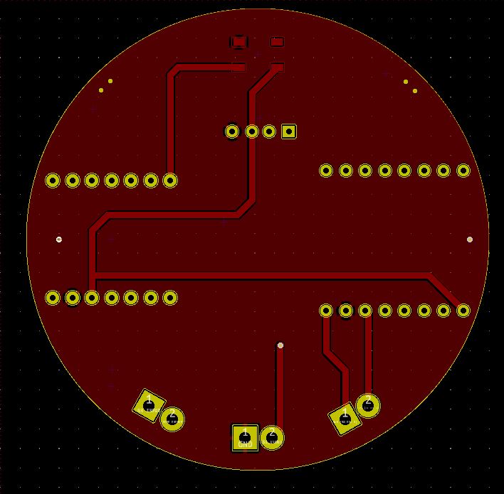
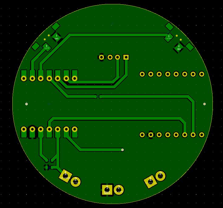
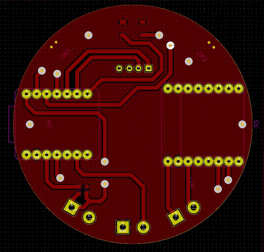
Board Schematic
For the board, I add the folllowing components:
- Oled screen
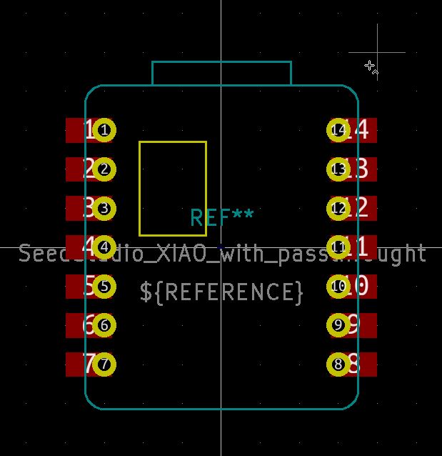
- esp32c3 xiao
- 1 ws2812b led
- 2 switches for user interface
- 3 terminal blocks for sensors and speaker connection
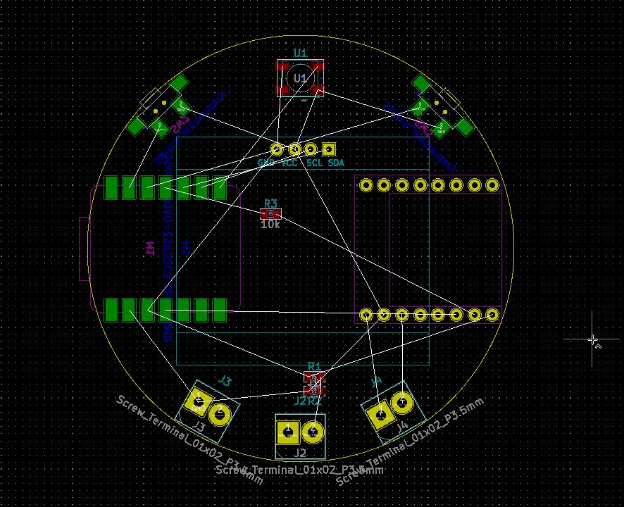
Making the PCB
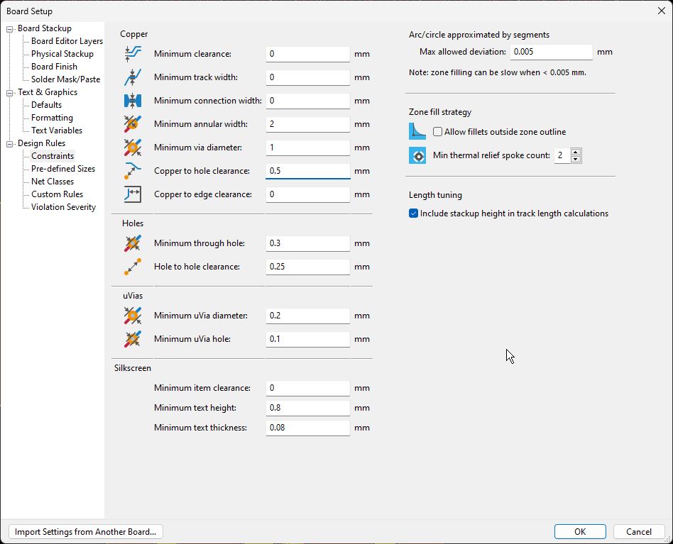
I place the components on both side of the board. I will include 2 drill holes to align after flipping during manufacturing. I position them along the same y position. To go from one side to the other, passthrought component act as vias. To add other vias, I use 2mm as via diameter and 1mm as via hole, I will then solder a piece of wire inside to make the connection.
I use a ground plate for this board, To make tracks easily trace with our cnc, we have to adjust tracks clearance:
| Top layer | Bottom layer |
|---|---|
 |
 |
Preparation for PCB milling
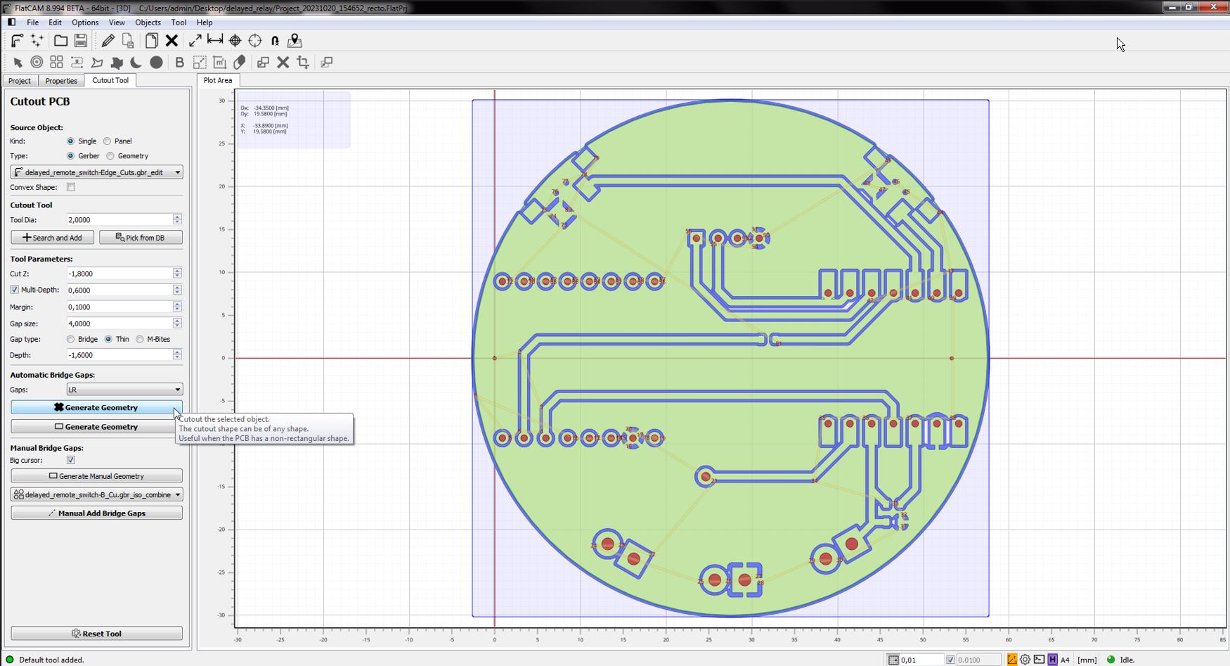
I will use FatCAM to convert my gerber to nc file for our SRM-20 cnc. I load Top and bottom layer gerber file and xxx-pth.drl excellon drill file.
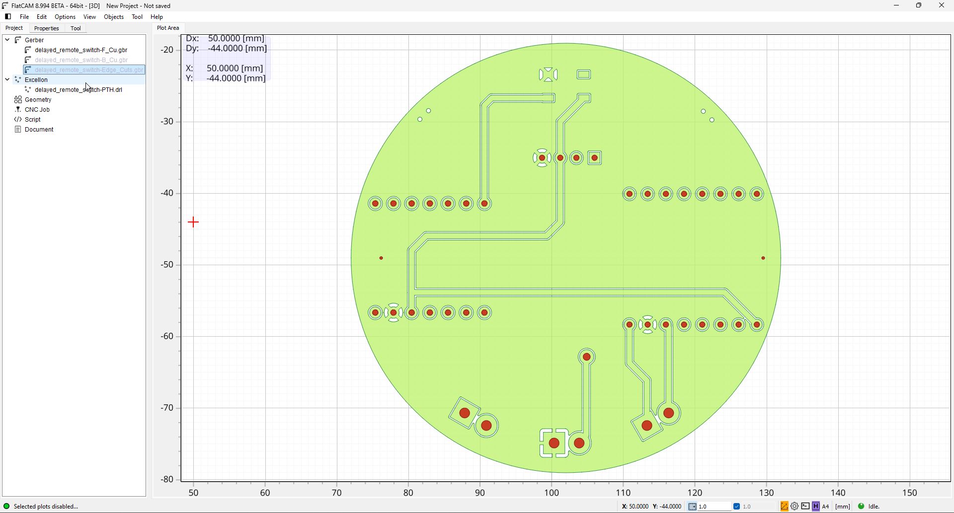
I double-click on top layer on left explorer, Tools>Isolation routing. Then select the right tool by clicking on “Pick from Database”
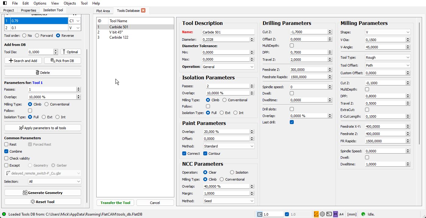 We can select or create a new tool. Then select it and click on Transfer the Tool.
I choose 1 for number of pass because it is faster to manufacture, but we can choose 2 or 3 pass to simplify soldering.
Now click on Generate Geometry.
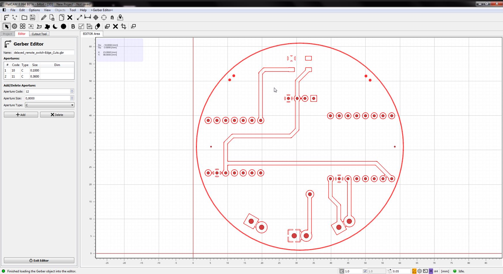
Edge cut
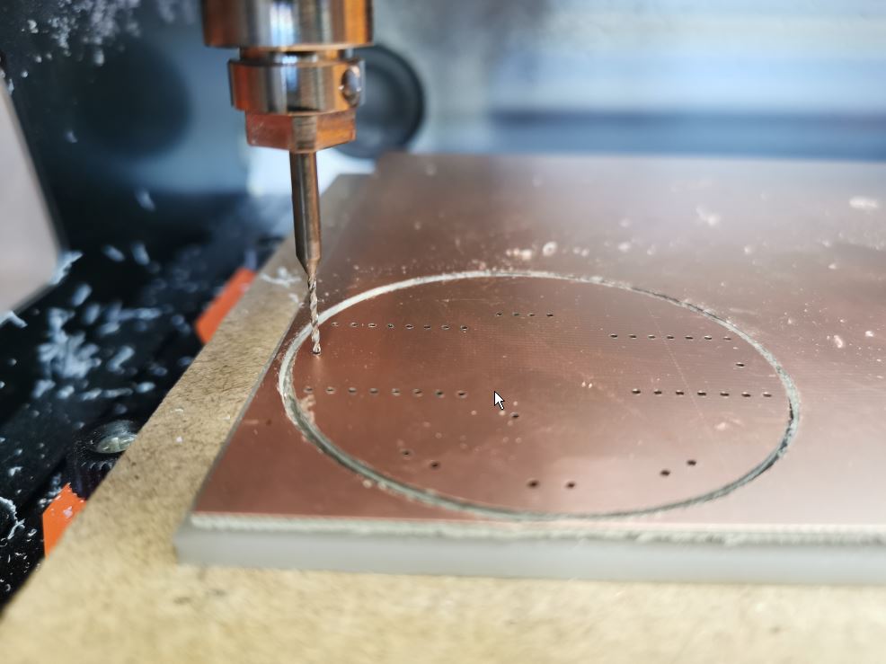
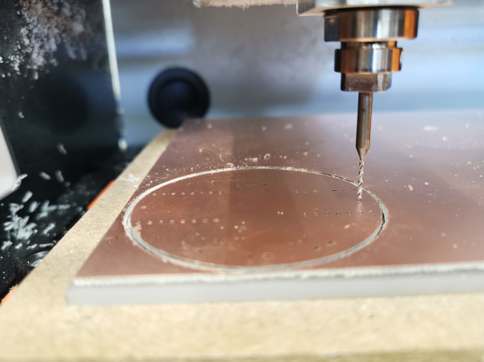
Flatcam doesn’t like when there is multiple geometries in edgecut layer. Here for example, we have some “parasite” holes that are on this layer. We can remove theme from KiCad side or by editing gerber inside FlatCAM, select unwated items , delete them, exit editor and save. Then use the edited gerber for edge cut, double click on it. Go into cutout tool section, select and transfer the correct tool (Carbide #122 in my case) and Generate geometry. Then choose the proper thickness to cut (my pcb is 1.7mm thick, I choose 1.8mm), then Generate CNC Job and Save CNC job.
Two side engraving
Preparation
The process to do 2 side pcb on SRM-20 is the following:
For the PCB:
- Engrave traces in side 1
- Cutout the edges of the board
- Drill the holes
- With a ruler, align with the 2 aligment holes and draw a mark with a marker on the side of the rest stock.
- Return the board (left side go to right side), and align with the mark. Keep it in place with double tape.
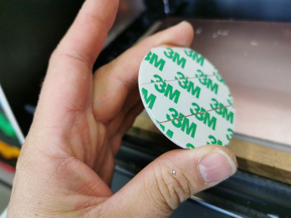
| Put a mark before flipping | Then align with the line’s edges |
|---|---|
 |
 |
- Reset the XY origin to the center of the left hole, reset the Z origin on the surface of the board. You can move on x axis only to check that the bit align with the right hole too.
| Set origin at hole center | check for good aligment on right hole |
|---|---|
 |
 |
From FlatCAM:
- Select bottom and excellon layers
- Flip on X axis (miroring)
- Zoom on maximum on the left hole and set origin at it center. Note: Be carreful to decrease grid size for accurate positioning, I choose 0,01mm
- Generate Geometry and CNC Job for bottom layer as previously
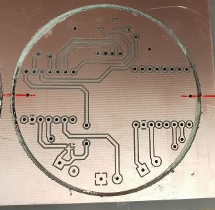
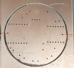
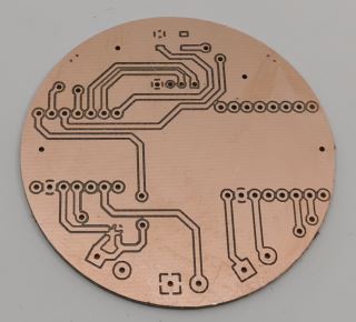
Result
| Top layer | Bottom Layer |
|---|---|
 |
 |
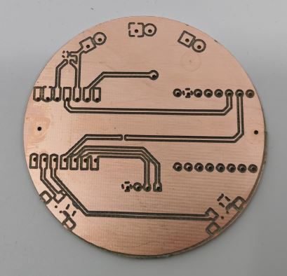
Alignment and engraving are quite good, but I found several problems:
- Traces could be bigger, I will chose 1mm width instead of 0.8mm when possible.
- It is impossible to solder pin under oled screen, esp32c3 and DFPlayer! I have to redo the board in such a way that no traces has to be connected on those component side, but on the other. If it is really mandatory to have a trace on component side, I will make it go outside of the component and not under it.
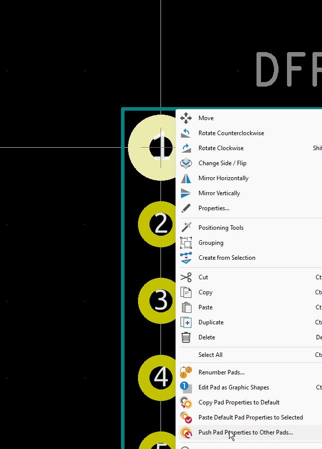
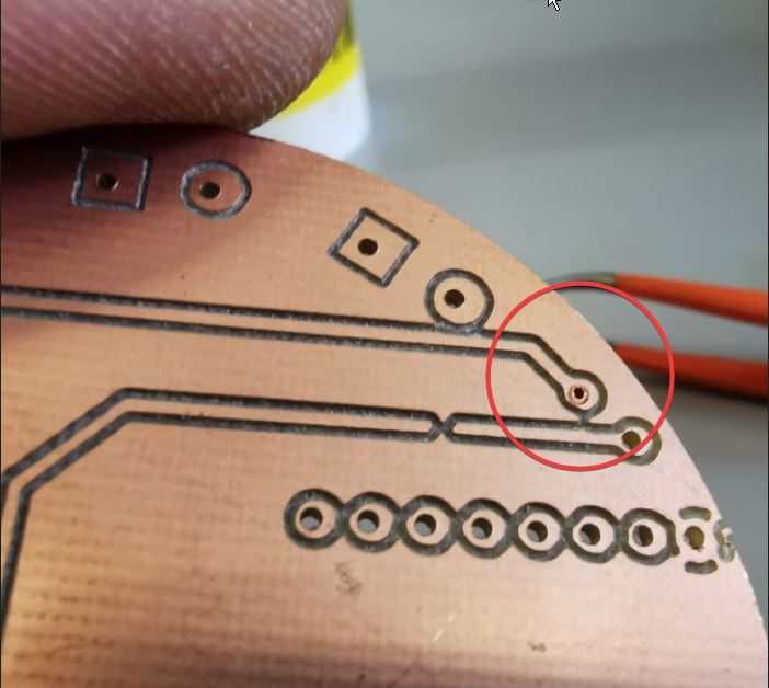
- The pads are too small comparing to holes diameter, there is no place for the solder! I will change those diameter to make them as big as possible (from 1,525mm to 2.2mm).
In Kicad footprint editor, a tool allows to do this easily. Change one pad property, then right click>Push Pad Properties to Other Pads…
| Before | After |
|---|---|
 |
 |
| Before | After |
|---|---|
 |
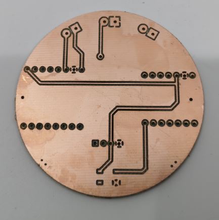
Second trial
Making the PCB
| Top layer | Bottom layer |
|---|---|
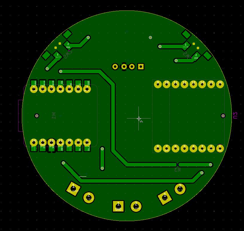 |
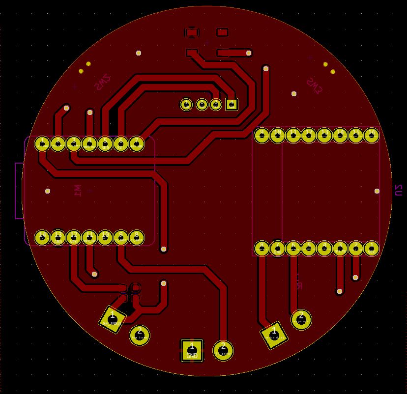 |
After another milling, I realized that the vias size has to be changed too! I now set via diameter to 2mm and via hole to 0.8mm.
| Top layer | Bottom layer |
|---|---|
 |
 |
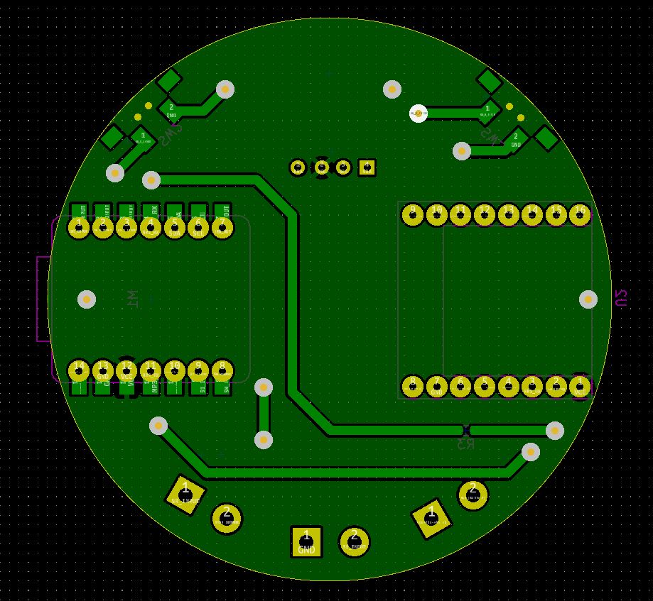
Result
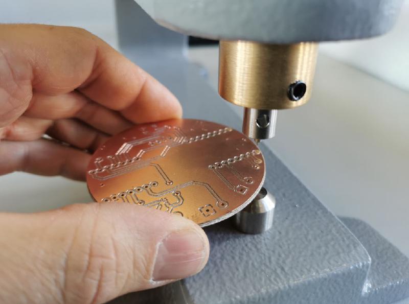
Raw PCB
It’s better! There should be more space for soldering now.
| Top layer | Bottom Layer |
|---|---|
 |
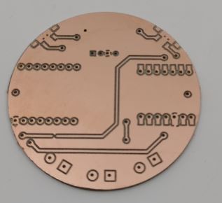 |
Adding vias
At our lab, we have a tools to insert vias into pcb, It act as riveting machine.
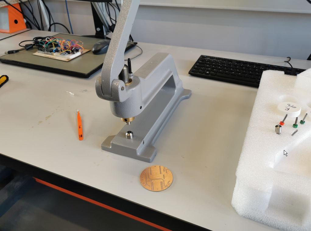
The board on the left and via on the right:
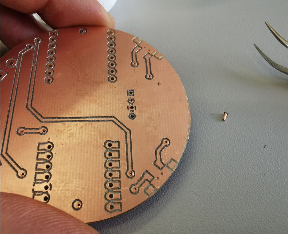
Riveting in progress!
 Closup on the inserted via:
To complete the process, we now have to put some solder on it to secure them.
A little word on soldering
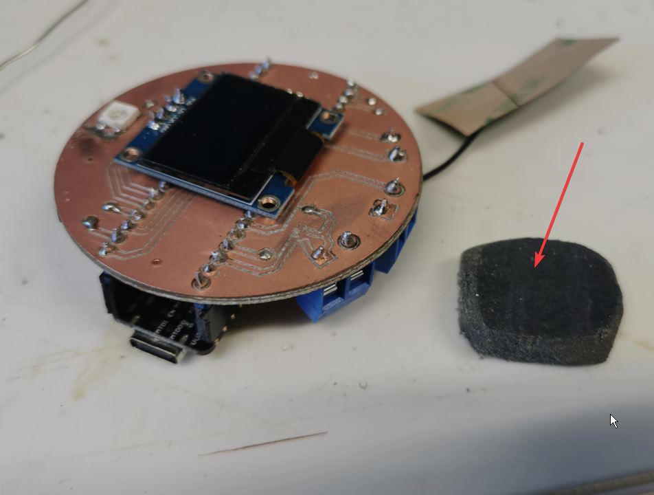
I found that is is very tedious to solder a “Lab made” board compared to board ordered to PCB manufacturer. The solder doesn’t stick well on the pads, this can be due to finger grease or oxydation of the copper. A colleage show me that those 2 problem can be remove thanks to a “pcb eraser” (pcb eraser), just “erase” the pads of the pcb before soldering and it make it perfectly clean, letting the solder flow far more effectively.
Board with components
| Top layer | Bottom Layer |
|---|---|
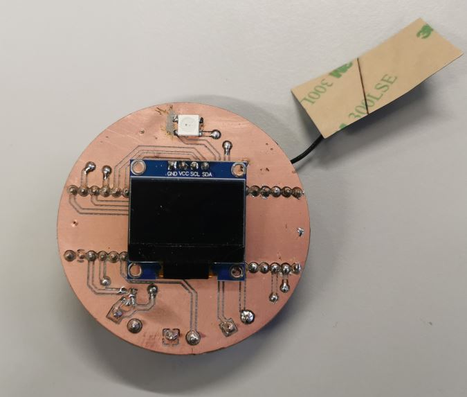 |
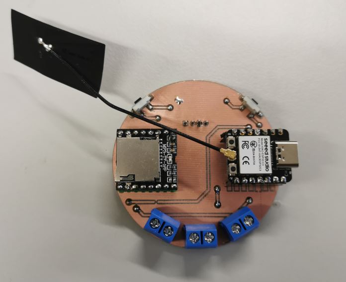 |
Testing the board
Arduino program
You can find the arduino code here: code
I combine:
- Step response code from Robert Hart [step reponse] (https://roberthart56.github.io/SCFAB/SC_lab/Sensors/tx_rx_sensors/rx_tx03.txt)
- Oled demo code from Adafruit_SSD1306 libray
- DFRobotDFPlayerMini: https://www.wikidebrouillard.org/wiki/Item:DFPlayer_Lecteur_MP3
- FastLed, Blink example code