Slides: http://academy.cba.mit.edu/classes/electronics_production/index.html Recitation video: https://vimeo.com/808514185
-
Group assignment:
- Characterize the design rules for your in-house PCB production process: document feeds, speeds, plunge rate, depth of cut (traces and outline) and tooling.
- Document your work to the group work page and reflect on your individual page what you learned
-
Individual assignment:
- Make and test the development board that you designed to interact and communicate with an embedded microcontroller
Learning outcomes
- Described the process of tool-path generation, milling, stuffing, de-bugging and programming
- Demonstrate correct workflows and identify areas for improvement if required
Have you answered these questions?
- Linked to the group assignment page
- Documented how you made (mill, stuff, solder) the board
- Documented that your board is functional
- Explained any problems and how you fixed them
- Uploaded your source code
- Included a ‘hero shot’ of your board
Tools description
-
French supplier for endmills: https://eu.robotshop.com/fr/collections/machine-accessories
-
carbid 501
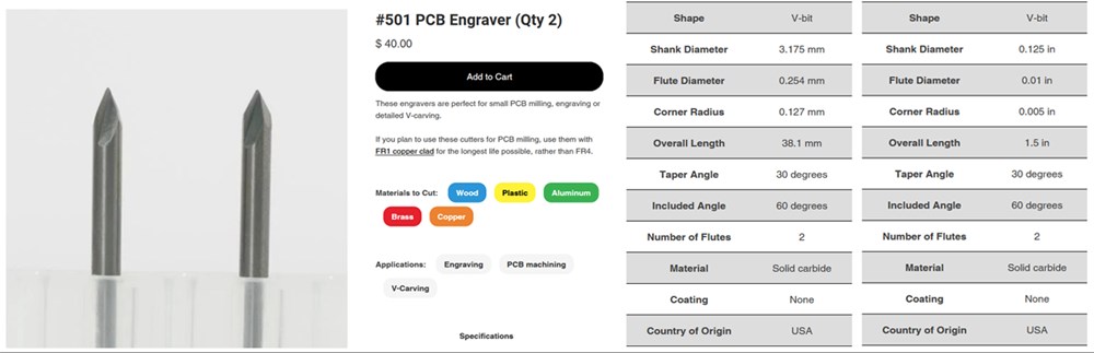
- carbid 104
ServoMotor controler board
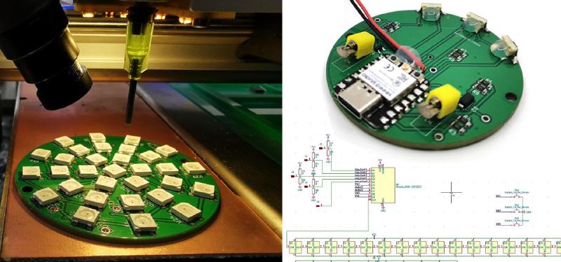
This week, I will mill the PCB designed in week 6, in a second time, I will mill my final project PCB.
Preparation
Mods
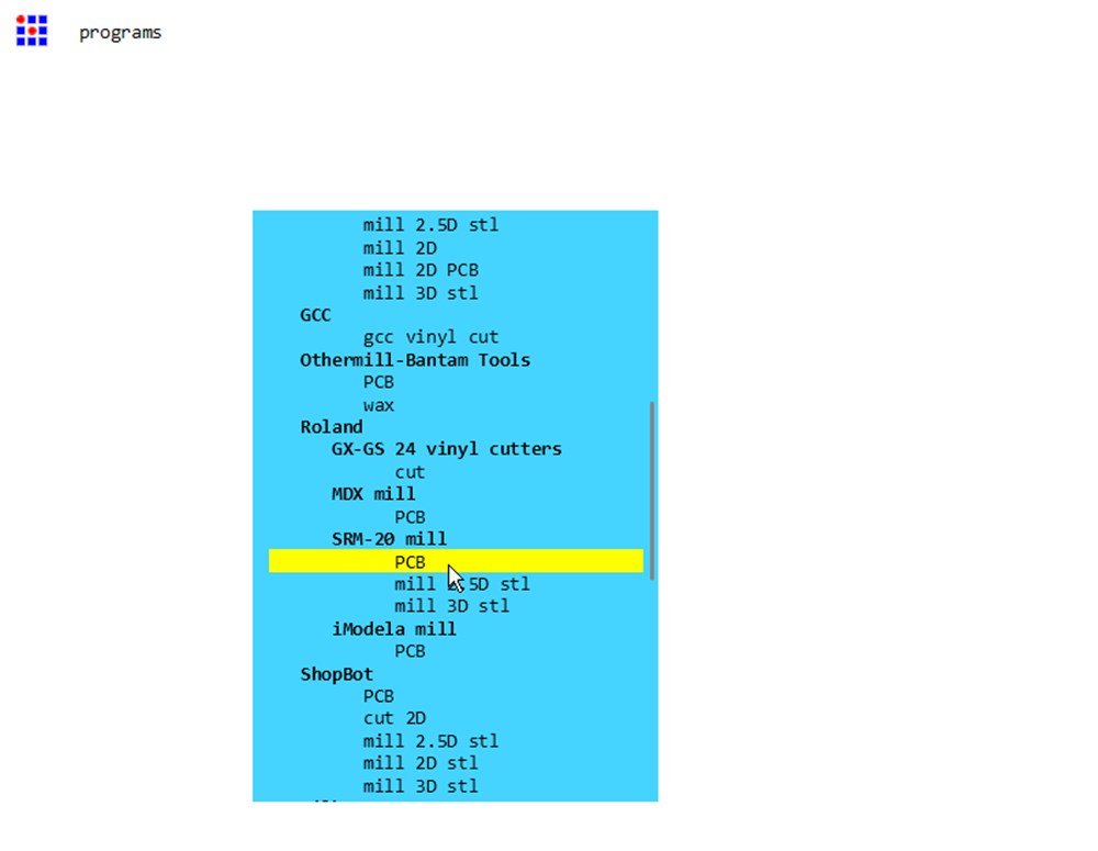
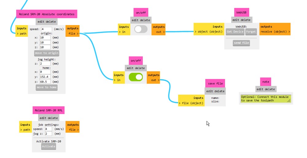
We can generate milling path with Mods software. We use the community edition available here: https://modsproject.org/
Right click> Program>Open Program>Machines>Roland> SRM-20 mill >PCB
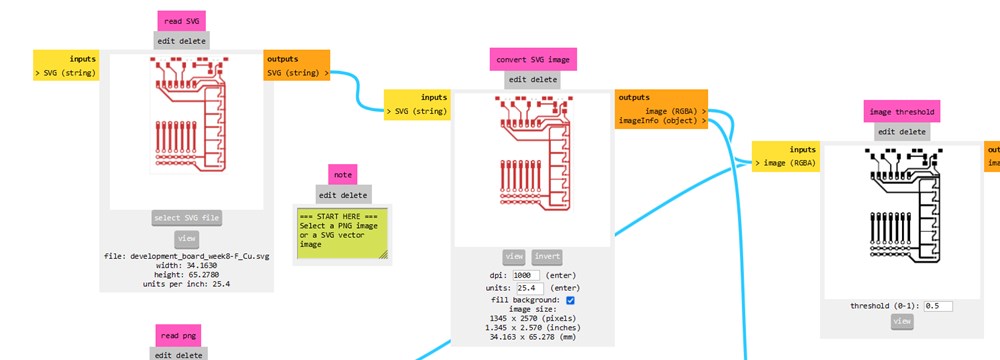
Into Read SVG box, select the file exported from KiCad describing the traces. Check the coherence of width and height with the physical size of the board.
Now set the tool parameters:
- For traces, as we use a 1/64 inch flat tip, we click on “mill traces (1/64)”
- If we use a V-bit, we can use the V-bit calculator setting tip diameter and angle, then click on send calculated settings.
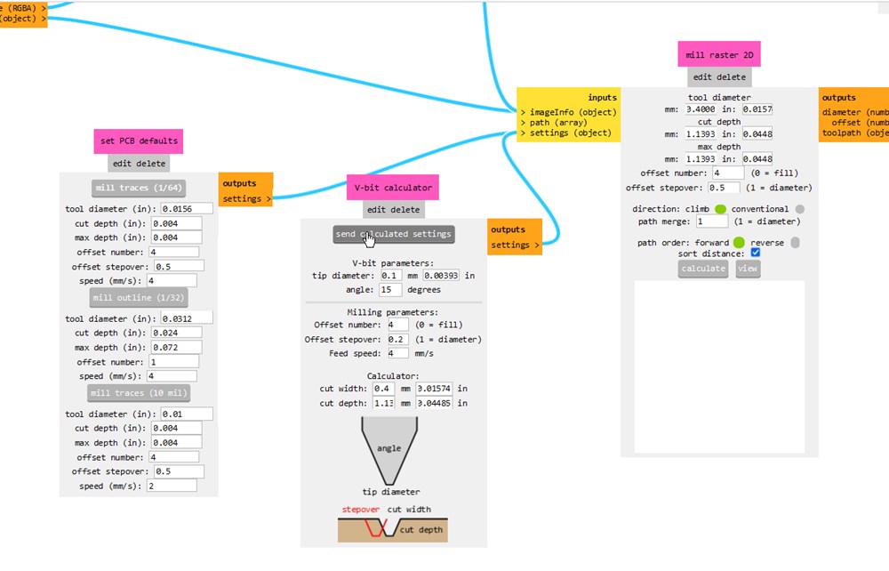
Both boxes update parameters inside “mill raster 2D”. Now click on “calculate”. We can check the result clicking on “view”
To create a rml file, compatible with ou SRM-20 machine, enable the switch going to “save file” and disable the one going to WebUSB.
Click again on “Calculate” to create the file and dowload it automaticaly.
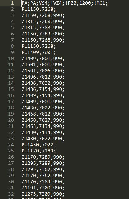
A few lines of the rml file.
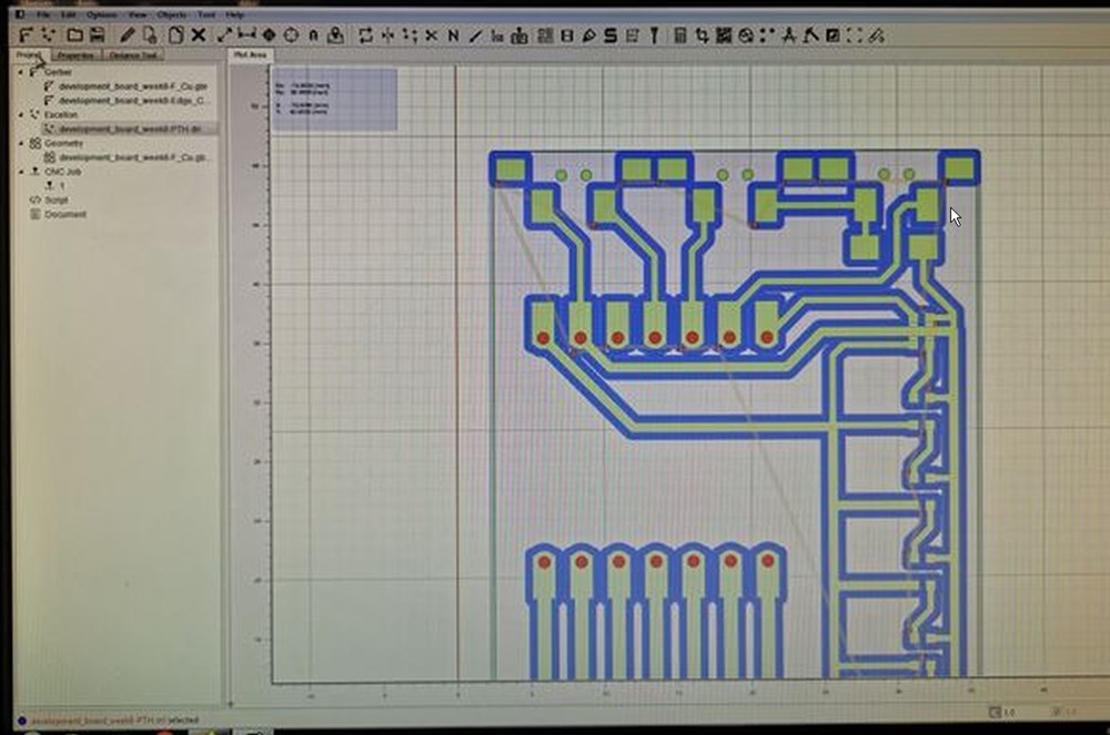
FlatCam
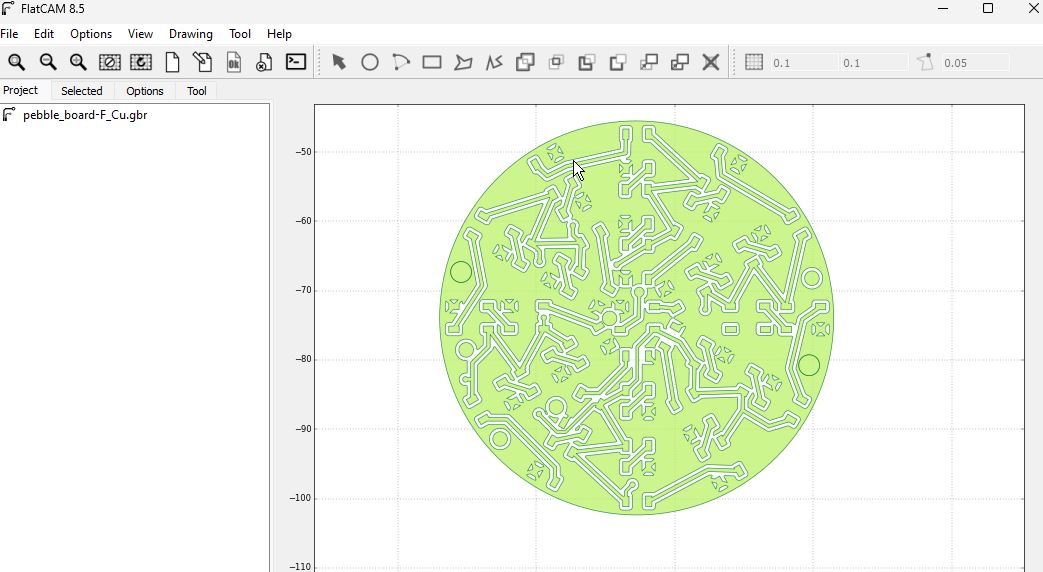
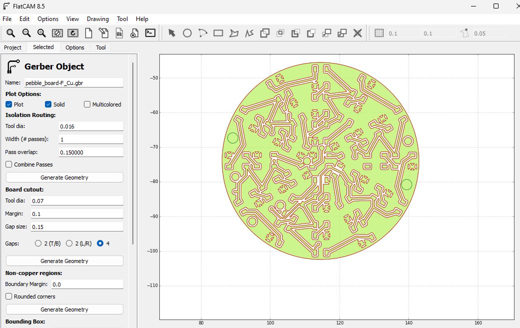
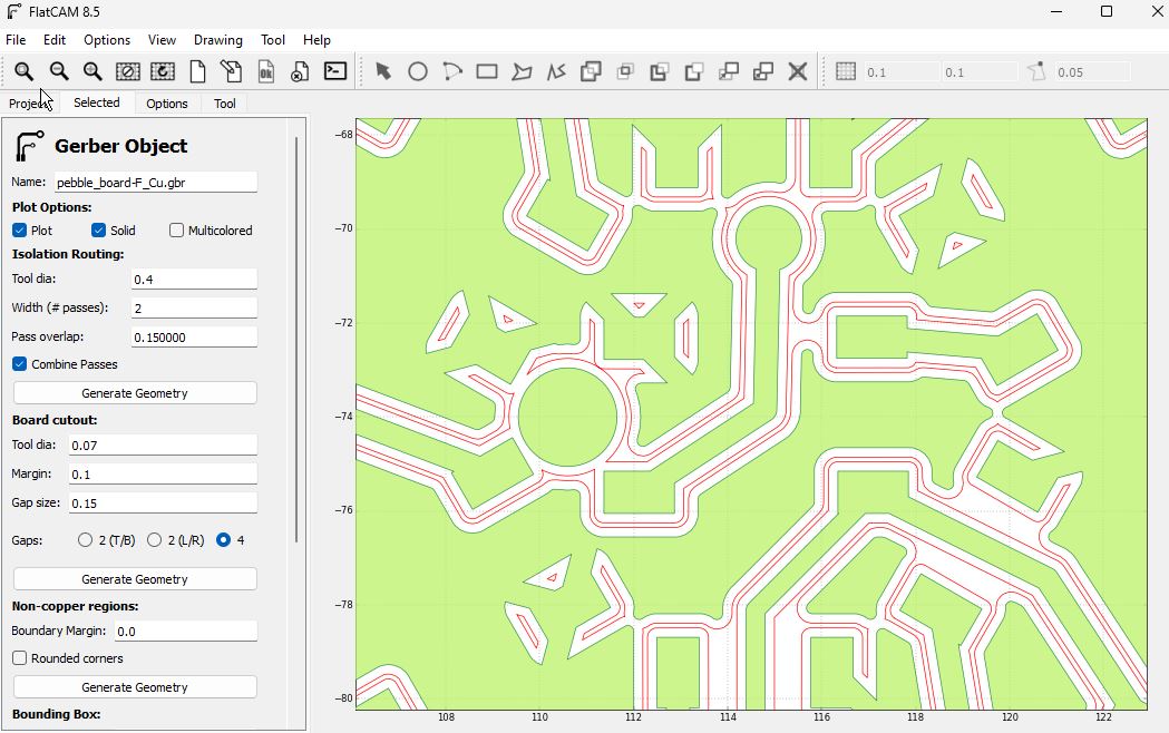
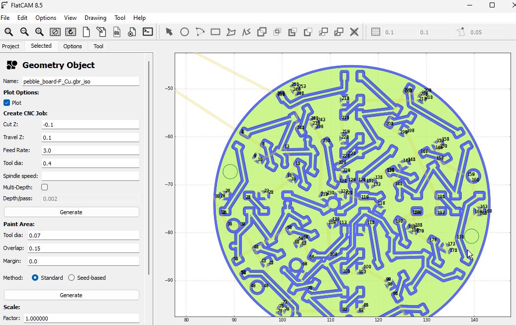
Instead of mods, I prefered to use FlatCAM. It is an opensource software to convert grbl files to CAM. I find it to be quite intuitive and powerfull. The main conterpart is that it doesn’t seems to be actively maintained anymore.
Bellow is a snapshot of the FlatCAM interface, in red, the geometry generated for traces and pads isolation, in blue, the “CNC job” wich is the path of the bits that will be send to our CNC machine.
To export this path, Double click on the CNC job, and Export G-Code
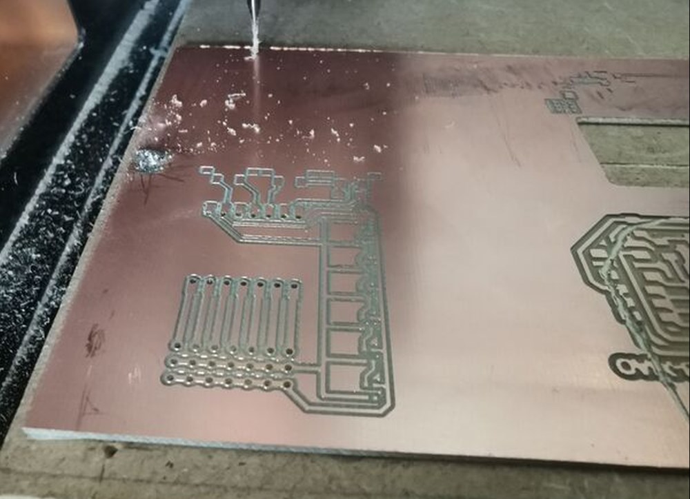
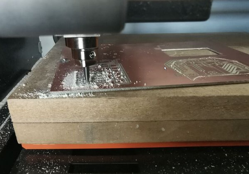
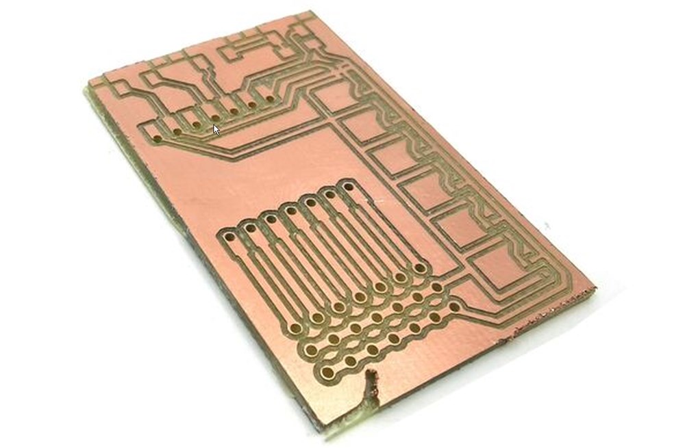
Milling traces
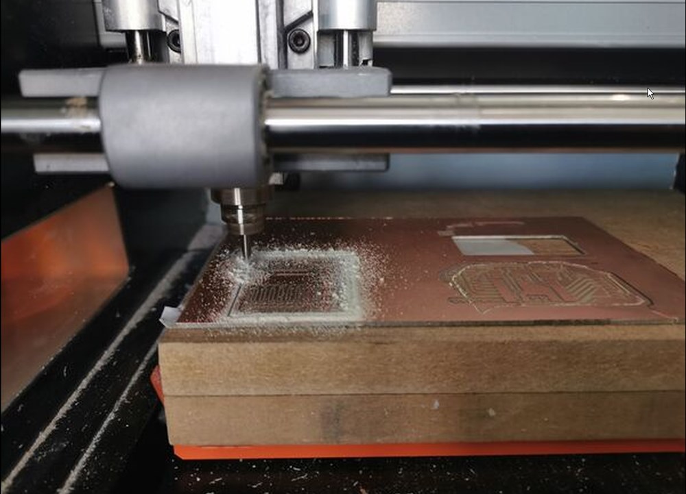
Drilling Holes
Board with drilled holes
Cutout failed
 Second try after cleaning of the plate and double-side tape. Adding more tape and more pressure.
| 1 | 2 |
|---|---|
 |
 |
I realized after making this board that I choose the wrong footprint for the ws2812 leds (2x2mm instead of 5x5mm).
I fixed the PCB design and mill another board.
| 1 | 2 |
|---|---|
 |
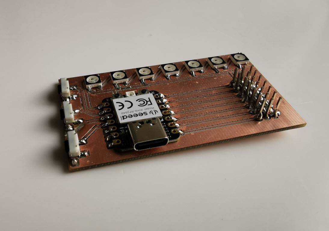 |
Testing the board
It works partialy, leds change color according to current servo angle but some servo doesn’t move as expected, I have to investigate on this later…
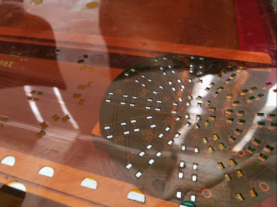
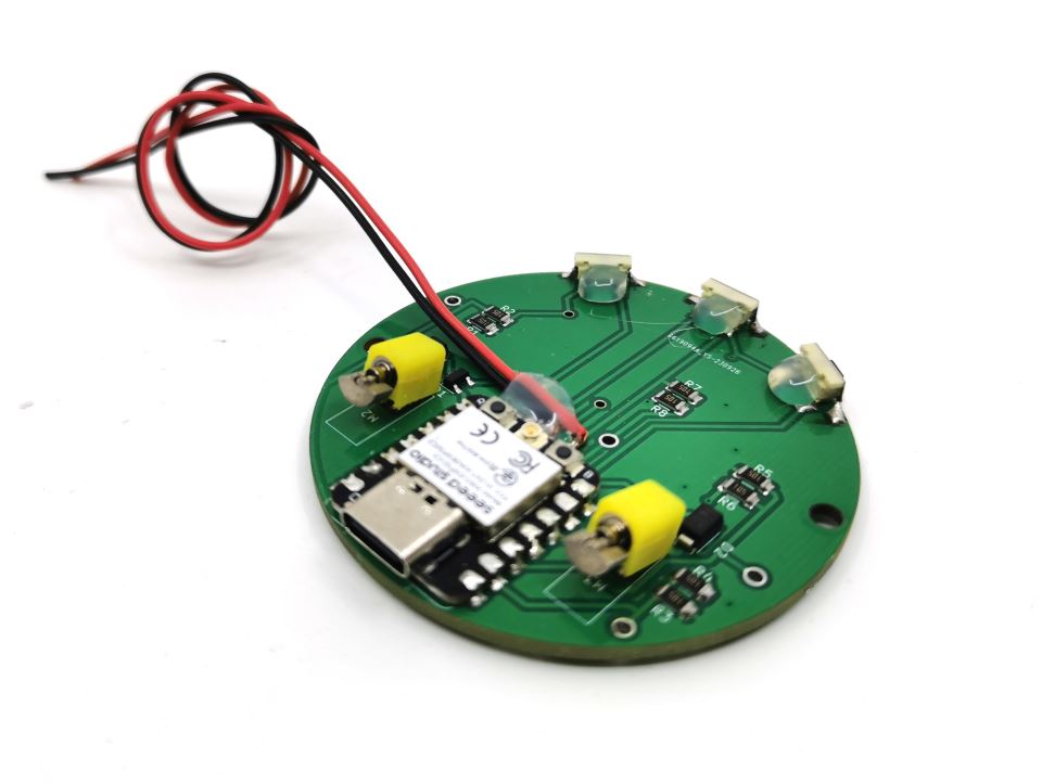
Final Project PCB
I design my final project pcb and mill it on our SRM-20 CNC. But in the same time, I received my board from JLCPCB. I will preferencialy use them as it will be easier to solder my components thank’s to varnish wich leave only the component pads exposed. Furthermore, trace sizes and spacing are quite small to be easily made with CNC method and it require a lot of time for fine tuning both PCB designing and milling. Last point is that the CNC process is can be quite long with so much traces and I wanted several identical boards to make some inter-boards communication tests and final project variations.
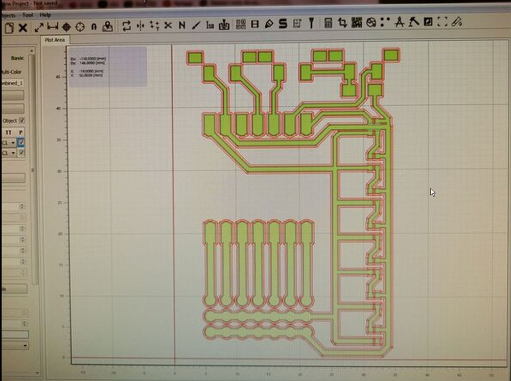
Isolation routing
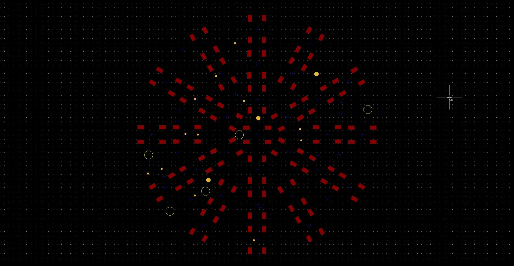
First we load our grbl file, then double-click on it on the left explorer list. Into Isolation routing, put the right Tool diameter according to the choosen bit. Put the number of passes, I let it on 1 to increase overall speed, but a bigger value like 3 can help in easier soldering. Now click on Generate Geometry, we can see in Red line the path generated. I put another example with 3 passes for comparaison.
| 1 | 2 | 3 |
|---|---|---|
 |
 |
 |
Generating CNC Job
Double click on the previously generated geometry on the left explorer list. I choose -0.1mm as milling depth (cut Z). The click on Generate button. We can now see the milling path in Blue.
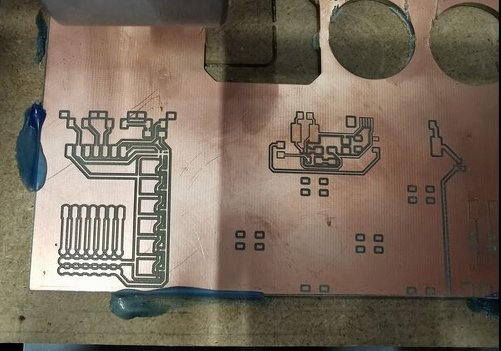
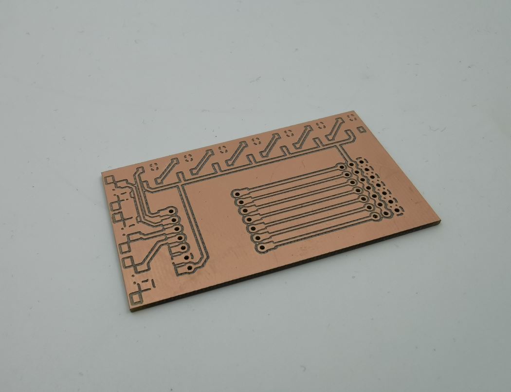
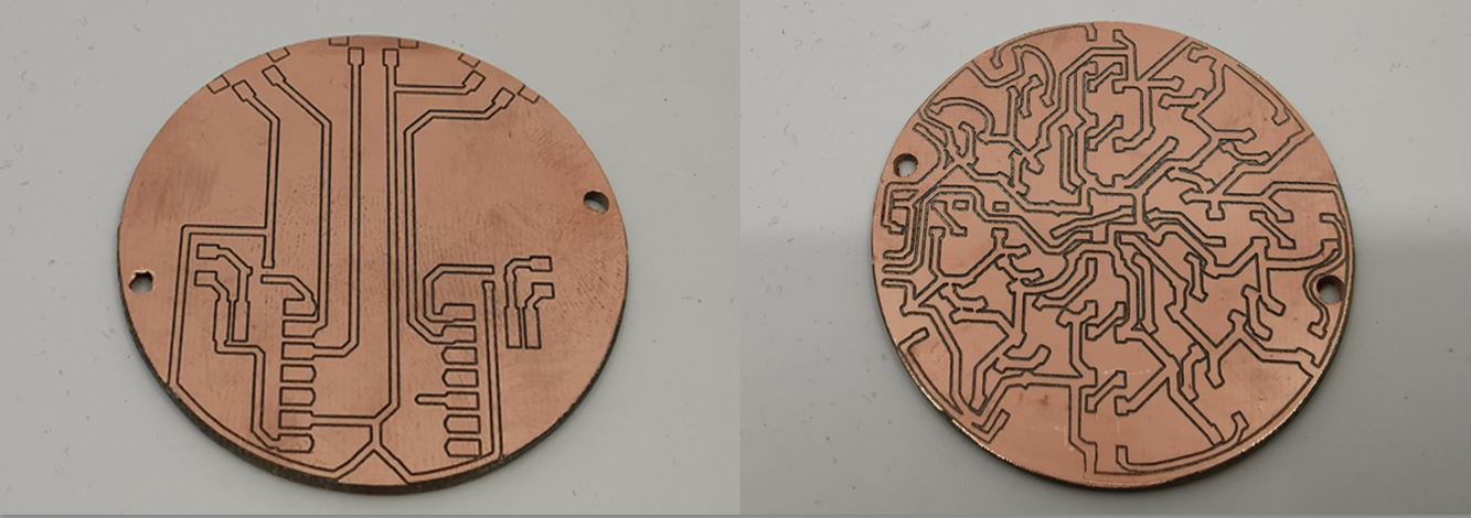
Milling Result
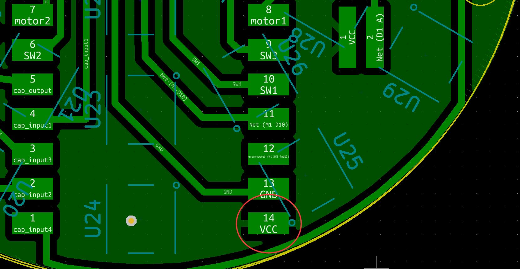
We can see that the milling should have be tune more finely (changing traces width or bit size), there was some pads and tracks are connecting with others. I fixed this with the help of a sharp blade.
Soldering PCB
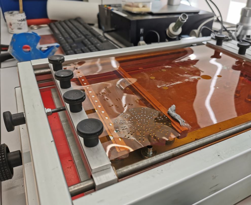
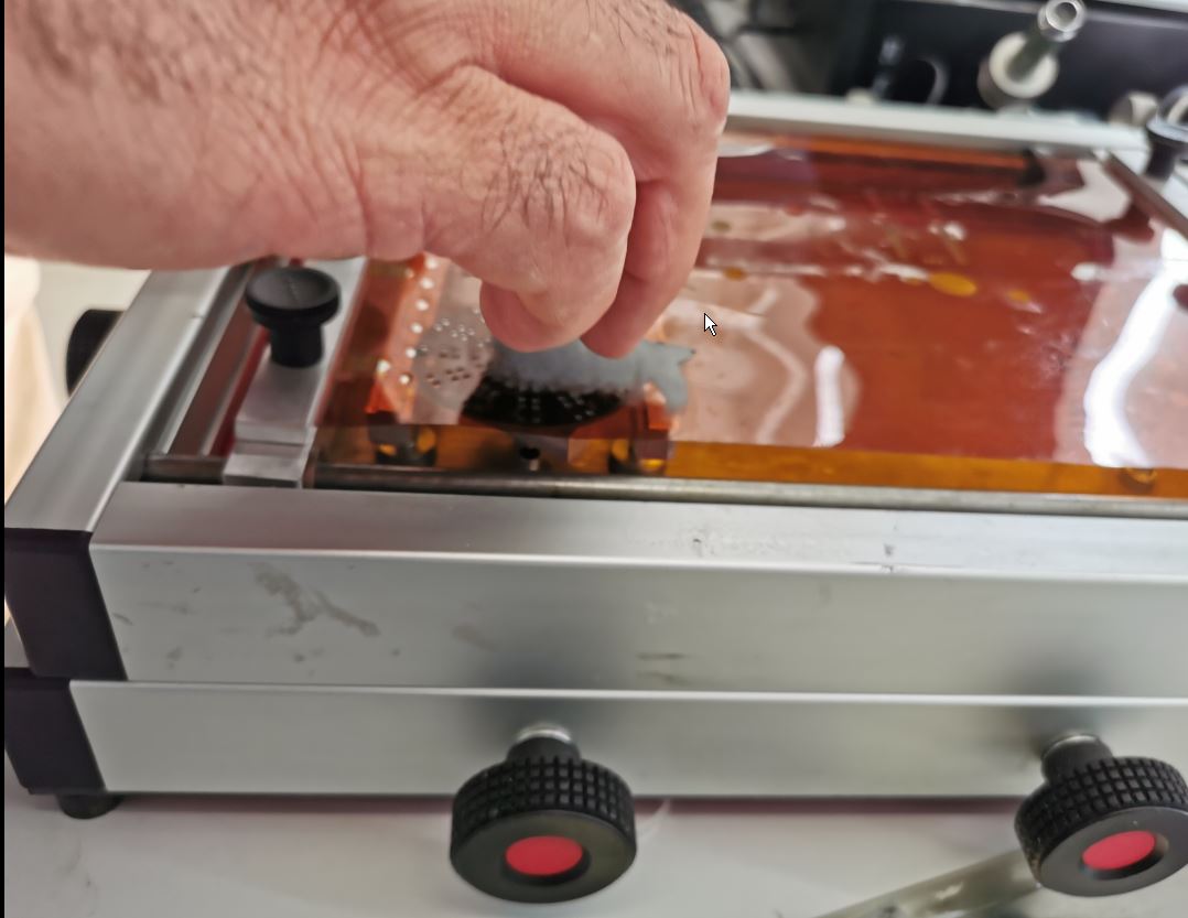
Stencil
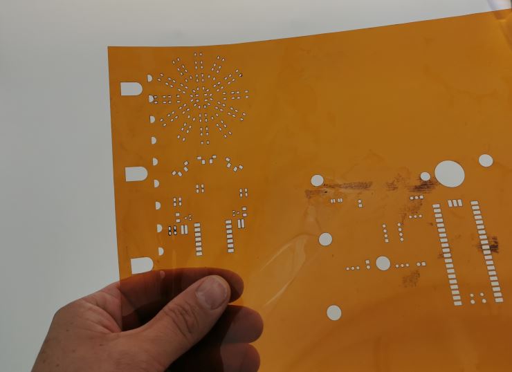
I will use solderpaste to solder my components. I will create a stencil thank to Mylar sheet (REF) and our laser cutter. First I export “F Paste” and “B Paste layer” from KiCad, then I export it into svg format.
I open it in corelDraw, select all the component, modify their properties to have a “hairline” outline and empty infill.
Here is the result after cutting:
I align the stencil with the PCB
I put a little bit of solder past on on end and use a ruler to fill all the pads
| 1 | 2 |
|---|---|
 |
 |
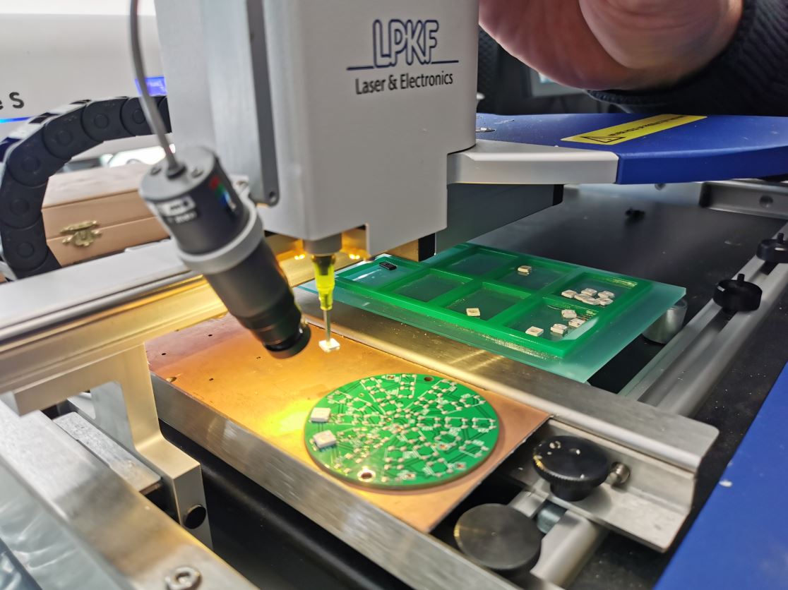
Board population
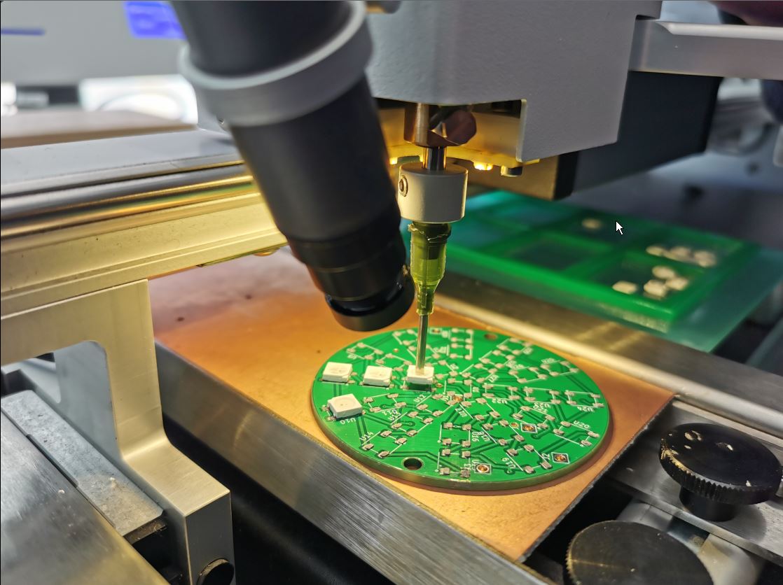
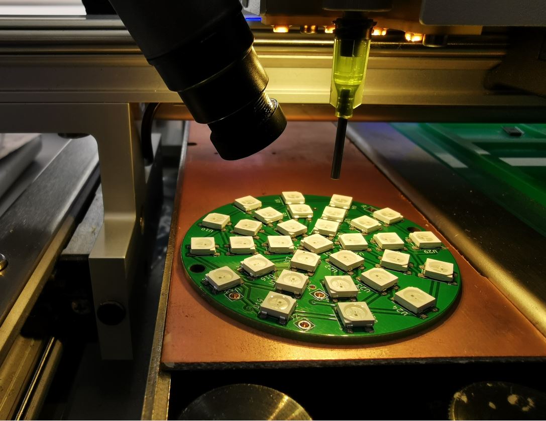
I use a manual pick&place machine to place the components
| 1 | 2 |
|---|---|
 |
 |
A small timelapse of the process:
| Recto | Verso |
|---|---|
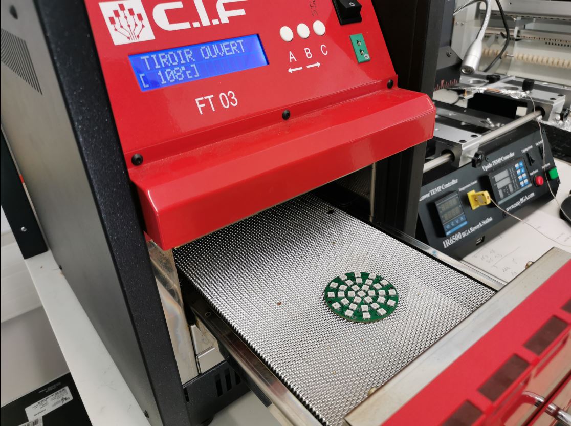
Few minutes later:
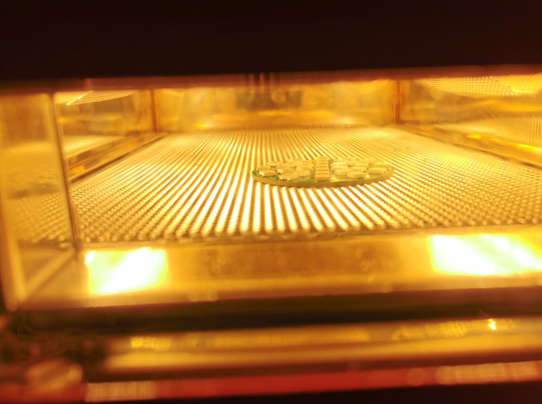
And now, 3 minutes into the oven:
| 1 | 2 |
|---|---|
 |
 |
Oups
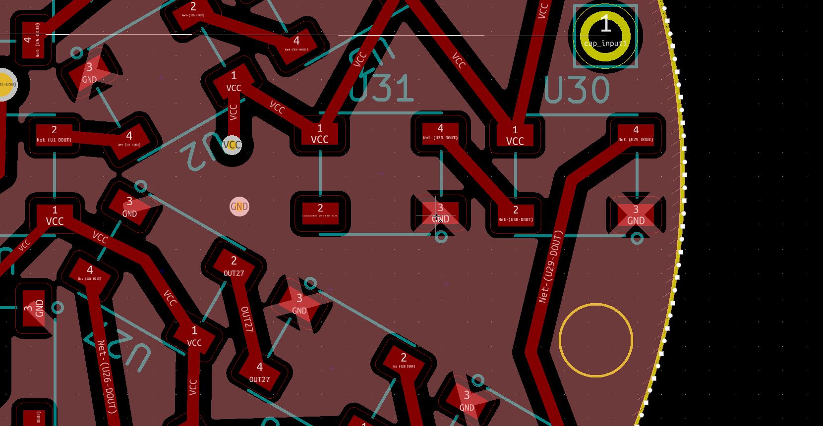
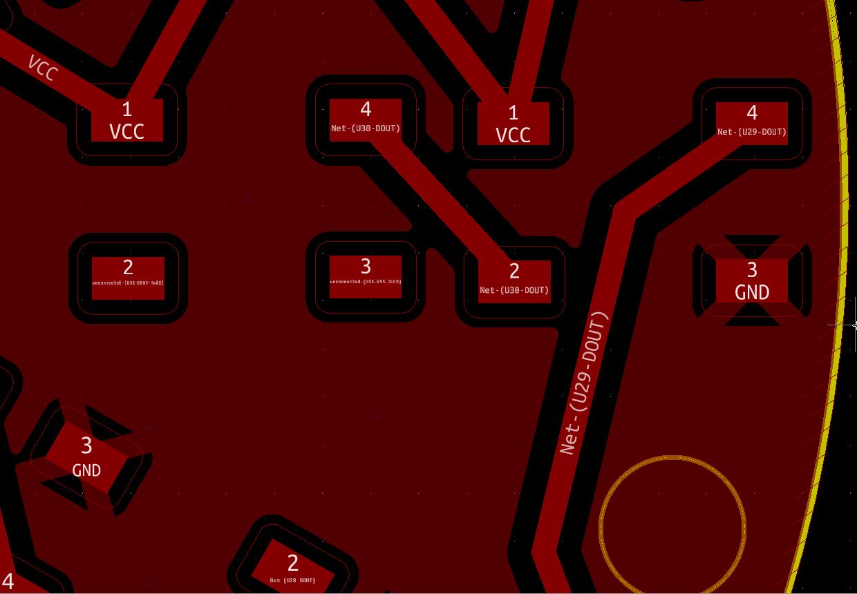
I forgot to route the ground on LED31, I will have to connect it manually.
| Schematic | PCB |
|---|---|
 |
 |
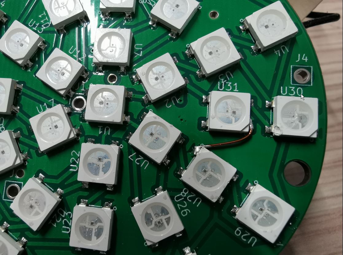
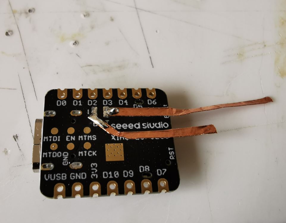
I forgot to make a pad for the batterie too… I create a little “patch” to retrieve the lipo batery input from the back of the esp32-c3 with copper tape.
I apply solder paste to the second face but solder it manually. I add some hot glue to motors, battery wires and switches to reinforce them.
After uploading a test program for the ws2812 leds (FastLed library “DemoReel100” example) and seting the good output pin, it works!
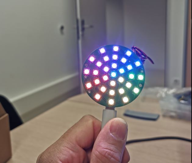
And the vibration motors run at full speed! I should have put pulldown resistors to the mosfets gates.
I setup the middle switch to change the demo mode of the ws2812 example. I setup left and right buttons to switch on the left and right vibrators.
Oups 2
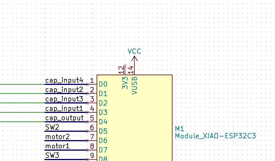
I was wondering why my board doesn’t work’s on batery as well as USB. I realized I made a mistake connecting vcc of my leds and motors to VUSB instead of 3.3V pad of the board.
| wrong setup | correct setup |
|---|---|
 |
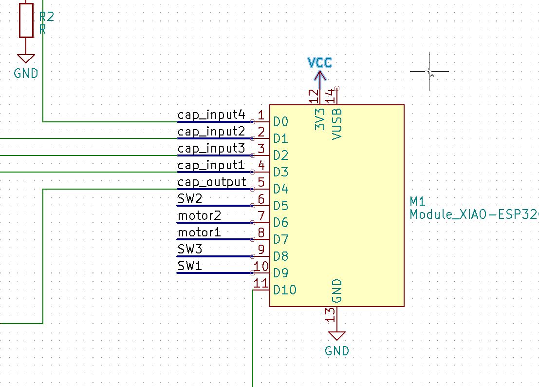 |
Of course the pcb is not good, so I disconnect the VCC copper filling from VUSB to connect it to 3.3V.
| wrong setup | correct setup |
|---|---|
 |
 |