Assessments book for this week:
Slides:
http://academy.cba.mit.edu/classes/electronics_design/index.html (video, review)
Group assignment:
- Use the test equipment in your lab to observe the operation of a microcontroller circuit board (as a minimum, you should demonstrate the use of a multimeter and oscilloscope)
- Document your work on the group work page and reflect what you learned on your individual page
Individual assignment:
- Design a development board to interact and communicate with an embedded microcontroller
Files
Kicad project files: files
This week, I will prepare a PCB for the servomotor controller programmed for the embedding programming week.
It will consist of :
- 1 Xiao RP2040 module
- ws2812b leds
- 7x3 male pinheader
- 3 switches to launch sequences
I will use Kicad for my electronics assigments.
I add 3 row of 7 pin male pinheader that I will arrange in the board editor.
Create a new library
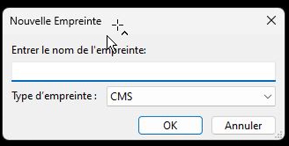
Create a new component
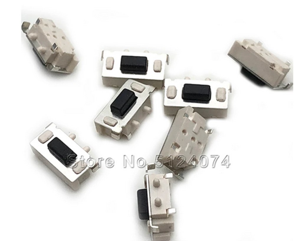
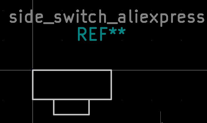
I ordered side smd switches from aliexpress. As there is no name and datasheet available, I will create it for my own measurement.
Footprint
Under Footprint editor go to File> new footprint
Choose a name for that footprint.
First, select Silkscreen as active layer

The differents layers descibing a PCB are called “Stackup”. Most used stackup layers are listed bellow:
- Top and bottom silkscreen layers: This is the visible layer on the top of the board. It contains drawing of components outline, reference sor text. It will not be usefull for our cnc milled pcb but are printed on top of the board when your make your pcb by an online supplier.
- Top and bottom layers: This layer contains traces, pads for surface-mounted components and copper zones. Note that to display text on our cnc milled pcb, we will put it on this layer.
- Top and bottom solder mask layers: This mask can be created with a laser cutter and help to dipense solder past on specific locations (pads of components)
- Edge cuts: outlines of the board. We can put here internal cuts too.
- Drill layer: This layer defines the locations and sizes of the holes needed for through-hole components.
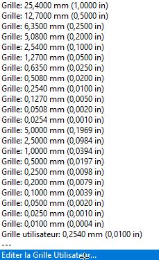
With line tool, draw the outline of the switch. We can left click and set dimension after drawing to adjust with precision. We can also use the grid to snap on predifined position. To adjust the grid, expand the grid dropdown list and “edit user grid”, then select this user defined grid dimension.
| 1 | 2 |
|---|---|
 |
 |
Creating the schematic
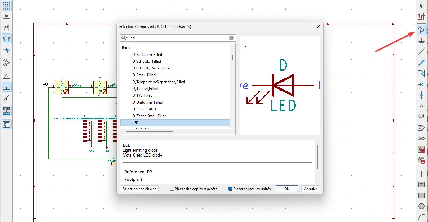
We add components clicking on “Add a symbol” button. We can use the search field to find a specific schematic.
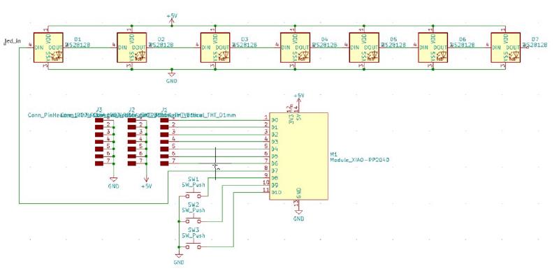
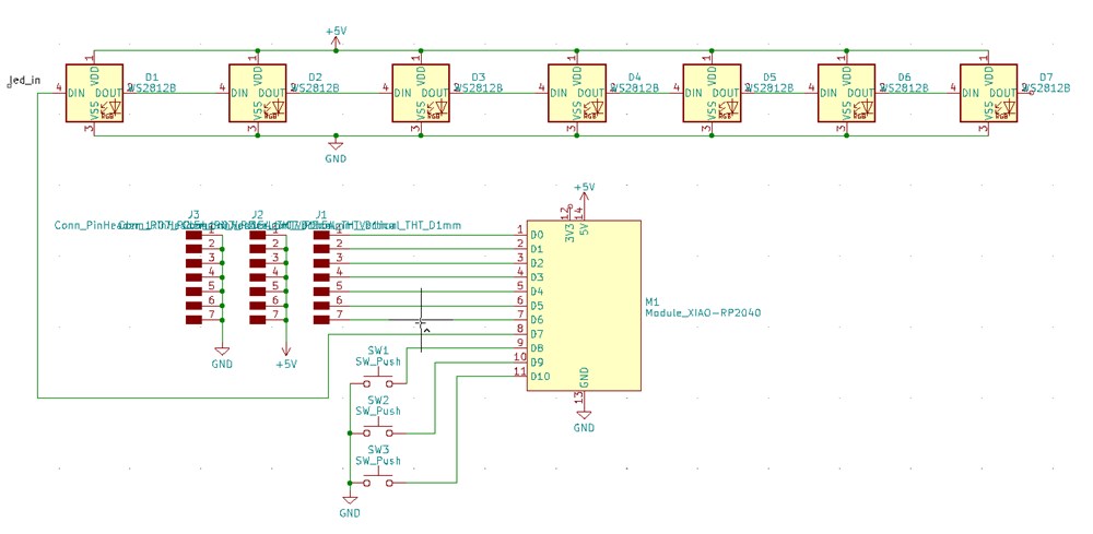
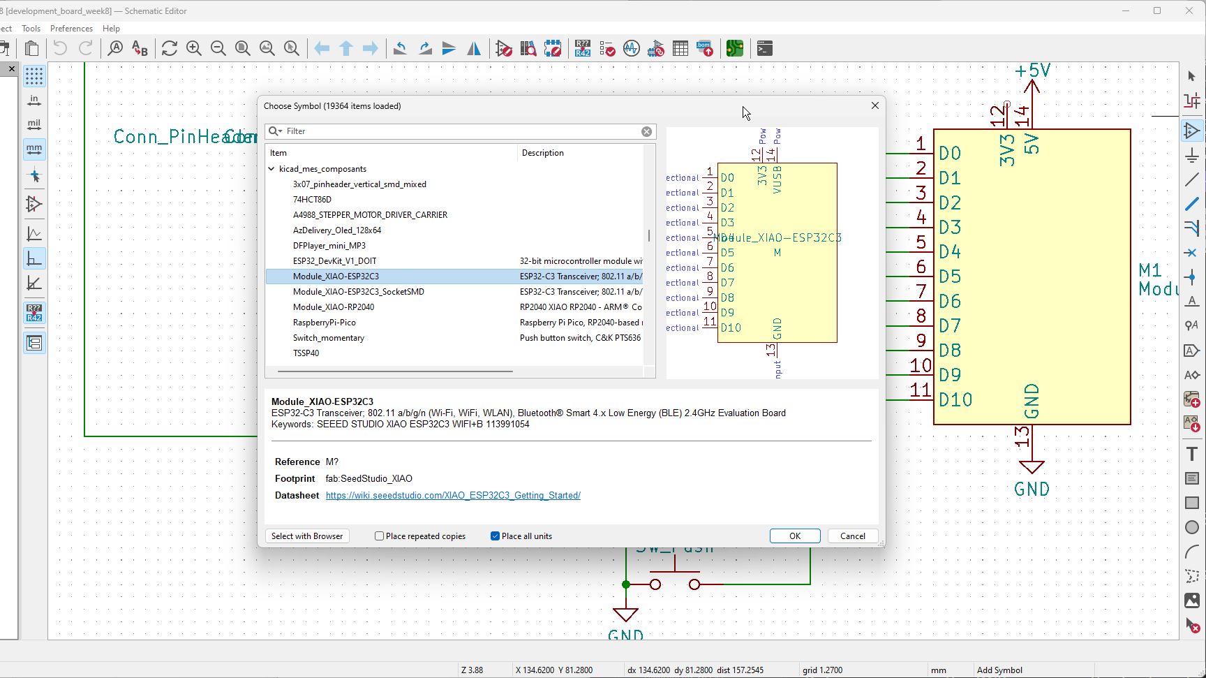
First I add the RP2040 MCU.
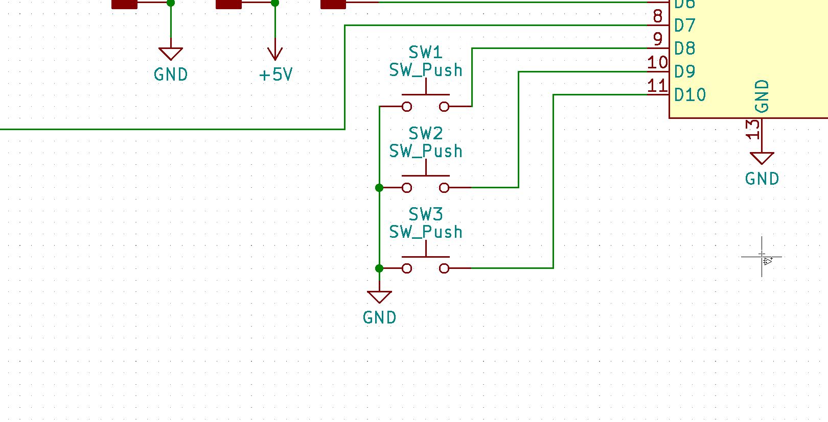
Then I add 3 push buttons for user interface. I connect one side of them to ground (add component > power > Gnd) and the other sides to D8, D9 and D10 pins of the RP2040. On the software side, we will configure those pins as INPUT_PULLUP. Doing this, they are internaly connected to a pullup resistor, setting their value to VCC (HIGH value with digitalRead) by default. When user push a button, it connect the pin to ground and the input value is 0V (LOW value).
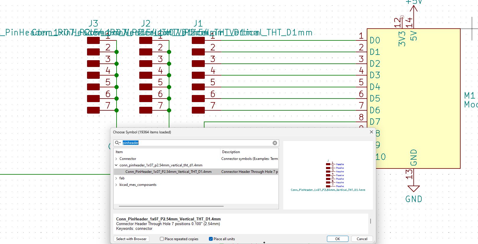
Now I add some pinHeader to connect servomotor. For each servomotor we need 3 pinheaders for ground/vcc/signal. I add 3 set of 1x7 male pinheader (conn_pinheader_1x07_p2.54mm_vertical_tht_d1.4mm). One set is connected to ground, the other to Vcc. For the last one, I connect each pin to a separate input of the MCU. Connection is done using “Add a wire” button.
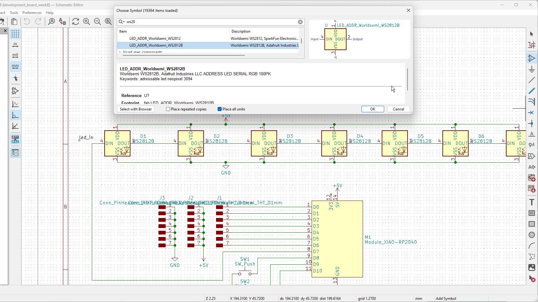
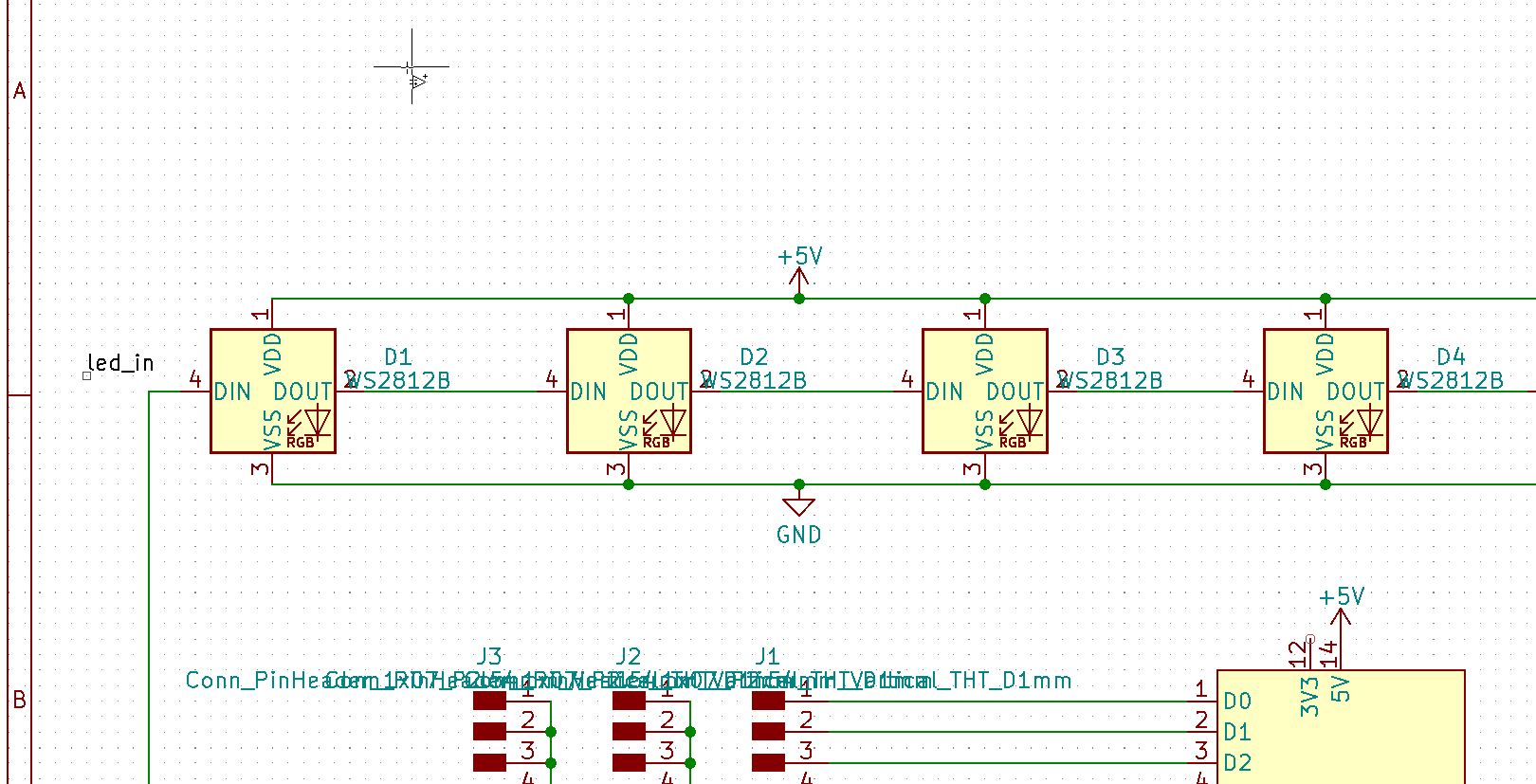
Finally, I add 7 ws2812b leds. Those leds can be chained connecting Dout of led0 to Din of led1, then Dout of led1 to Din of led2, etc… I connect all led’s VCC to +5V (add component > power >+5V) and all led’s ground to GND. The first Din is connected to D7 of the RP2040 and all other leds are chained together.
| 1 | 2 |
|---|---|
 |
 |
PCB design
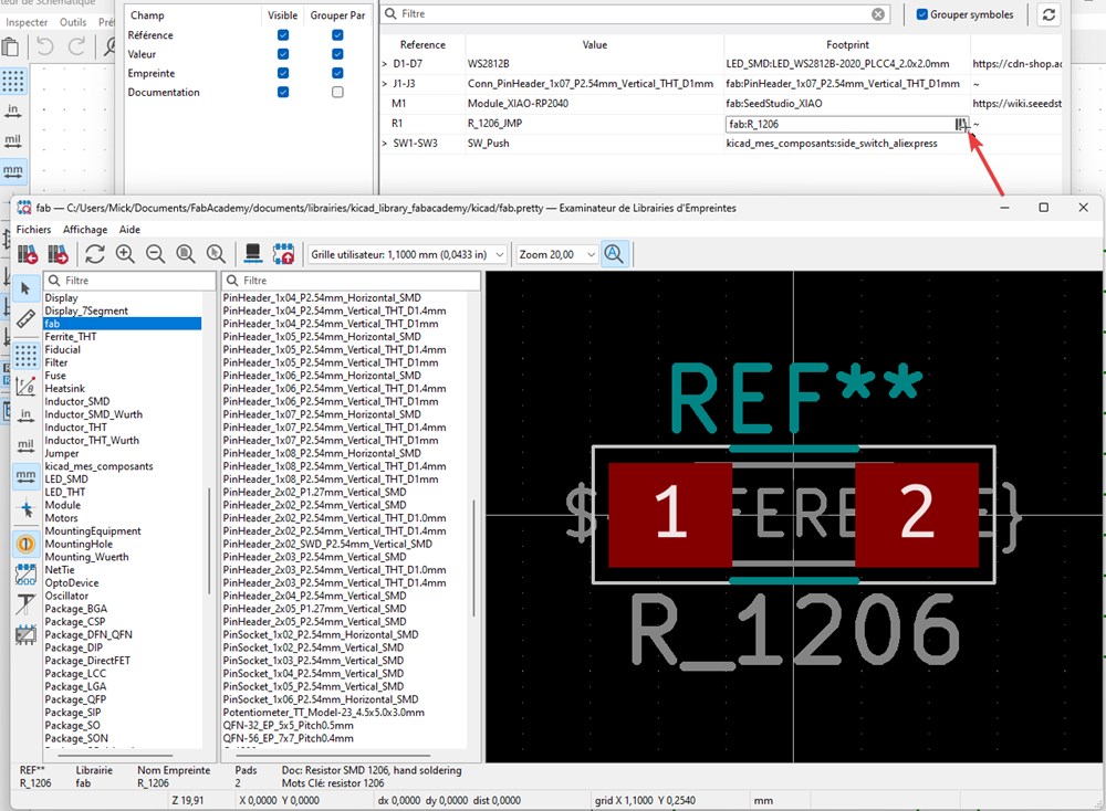
In Kicad, footprints and schematics are distincts entities, it allow for example to have the same symbol for a resistor and match it with a through hole resistor, 1206 (1,2x0,6mm) SMD resistor, 0805 (0,8x0,6mm) resistor etc… The constrain to match a symbol and a footprint is to have the same number and naming of pads on both side.
Before preparing the PCB, we open the footprint-schematic lookup table.
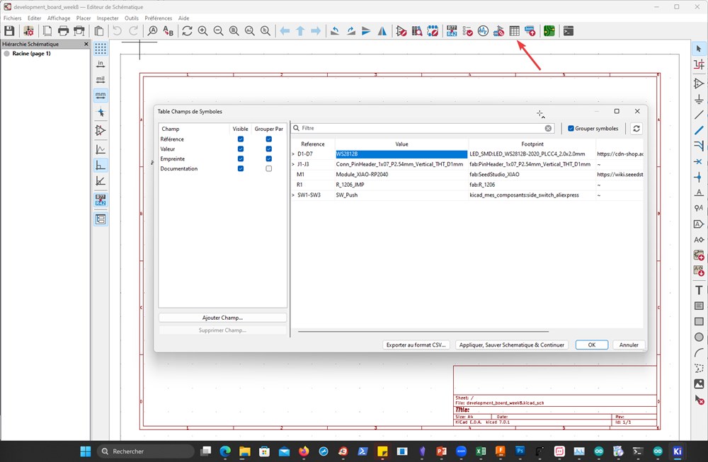
Click on the icon on left of the footprint line.
It open a window with all loaded footprints, validate it by double clicking.
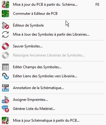
Now go to Tools>Update PCB from schematics then Switch to PCB editor.
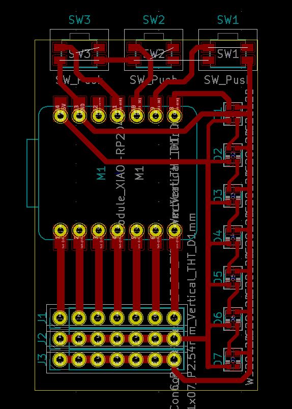
Now that our schematic is done, we place components in relation to each other, optimising this placement to simplify trace paths.
To create the board outline (in yellow bellow), select edge cuts layer and draw the outline with one of the drawing tools (line, rectangle, arc, polygone, circle)
Export files for fabrication
As an image
Cutout and Copper layers
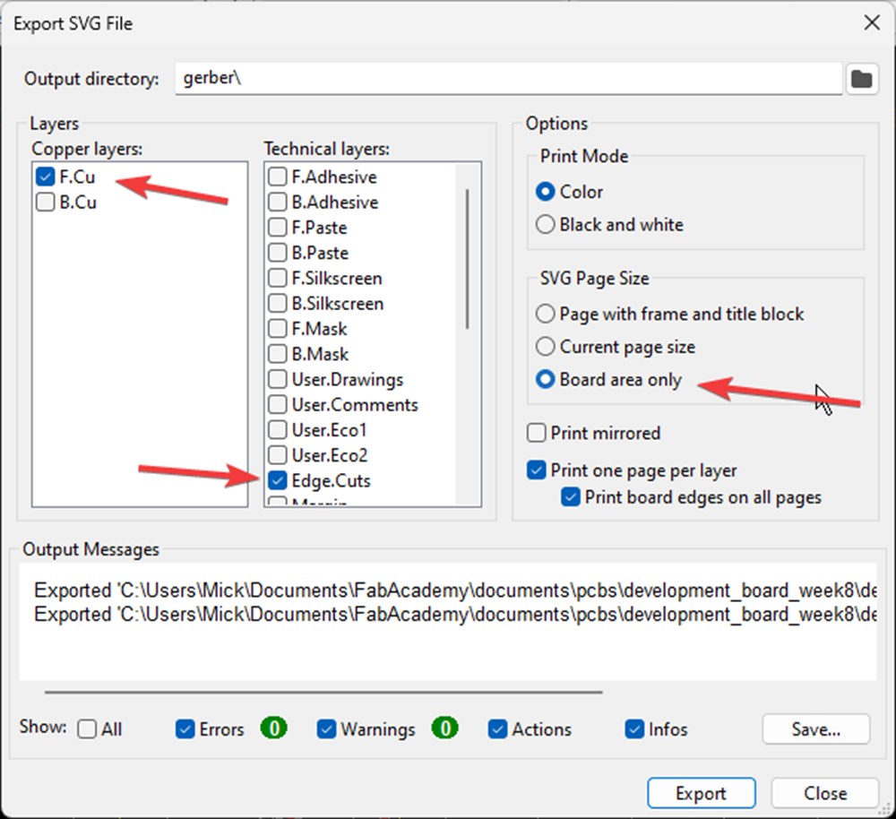
File>export>SVG… For our single side PCB, we can select only F.Cu and Edge.Cuts. Choose “Board Area Only” into SVG Page Size section.
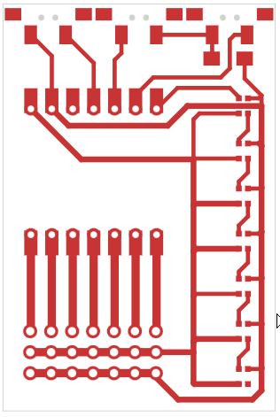
Files: Top copper layer svg Edge cuts scg
As you can see, their is unwanted holes comming from my home made side switch footprint, I have to edit it to add move those holes in the drill layer instead
As Gerber Files
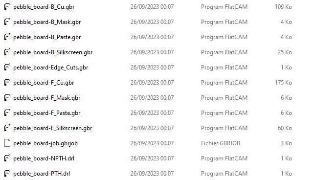
Gerber files describe every layer in the design, usually we package and those files togother into a zip file before sending them to a fabrication fab like JLPCB or PCBNEW. Here, like with image export, we only need 2 layer for our pcb milling.
Copper and cutout
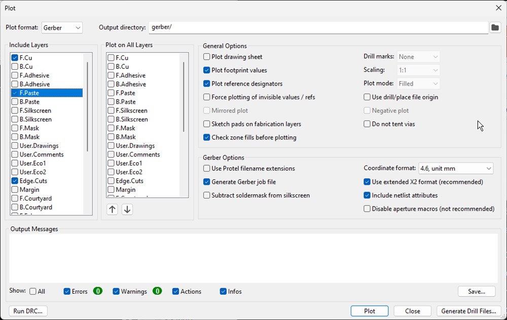
Go to File>Fabrication Outputs> Gerbers and select needed layers, Then click on Plot.
Drill file
For this design, I have some passthrought components. Holes driling is described into another kind of file.
Go to File>Fabrication outputs>Drill Files. Then Generate Drill File or, into the previous Gerber export windows, simply click on “Generate Drill Files” button.