
The task list for this week:
- Group assignment:
- Use the test equipment in your lab to observe the operation of a microcontroller circuit board (in minimum, check operating voltage on the board with multimeter or voltmeter and use an oscilloscope to check noise of operating voltage and interpret a data signal)
- Document your work to the group work page and reflect on your individual page what you learned
- Individual assignments.
- Redraw one of the echo hello-world boards or something equivalent.
- Add (at least) a button and LED (with current-limiting resistor) or equivalent input and output
- Check the design rules
- Make it and test it
- Optionally, simulate its operation.
Group assignment:
Testing equipment in our lab:
This assignment was about documenting what we learned about test equipment in our lab to observe the operation of one of the eco Hello Word bord we designed this week. Where we check operating voltage, Digital signals, and power consumption, on one of the boards in our lab. We also check the noise of operating voltage and interpret a data signal of blinking led on the Board.
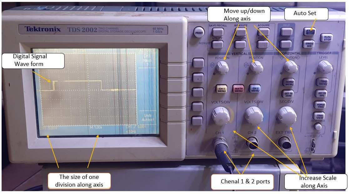
Digital signal of blinking led on DOS.
We have 3 major electrical testing equipment in our lab for testing electrical devices which include an RPS-3005 DC Regulated Power Supply , a digital multimeter, and a Digital Signal Oscilloscope.
Check here to read more about our group assigment.
Individual assignments:
Making a Hello World Board:
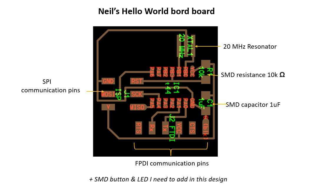
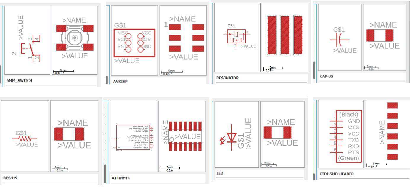
For our individual assignment this week we need to redraw one of the echo hello-world boards,based on the ATtiny44 blink ATtiny44 blink board and add a button and a LED (with current-limiting resistor) . For reference I fallow this schematic bord and aditionaly added a smd LED and an push butten to it to recreat my hallow word bord designe.
.
Eagle:
For design my costum eco hello world bord PCB I use Egle program . EAGLE is electronic design automation (EDA) software that lets printed circuit board (PCB) designers seamlessly connect schematic diagrams, component placement, PCB routing and comprehensive library content.our instructor suhas Introduce us with the software. And i found it relevant to design PCB in it .It was my first time designing an PCB.

.
Download and Install Eagle:
Fab Academy provides me with a student licence for Egle software I install and download my Egle software from there. but one can get the student licence by visiting the Autodesk official website.
Get Eagle here I fallow this guid line to "how to install the Egle " which help me a lot.Creating new project
PCB design in EAGLE is a two-step process. First, you design your schematic, then you lay out a PCB based on that schematic.
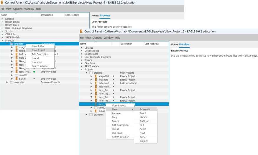
To start with the eagle. I start by making a new project folder for my design. for that, I fall these steps.
Eagle control panel>Projects tree> user project>new folder>New >Schametic.
Clicking on Scametic a new window will pop up.
Project folders in Eagle are like any regular file folder system, having a file name ending with "eagle. epf".
.
Eagle Schametic.
As I say by clicking on Scametic window I was on Scametic page.The project folder will house both our schematic and board design files. To begin the design process, we need to lay out a schematic. To add a schematic to a project folder, right-click the folder, hover over "New" and select "Schematic".as shown in privious image.
What is Schametic?
A Scametic is a representation of symbolic electronic circuit digram.we use it to make circuit design more simpler and understandable .In PCB designing similar like CAD design drawing sheet Scametic is a symbolic representation of real world electronic compone which are connected by lines which are called traces to show the connection between each electronic component in circuit.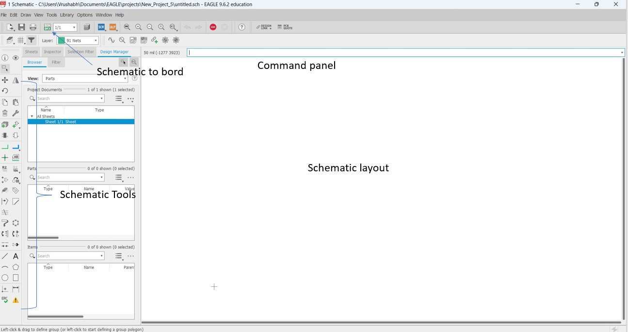
.
This is a very use full link . "how to read a scametic " where I learn how to read a scametic Symbol.
Installing libery
For adding the Scammetic component I need a Eagle component librari .Eagle has a lot of built in libraries of components in its default liberaries .one can also import component liberiory for 3rd party resources for there project.The fab network also maintains a library.where one can get all the components require for making this hello world bord.Here is how I install the libraries.
Step 1:Go to
FabAcademany-Resources
git hub account.
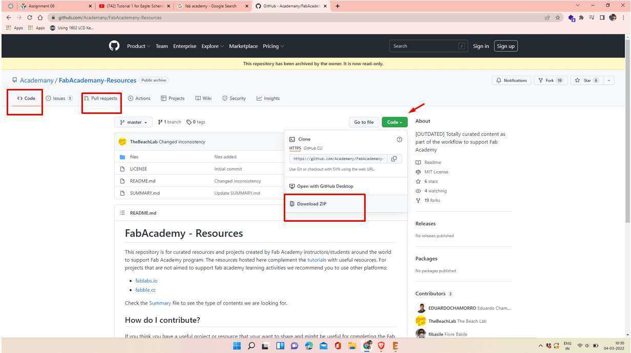
Step 2:Open the schematic windo of Eagle .Go to Tool bar >Library>Library Manager>Avalabe Then I open the Fab library in It and and click on Use button.
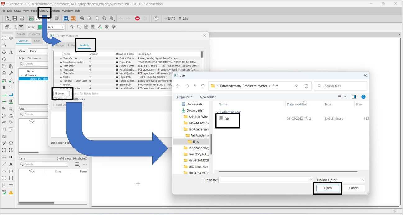
.
Step 3: Now I switch in to Use section and Search for Fab .I got it that mins the library is added sussfuly.
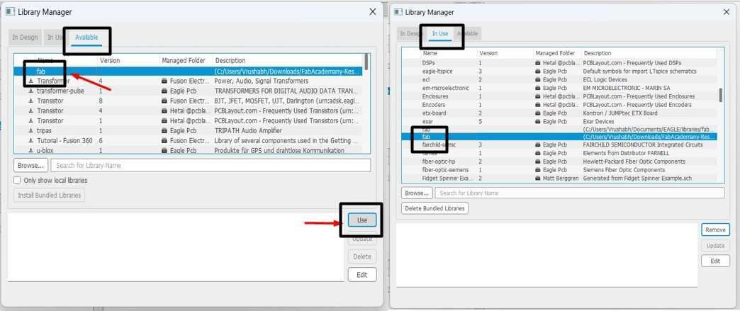
.
Add Tool.
The ADD Tool (on the left toolbar, or under the Edit menu) -- is what I use to place every single component on the schematic. The ADD tool opens up a library navigator, where I expand Fab libraries and look at the parts it holds. With a part selected on the left side, the view on the right half should update to show both the schematic symbol of the part and its package. One can also use Eagle terminal command Add to call the Add tool.
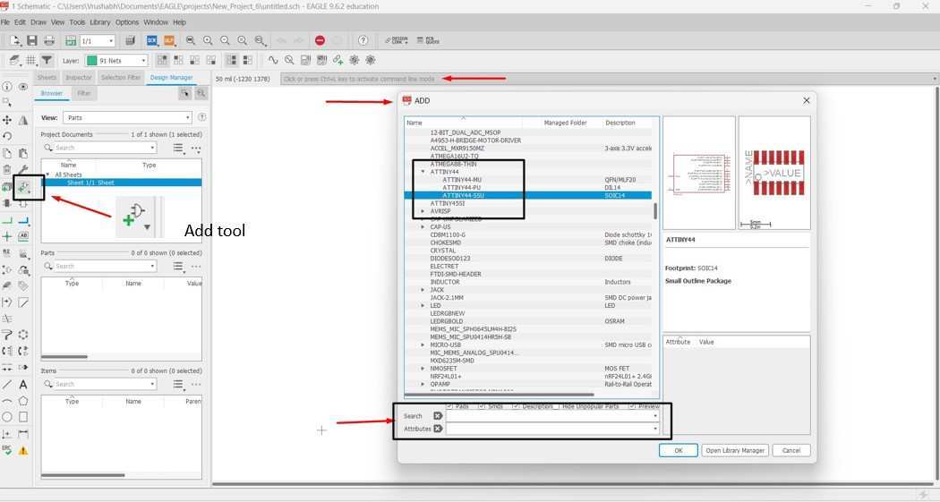
.
The Add Tool also have its search function at bottom .But I found it difficult to us .It shows some time issues of missing Liberies If I open once aggen.To solve this essue I copy pest the liberty folder in Document>Eagle>Libary to make it add in permently. For searching a specific package I just Press the First alphabet latter and the Packeg Liberari was listed out on screen.
To actually add a part from a library either select the part you want and click "OK", or double-click your part.The part will automation pop up on schematic window clicking right to pest it.
Adding Parts to a Schematic.
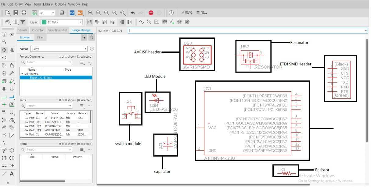
Schematic design is a two step process. First you have to add all of the parts to the schematic sheet, then to connect them together to make a possabil scametic circuit digram. As I am referring to the neil Hello Eco World bord I know what component I needed .So I just add everything in one swoop.
.
.
Wiring Up the Schematic.
Net Tool.
After adding all parts to schematic, it's time to wire them together.for wiring portion I use Net tool (left toolbar, or under the Draw menu).
Instate of wire tool to connect the components togather.
I find NET does a better job of connecting components as com pare to wire tool.
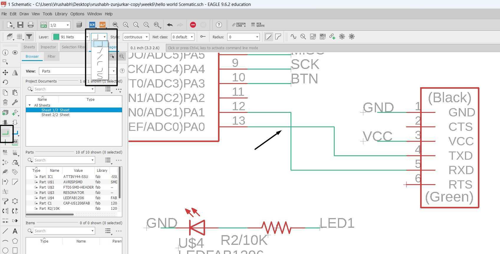
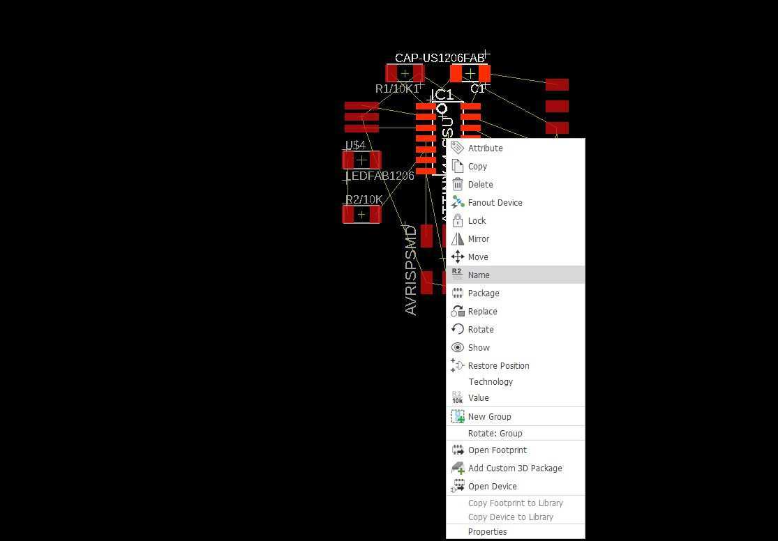
Name Tool, Labeled Net Stubs.
I use Name tool to connect two pins of different components.Its become difficult and to wire hole scametic using net tool all over .So name tool is very help full in such casses .
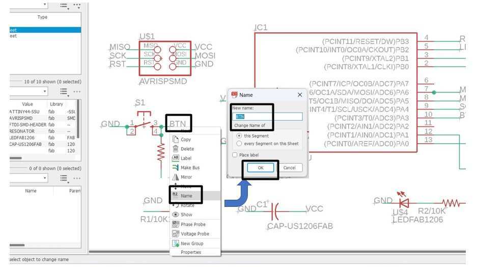
I first
- I use pin 10 (PA3) on the ATtiny44 to connect to the button.
- And pin 5 (PA2) on the ATtiny44 to connect to the LED
Complet wired Scametic design.
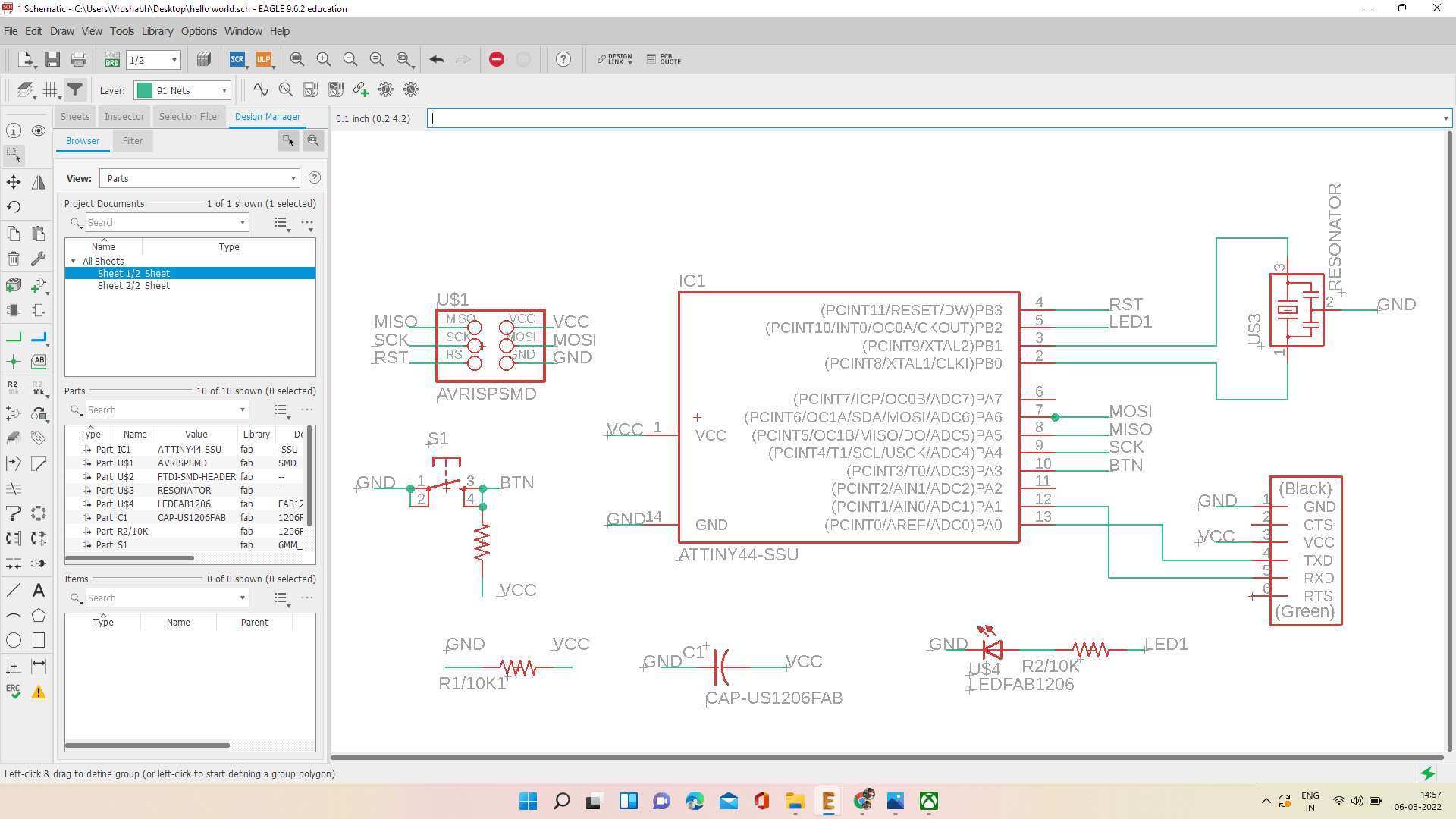
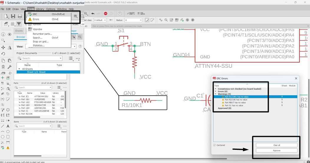
ERC cheking.
ERC stand for Electrical Rules Check (ERC) enables PCB this function cheks the electronic design falts in your Eagle design .such as components connectivity,components value , there nomenclature,tresses overlapping etc.
To chek ERC in Eagle go to :
Toobar>Tool>ERC.
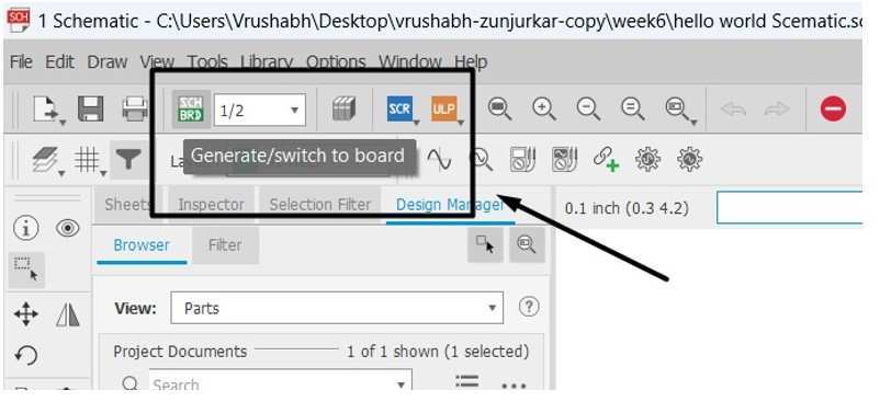
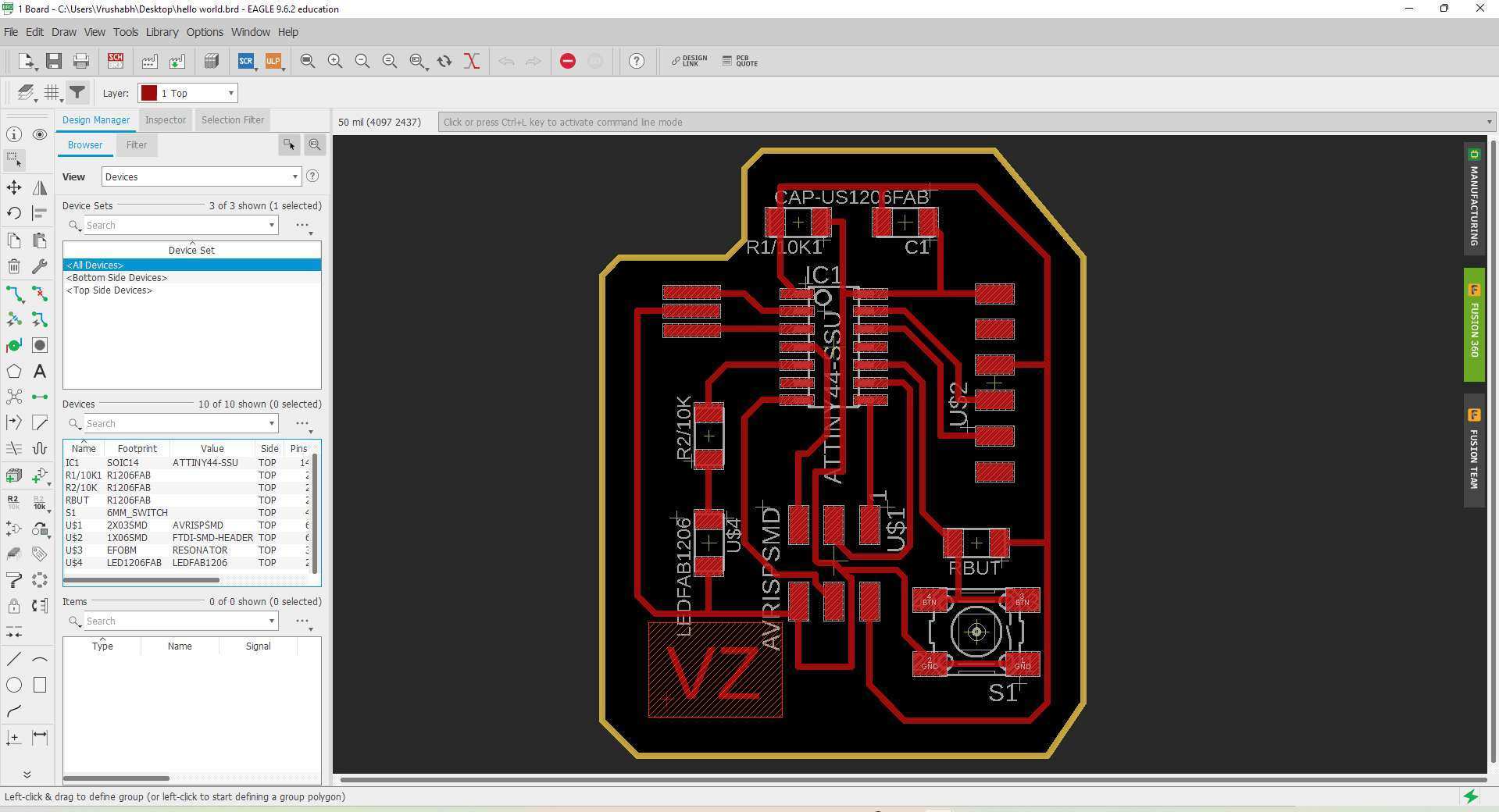
Creating PCB layout
- To switch to the board view I click on the button at the left corner at the top.
-
or I can use another method For that
Go to the top menu > File > switch to board.
.
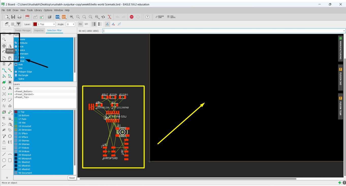
- The components I have just added was jumbled up in a corner with yellow unrouted traces attached.
- Then I drage them all and select them and Use "move" tool to move each individual component around at center .
As soon I switch to the bord view The board view open up.
.
- Key Move: I arrange them in the centre and orient them in such a way that I can easily route them using routing tool .
- For that, I just Right-click on the mouse and a list of tools appear I use the move, rotate, copy etc. to make the above formate.
.
Seting Design rule for bord.
Design Rule Check allows one to establish a set of boundaries for PCB trace widths, component spacing, diameters, etc. It’s only after I have all of these rules set up . that I can then go about completing my design process, knowing that any issue with these manufacturing-specific constraints will be flagged in Autodesk EAGLE when I run my DRC. In my case, I need to check that the endmill I am using (1/64 usually) is able to go between all the traces so the machine is able to cut successfully the board. For that, Design Rules Check is used which will check that there is enough space everywhere.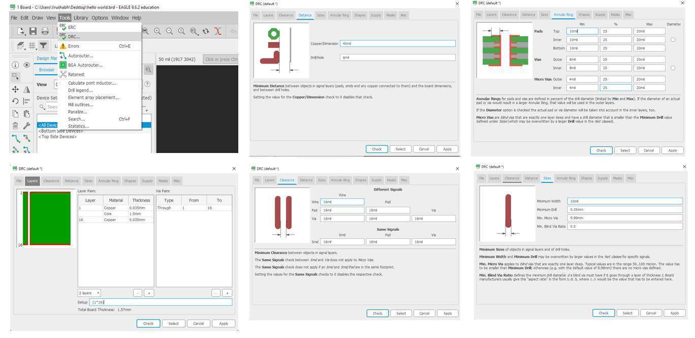
Above are some set of Design rule I set for my design specific.
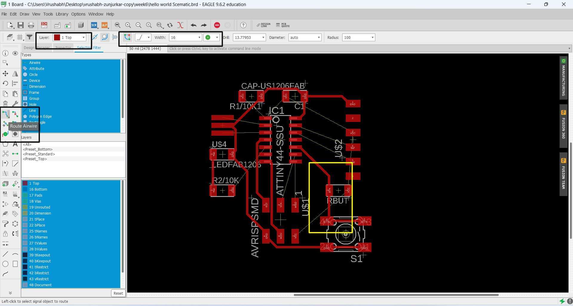
PCB Routing .
I use the "route" Tool to route each trace. The wire gets turn red as I route it into place.
After route wires, I use the "move" tool to move them around as lines.
There is also an autorouter feature - it is good for making a general layout, I try to use it but sometimes if the components were not properly oriented, It some time rout through the bottom or makes the design more complicated. Then after all this, I have to edit the traces manually. Especially on this circuit.
to use the autorouter go to the "tools" menu in the top toolbar and select "auto".one can also call auto tool by just clicking arrow aside rout too on left bar.
Testing Design rule for bord.
For checking DRC .
I go to Toolbar >Tool >DRC>check
A small window with the list of error messages appears at the left bottom corner.
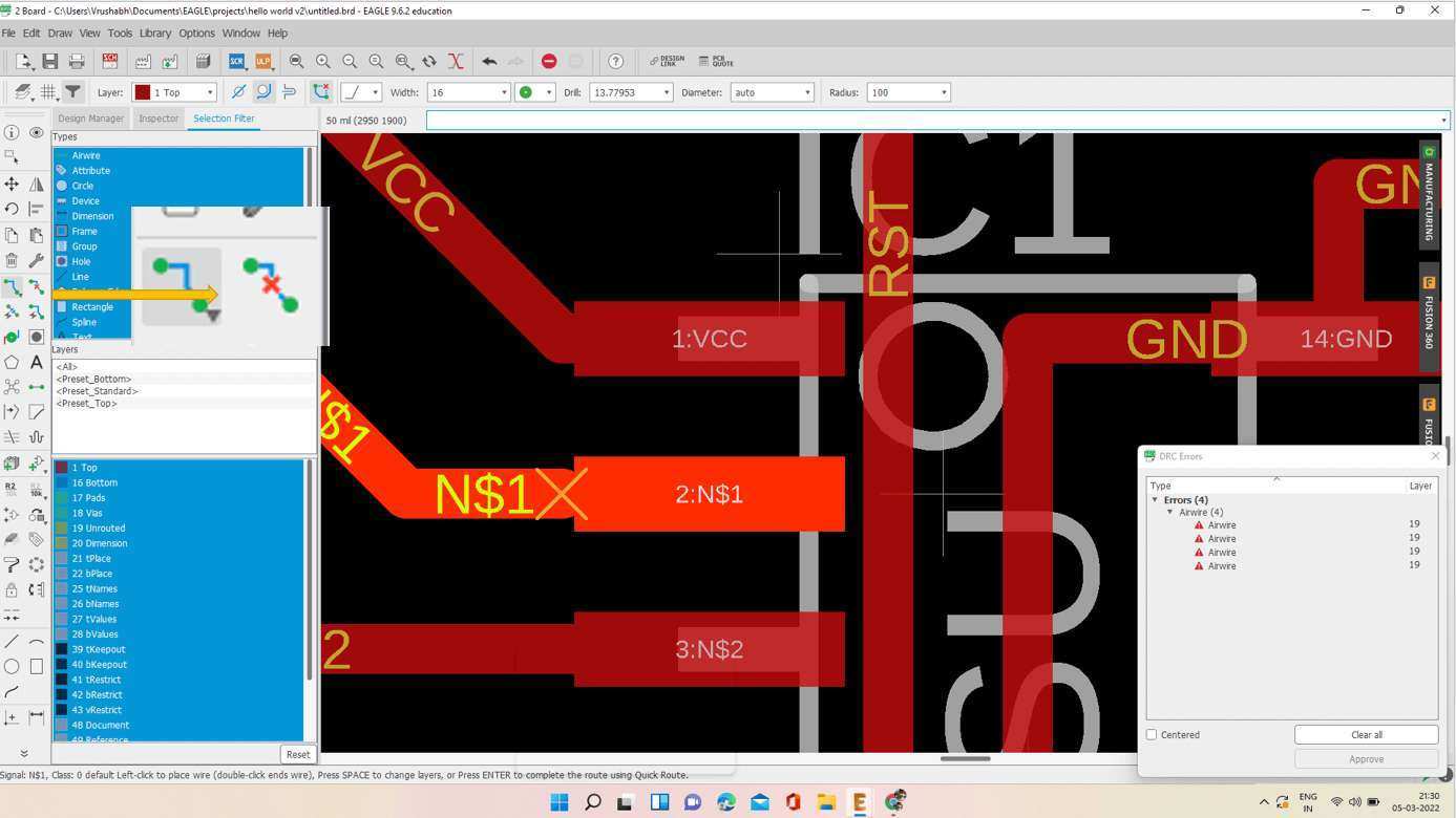
I got some Error messages from Airwire which might mine there is some kind of overlapping or improper connectivity between two tresses. I use the unrout command and re-rot all the routing where it was necessary to solve the error.

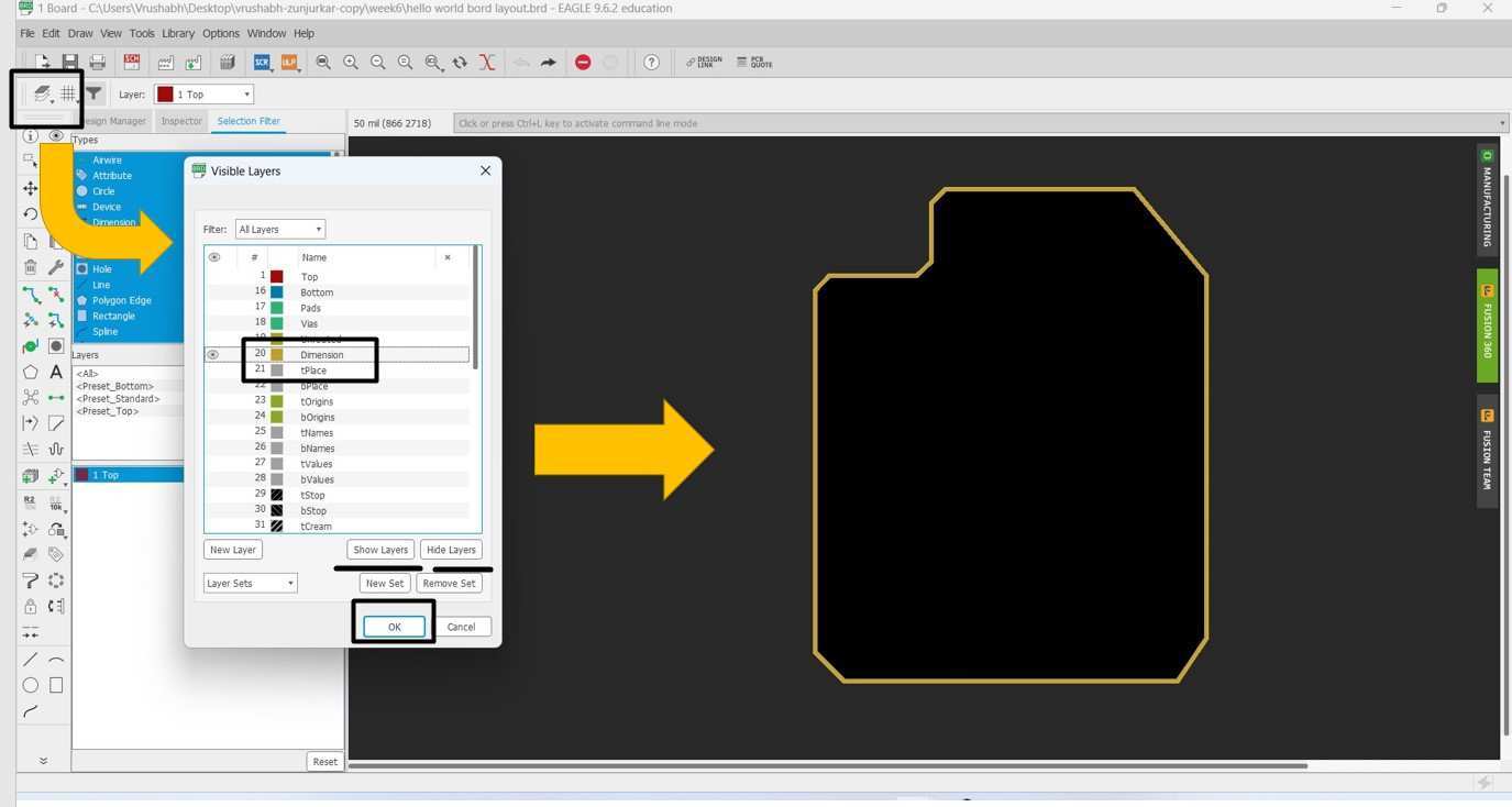
Routing the outcut border.
For making an outcut border for my PCB design. I change the layer colour to yellow (Dimension ) and use the line command to draw the out cut border pattern.
Which you can see in the below image.
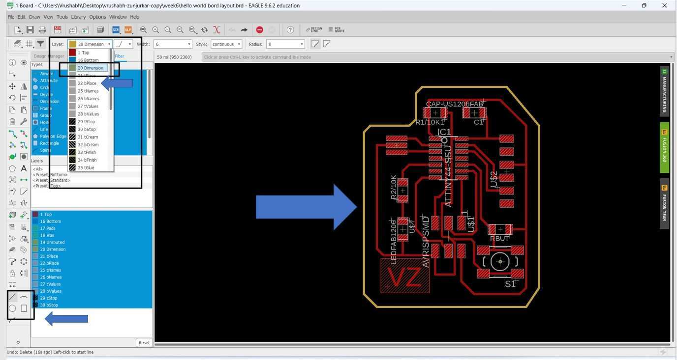
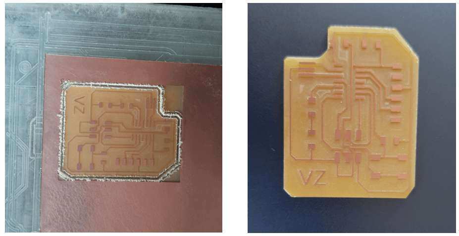
At last I use the Text command to add my signature as an initiative of my name VZ on the board.
And hence the designing portion is completed. you can see my final complete image above.
Exporting a board design.
For milling my PCB in SRM-20 I know I will require a jpg image formate as I did at electronic production one for traces and one for output.
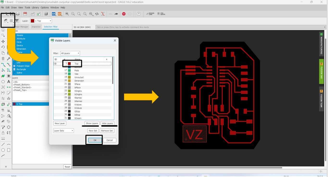
For generating jpg for traces I need to hide all unnecessary layers in the PCB design.
For that, I go to the Layers
menu in the top toolbar and I use the hide button for unseen all the layers and select only the top layer (traces only).
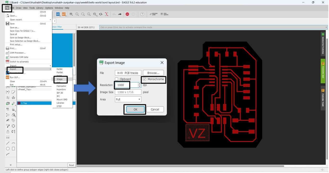
For Exporting Images in jpg formate
I go to the
toolbar>Files>Export>Image.
An Export Image window open.
Then Select the suitable path for saving the Image.
Values that I Modify
- Settings should be MONOCHROME
- Resolution:700 DPI - this will export an image with white traces.
- Area:Full
Similarly, I select then export the Dimension layer for milling the outside of the board and repeat the above stape to generate a jpg image of the outside border.
- Remember: the Modela cuts out the DARK and leaves white at the default setting. you can invert it in modes if you want.
And hence the jpg export portion was completed. These are final Export jpg files of my hello world bord.

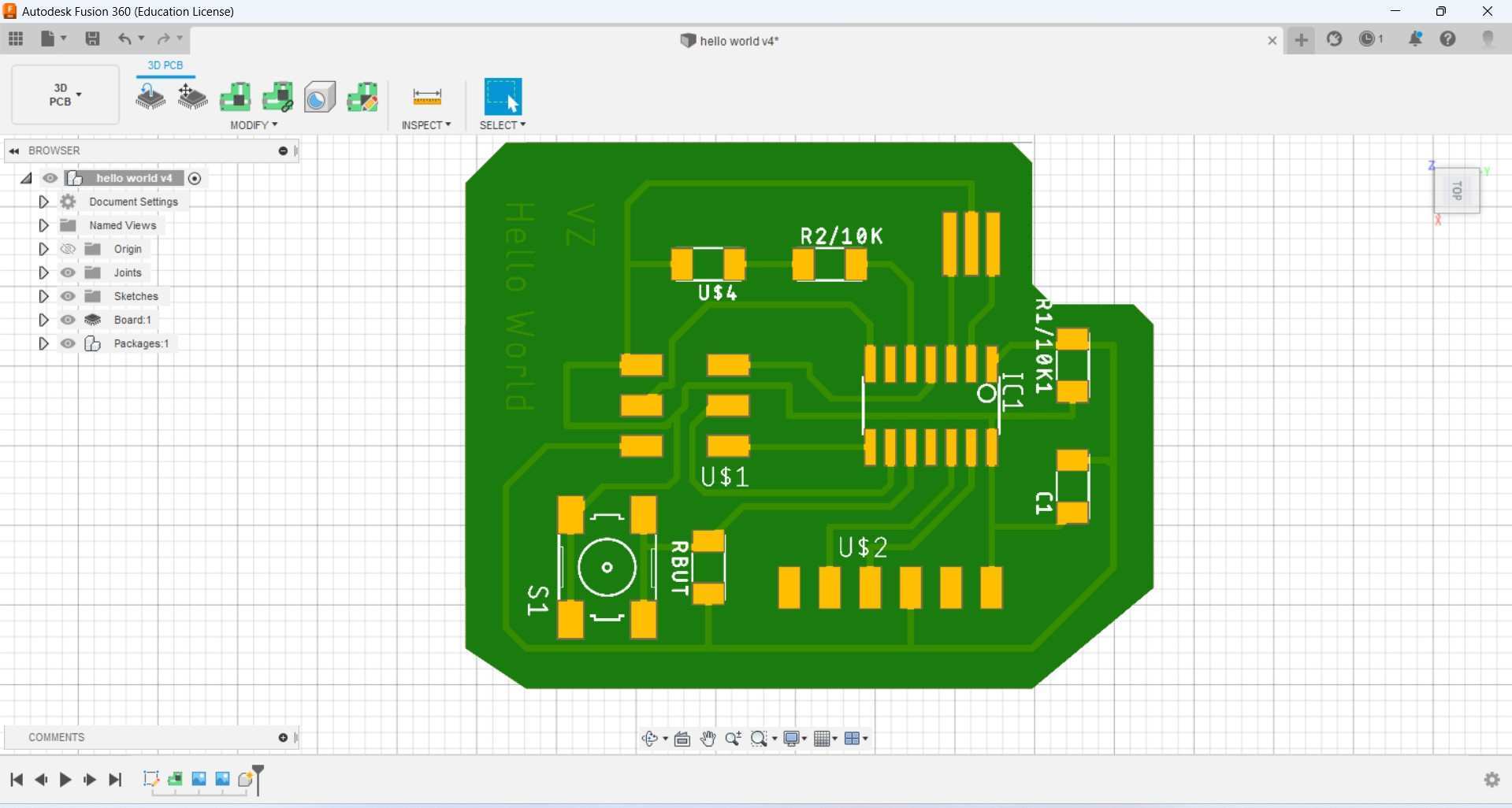
Fusion 360 PCB Designe.
I try to open the PCB design in fusion 360 for that I just click on the extreme right button on eagle where I found the path to connect the fusion software I push the eagle file then on fusion 360 cloud and open it in CAD enveromentr..
Generating Modes rml file.
This portion of generating rml file is already briefly explained by me in the Electronic production week. Please visit the week assignment page if you are interested to read more about it. For this week here I generate the rml file for milling PCB traces on SRM-20.
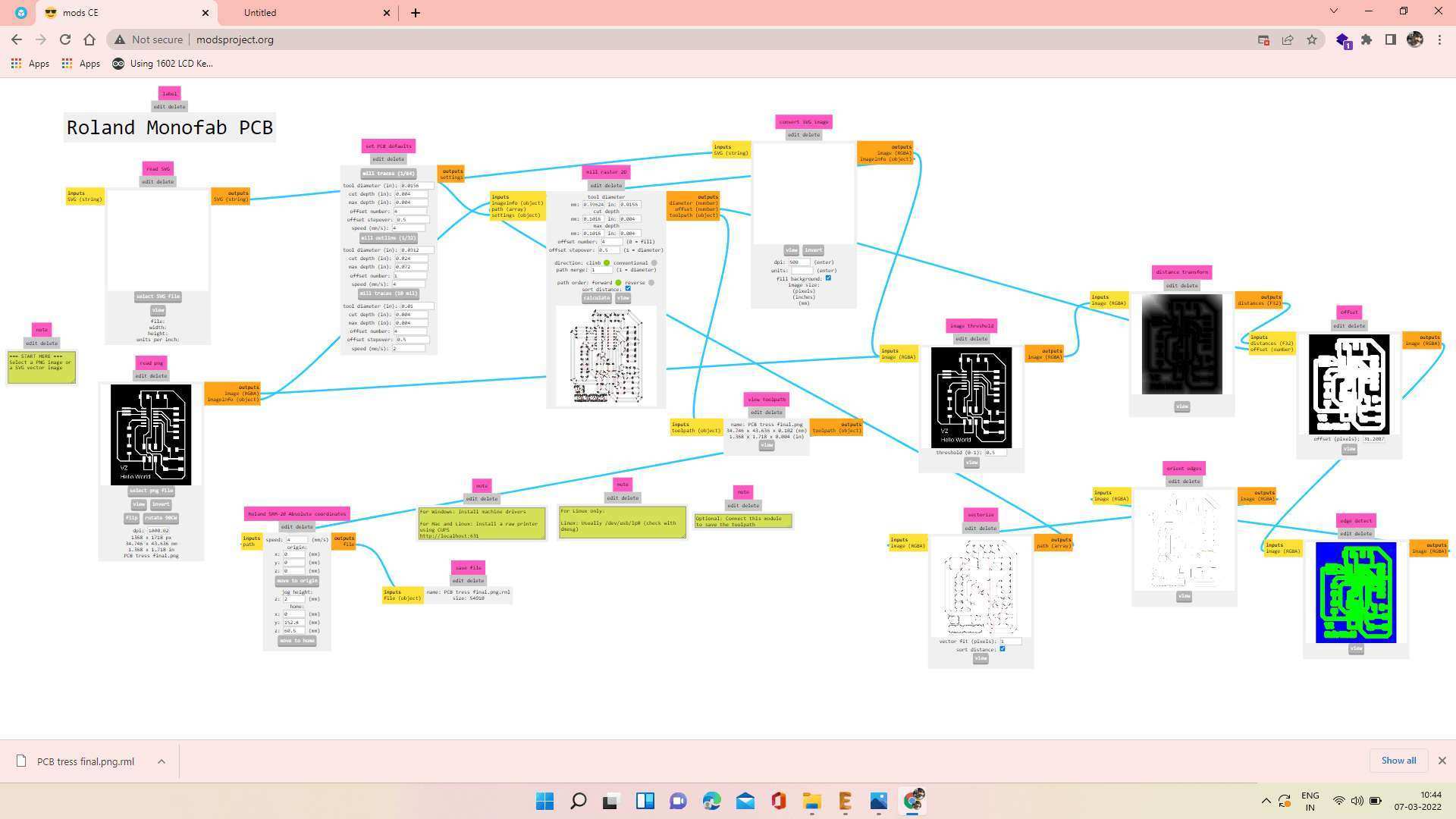
.
This is the second outer cut file I generate in mods for cutting the border of PCB.
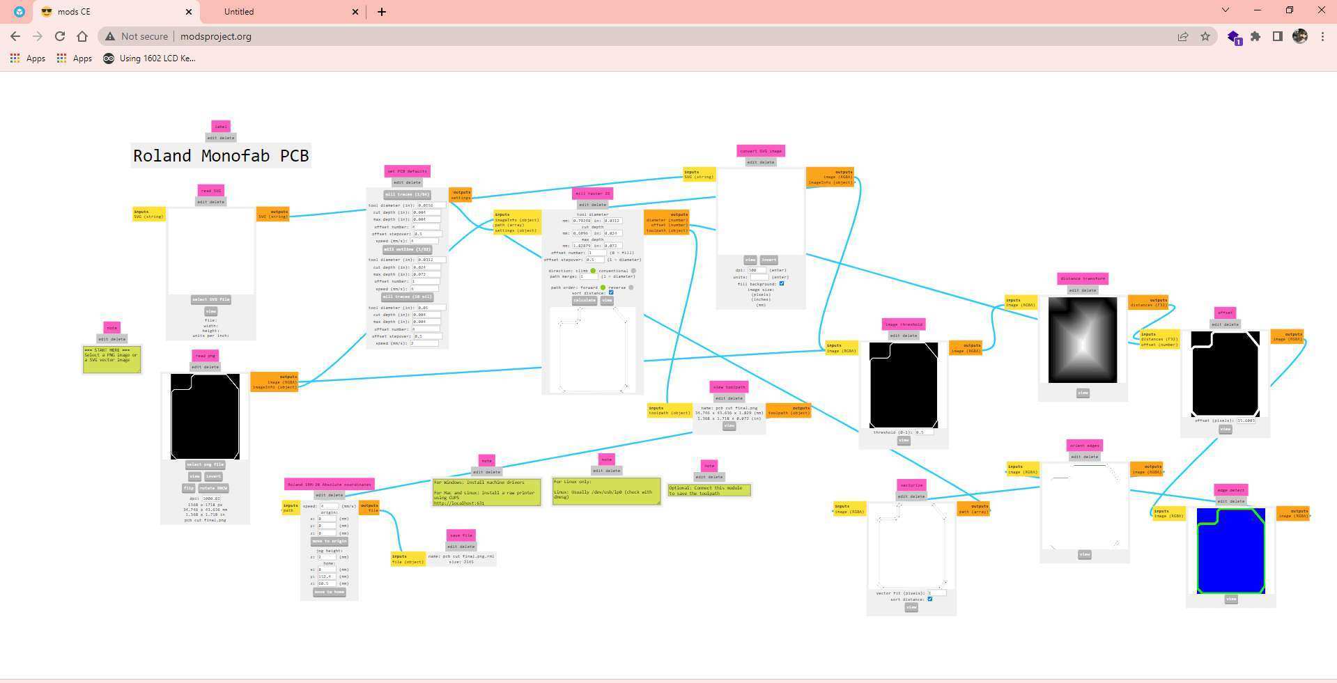
.
PCB milling .
.
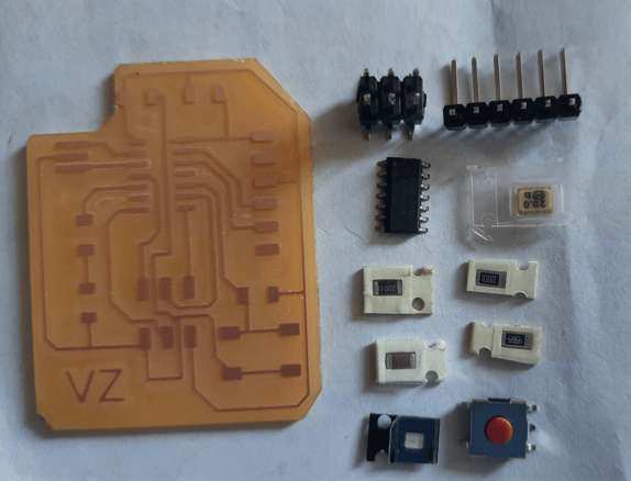
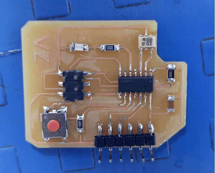
Soldering Hellow world bord
.
.
Programing the Hello world bord LED.
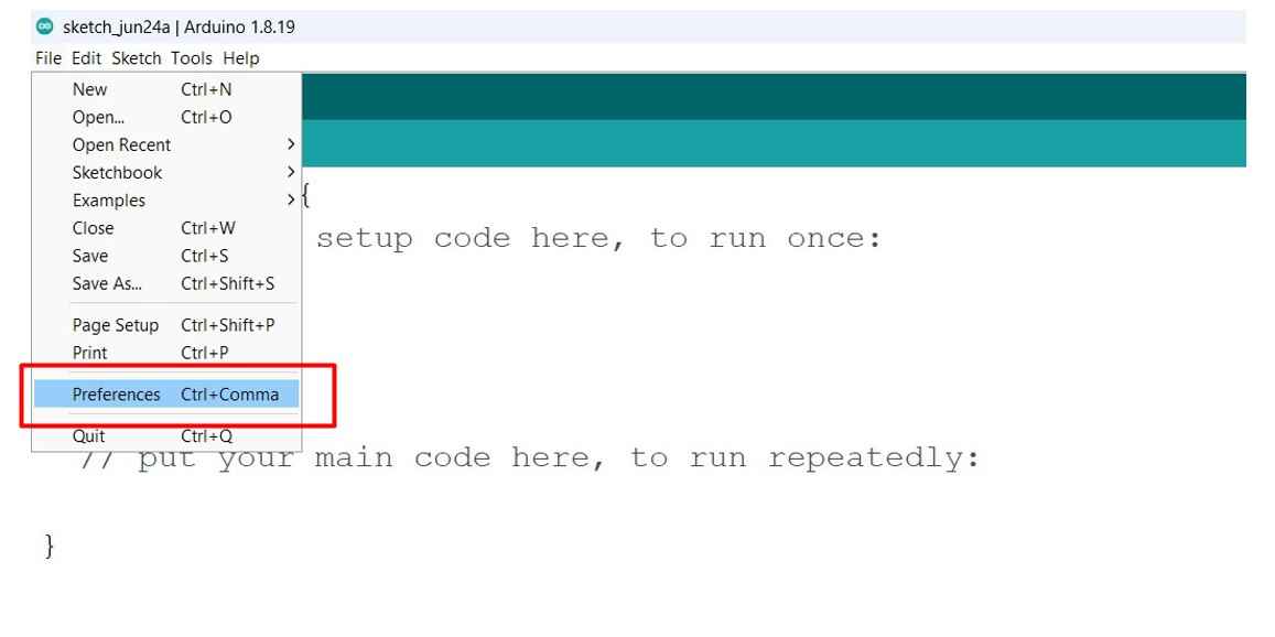
I already have an Arduino IDE installed on my system. One can download and install it here.
For programming, I have to install the ATtiny44 library In Arduino IDE. For that, I refer to This blog from MIT High Low Tech.
-
These are the steps I follow:
Step1:Go to Files >Preference
-
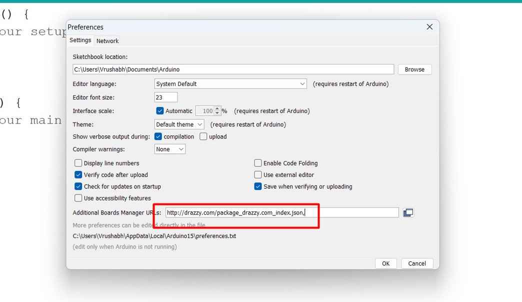
Step2: add the below link to Add Board manager URL
http://drazzy.com/package_drazzy.com_index.json
-
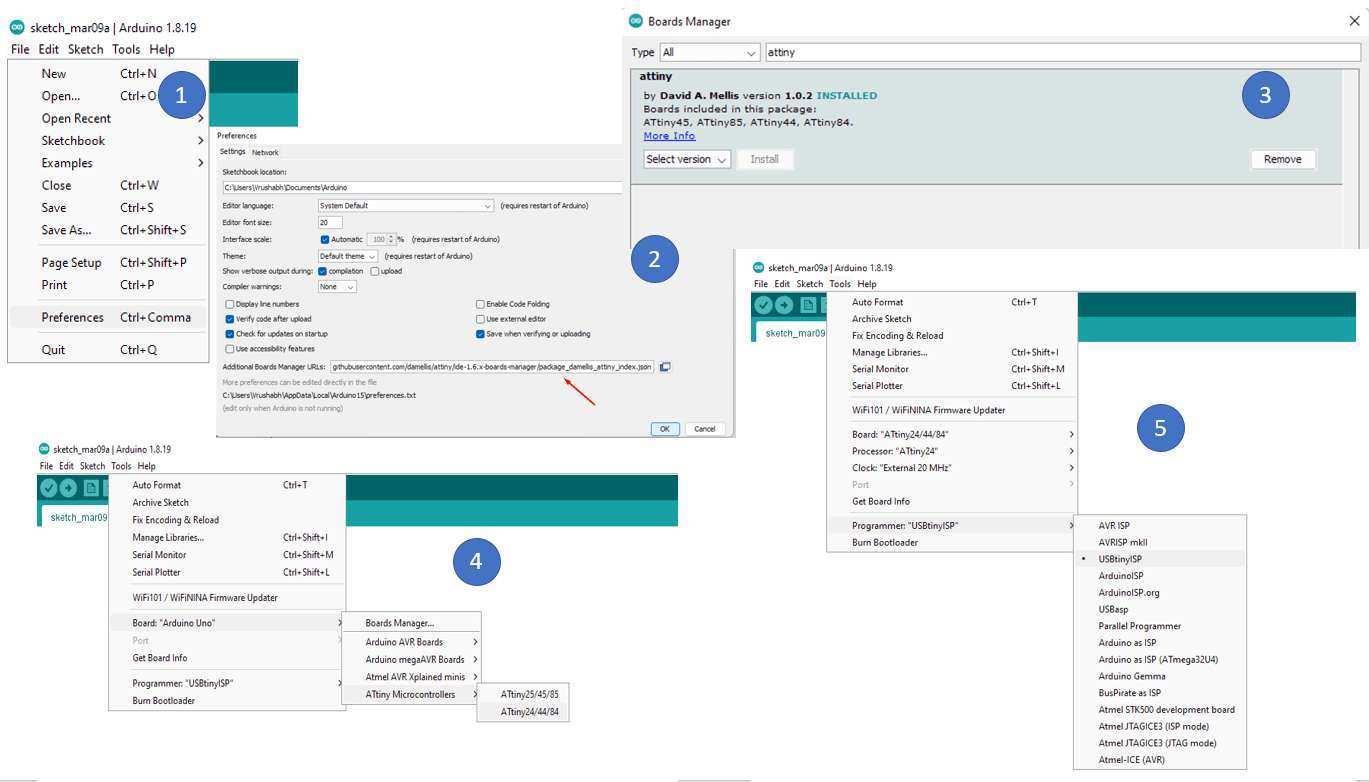
Step3:Go to Board>Boards Manager
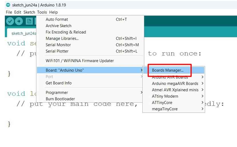
-
Step4:find ATtinyCore liberty and install it.
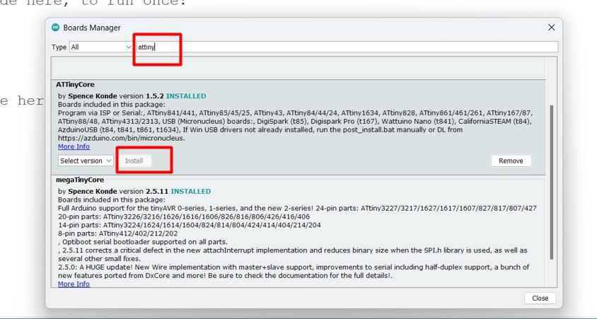
-
Step5:Go to Tool>Bords>ATtinyCore>ATtiny24/44/84.
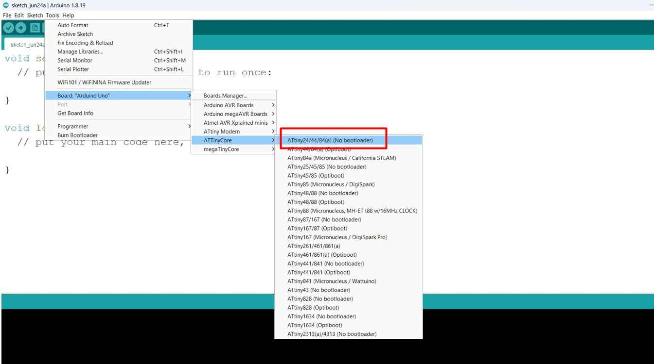
-
Submmery:
Code for LED and Butten
    /*
  Button

  This code is  Custom for Attiny 44 base hello world pcb  blink program for my fab academy assigment
*/

// constants won't change. They're used here to set pin numbers:
const int buttonPin = 3;     // the number of the pushbutton pin
const int ledPin =  8;      // the number of the LED pin

// variables will change:
int buttonState = 0;         // variable for reading the pushbutton status

void setup() {
  // initialize the LED pin as an output:
  pinMode(ledPin, OUTPUT);
  // initialize the pushbutton pin as an input:
  pinMode(buttonPin, INPUT);
}

void loop() {
  // read the state of the pushbutton value:
  buttonState = digitalRead(buttonPin);

  // check if the pushbutton is pressed. If it is, the buttonState is HIGH:
  if (buttonState == HIGH) {
    // turn LED on:
    digitalWrite(ledPin, HIGH);
  } else {
    // turn LED off:
    digitalWrite(ledPin, LOW);
  }
}