Electronics Production

Group Assignment
files to download
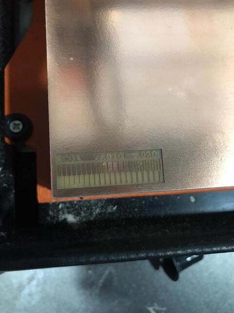
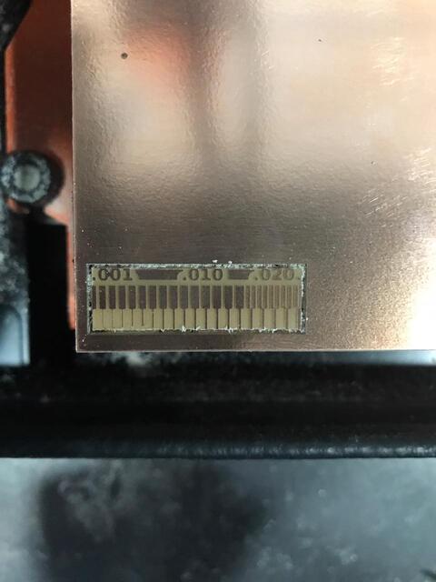
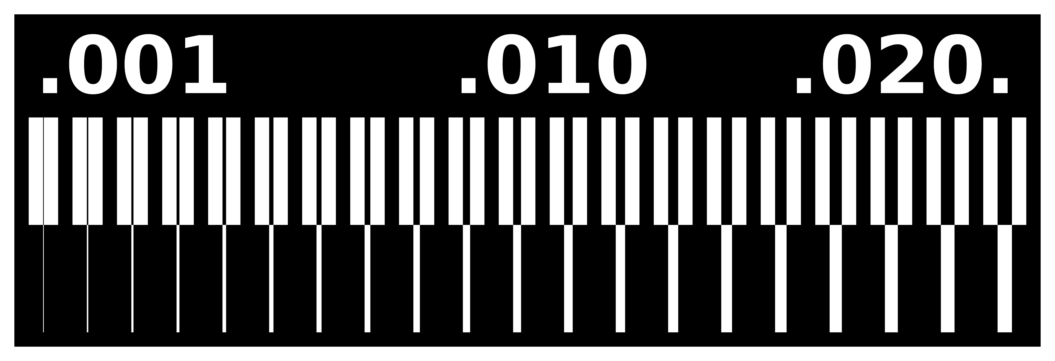
- Trace width test “traces” png file
- Trace width test “traces” rml file
- Trace width test “interiors” png file
- Trace width test “interiors” rml file
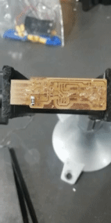
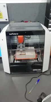
in the group assignment we learn how to use Roland monoFab SRM-20 milling machine to make PCBs In the same context we make a trace width test on a single layer PCB and I will explain it step by step below
The PCB
as a part of this assignment we use FR1 PCB material is one of the best materials to use to design and fabricate the type of single-layer printed circuit board (PCB) that you like. Despite the differences between FR1 PCB material and FR4 PCB material, PCB consumers still prefer FR1 PCB.
to fix the PCB in a proper way we unpacked the PCB bed then choose the most flat surface to fix the PCB on it
- Simplified Design for single layer PCB
- Low cost with PCB
- Excellent Mechanical and Electrical Properties
- Mechanical Drilling can do on FR1 PCB
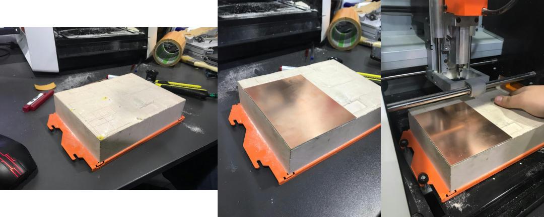
to fix the PCB board to the machine bed we use double face tape and cut around it. Remove the lower paper of the double face and fix the board on the flat surface, not above the holes or crushed surface to increase the friction as much as possible, this will make the milling process stabel and will come out a nice board
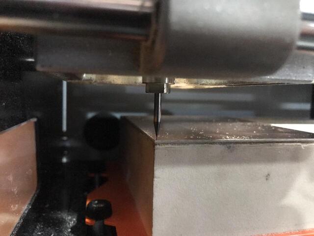
Milling Bits
We used two milling bits; for traces 1/64in (0.4 mm), and for cutting 1/32in bit (0.8 mm).
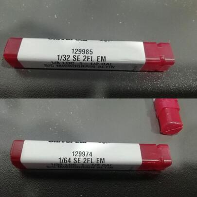
the 1/64 has a cover because it's too thin
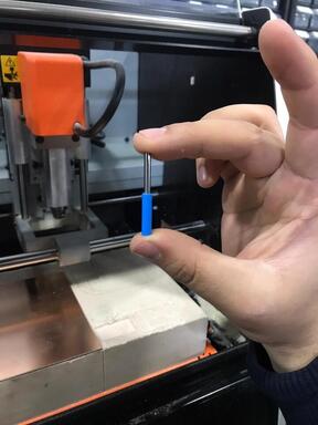
so we have to install the tool then unpack the cover
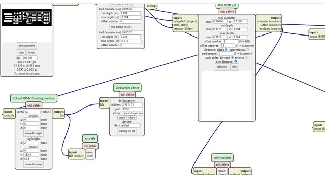
Mods
we use Modsto generate xml file which is the extension acceptable in Roland machine and to generate this file the input file could be ping, but before generating process traces and cut must be considered because we have different settings and different tools for each one so we must design the process and the frame separately
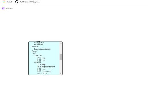
open mods and right click on the screen then choose programs > open server program > machines > Roland > mill > SRM - 20 > PCB png
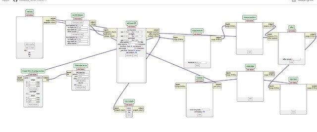
upload your circuit layout by choosing file on read png block
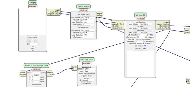
make sure that you choose the proper setting for your machine and for your material in my case (1/64 for traces and 1/32 for cutting)
then set the origin of your circuit to X 0, Y 0, Z 0
then press calculate and download your roland ready file
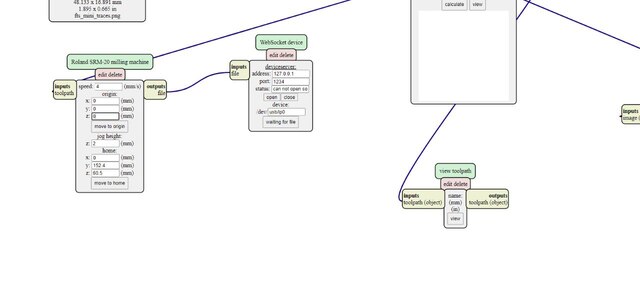
VPanel for SRM-20 software
now after preparation is done let's take a look at the software in this software you can upload the rml file and control the machine and monitor the machine behavior and it have the folwing components
- XY arrows to move and control the bed horizontally
- Z arrows to move and control the head vertically
- XYZ panel to monitor the head position according to the origin point
- speed panel to monitor the head speed in mm/min
- Spindle panel to monitor the tool speed in rpm/min
- cursor step where you can control the head move step size if its continuous the head will keep moving while you pressing the button otherwise will move steps and each of them will have a size according the number that you choose
- move panel you can move the head to the origin that you specify befor in XY or in Z
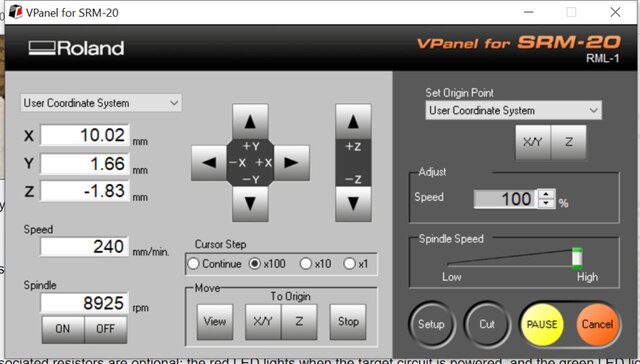
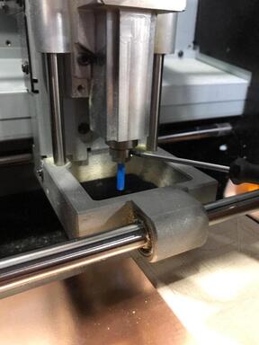
after we recognized the VPanel software lets learn how to set a new origin to use it later
in the beginning, move the bed horizontally to the point that you want using XY and press the X/Y button on right arrows after that move the bed vertically " slowly and carefully and be aware to dameg the tool, use small steps to do that " than before that the tool touches the PCB unscrew the tool screw and put it down with your hand then tighten the screw again, now set the Z origin using Z button on the right now you the machine is ready to mill
now let's upload your design into software to make the PCB traces first
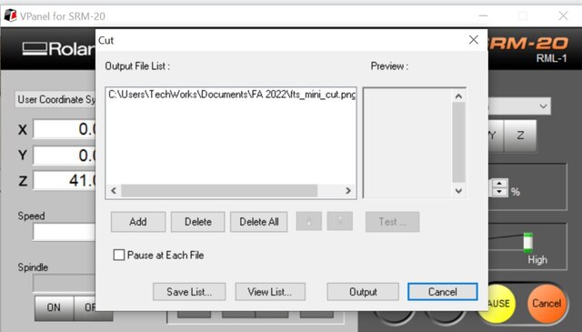
press the output button and the machine will begin in milling process
the next step is to cut the PCB but before we have to change the tool as we describe before
individual assignment
files to download
Google Drive
- FabTiny ISP “traces” png file
- FabTiny ISP “traces” rml file
- FabTiny ISP “interiors” png file
- FabTiny ISP “interiors” rml file
direct link
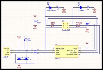
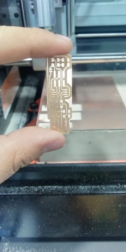
Below is the schematic and layout of the ISP PCB programer and I will list the needed component for this circuit note that all components are SMDs.
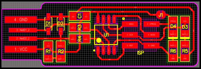
I followed the same steps described in the group assignment and made my ISP programmer PCB. For “offset number” I put 5 to make traces without a long time in milling.
before soldering let's recognize the components that we need for this circuit
list of component
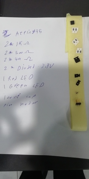
- ATtiny45 x1
- 1kΩ resistors x2
- 499Ω resistors x2
- 49Ω resistors x2
- 3.3v zener diodes x2
- red LED x1
- green LED x1
- 100nF capacitor x1
- 2x3 pin header x1
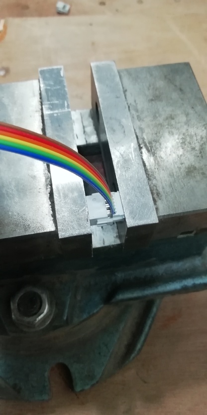
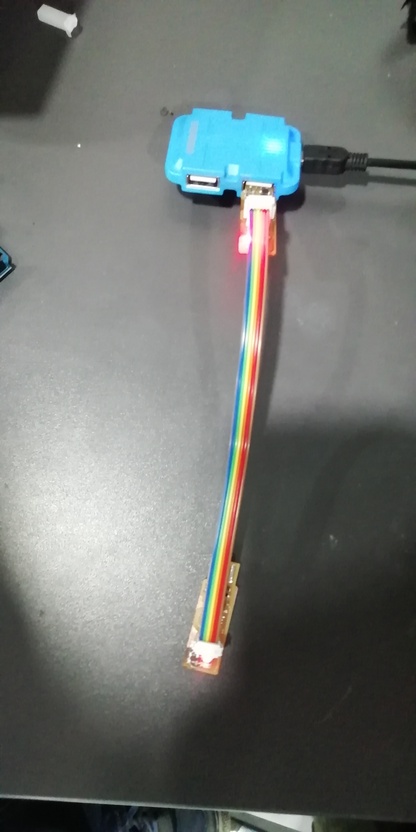
before programing process i made the ISP cable which will require 2x3 female pin header x2 and cable
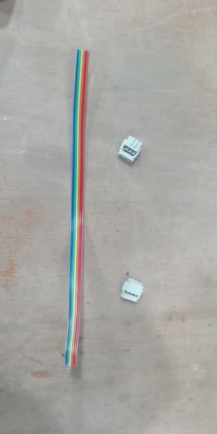
butt the connecters opposite to each other to make sure that you have the right connection
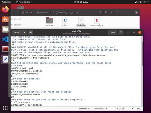
Development Environment (ubuntu 20.04)
to program, the ISP programmer follow the steps below
Step 1: Download “Atmel AVR Toolchain for Windows” ZIP file. Extract it in certain place that you specify
Step 2: then edit the "make" file and butt your programmer name in my case is "usbtiny"
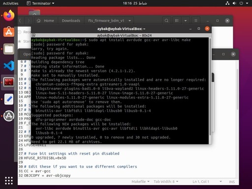
Step 3: now close the make file and install the "avrdude" enter the following command, followed by your password when prompted: sudo apt install avrdude gcc-avr avr-libc make
Step 4: now connect the programmer to your board and make sure that you are in the correct orientation
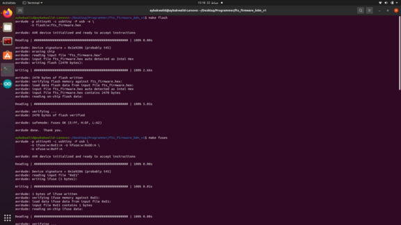
Step 5: make This will build the hex file that will get programmed onto the ATtiny45. When the command completes, you should now have a file called fts_firmware.hex.butt before exute this command go to the fts_firmware_bdm_v1 file using cd command v
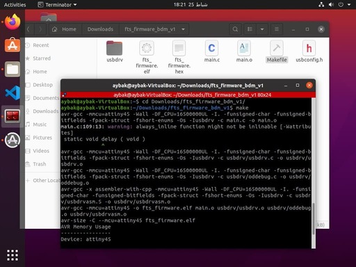
Step 6: make flash This will erase the target chip, and program its flash memory with the contents of the .hex file you built before
Step 7: make fuses This will set up all of the fuses except the one that disables the reset pin
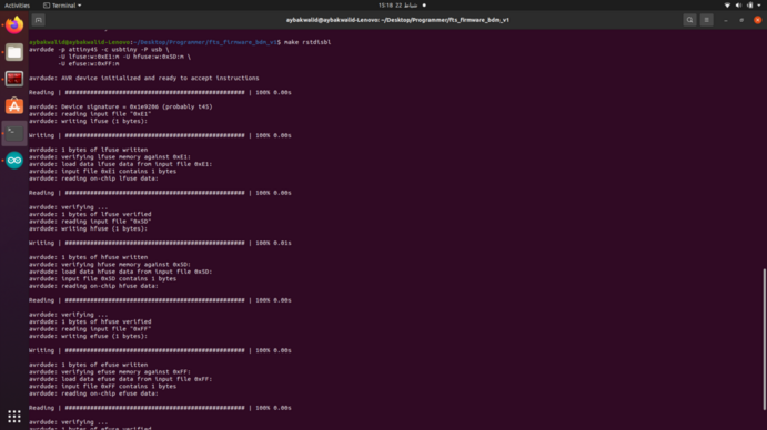
Step 8: make rstdisbl his does the same thing as the make fuses command, but this time it's going to include that reset disable bit as well.
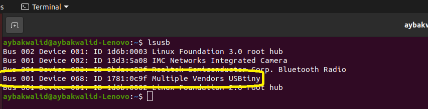
Step 9: lsusbthe last step is to check if the programmer is identified as an external device.
to do so go to the terminal and type lsusb
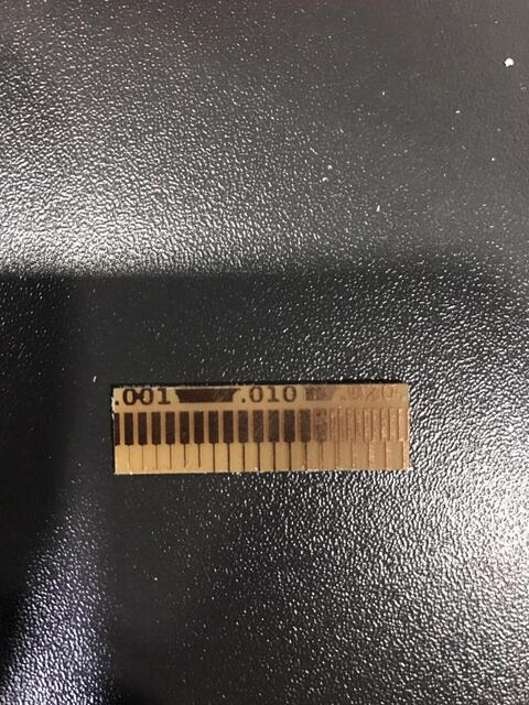
Hero Shot