5. Electronics production
Assignment
group assignment
-
characterize the design rules for your in-house PCB production process
-
extra credit: send a PCB out to a board house
individual assignment - make an in-circuit programmer that includes a microcontroller:
-
extra credit: customize the design
-
mill and stuff the PCB
-
test it to verify that it works
-
extra credit: try other PCB processes
Tools Used at 3DEXPERIENCE Lab at Dassault Systèmes
Machines
Software
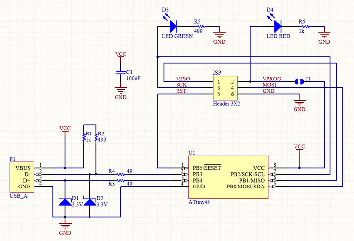
Components
-
PCB
-
1x ATtiny45 or ATtiny85
-
2x 1kΩ resistors
-
2x 499Ω resistors
-
2x 49Ω resistors
-
2x 3.3v zener diodes
-
1x red LED
-
1x green LED
-
1x 100nF capacitor
-
1x 2x3 pin header
Tools
-
Weller WES51 Soldering Iron
-
Curved Tweezers
-
Soldering Tip Cleaner
-
Carpenter’s Tape
Group Assignment
Characterize the design rules for your in-house PCB production process
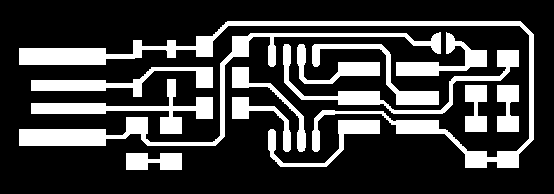
Resources we used to create the Trace and cut of the Board
Together we chose to make a FabTinyISP, and we used Brian’s page as a guide.
How to create the the board files:
-
Go to Building the FabTinyISP
-
Download the PNG files for the traces and the board outline:
-
Go to mods.
-
Click > Programs > Open Server Program
-
Roland > Mill > SRM-20 > PCB .png
-
Select WebSocket Device, and delete by clicking on inputs and outputs until red line disappears. Choose delete.
-
Connect to be able to save.
-
We determined the Roland Device needed to have the following settings to allow for the board to be cut correctly.
Here is the process we went through to cut and mill the board:

Individual Assignment
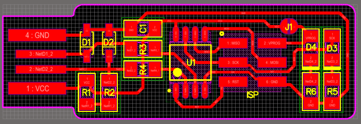
Make an in-circuit programmer that includes a microcontroller: mill and stuff the PCB and test it to verify that it works
In 2017, before I started Graduate School I worked with Circuit-Lab for the summer. It was a wonderful, and my first deep dive into electronics. Fortunately, I had experience/familarity in understanding the board image, and the schematic. With my limited soldering experience in the past I was thrilled to jump in and get going.
As I did not have enough time to complete soldering the board in the lab and I took it home with me, as I had a soldering iron.
After two days, I completed the board, as I made mistakes that I will share below.

I plugged the board into my computer to run a smoke test and it passed, success!
Mistakes I made, and how I resolved them
Mistake 1
I added too much lead to the legs of various components, and it leads…no pun intended…to connecting unwated paths. As seen in this image.

Fix
Soldering braid for desoldering. Soldering braid when heated can help lift solder. Since it was President’s Day Weekend and the lab was closed, I headed to Microcenter and purchased Super Wick, and any soldering braid should work.
Mistake 2
You have too much lead on your soldering tip.
Fix
Clean it off using a Tip Cleaner.
Mistake 3
Don’t forget…there is extra copper on the edge of your board where you connect the board into the USB port.
Fix
- Use a razor and tweezers to peel the copper away.
Process Hack
- Add double-sided tape to Post-It with list to attach components to it to stay organized.