Task to be carried out this week
Action Plan
| Date | Work Allocation |
| 2nd March | Prof. Neil's Lecture |
| 3rd March | Learning about the basic electronic components and electronic design |
| 4th March | Learning to use the eagle software |
| 5th March | PCB design using autodesk eagle software |
| 6th March | Milling my PCB |
| 7th March | Soldering the components on my PCB |
| 8th March | Documentation |
Introduction to Electronic Components and Electronic Design
1. Ribbon Cable:A cable for transmitting electronic signals consisting of several insulated wires connected together to form a flat ribbon.
2. IDC connectors: Insulation-Displacement Connector(IDC) are electrical connectors designed for ribbon cables and telecommunications applications. They are also referred to as insulation-piercing contacts (IPCs).
3. Buttons:Buttons and switches are among the most basic but necessary components in an electronic project. They can be of many types such as slide switches, push button, toggle button, rotary switches, etc.,.
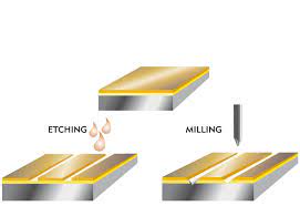
4. Printed Circuit Boards(PCB):A printed circuit boards (PCB) are foundational building block of most modern electronic devices. It is used to mechanically support and electrically connect electronic components using conductive pathways, tracks or signal traces etched from copper sheets laminated onto a non-conductive substrate.
There are two ways to add components on PCB:
PCB circuit design using Autodesk Eagle Software
Autodesk EAGLE is a scriptable electronic design automation (EDA) application provided by autodesk company. EAGLE stands for Easily Applicable Graphical Layout Editor. It provides options to create schematic as well as board circuit design. The schematic files are saved with .sch extension and board files as .brd files. We can also export the board files as .png image files. I had learned basic electronics in my college days, but I had forgotton most of it. I had to re-learn most of the things but I was able to grasp easily. This was the first time I used the eagle software and I found the process to be quite interesting. However, I faced trouble when trying to arrange the components in my board design. I found this part to be quite difficult and confusing
To begin, I forst installed the eagle software. Once I was done with the installation, I downloaded the fablibrary from the GIT account. Fab library contained most of the electronic components that we were to use in fab academy and for the week's assignment.
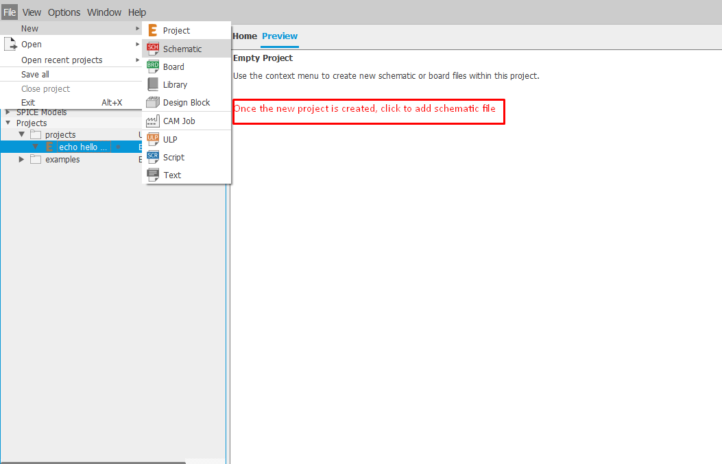
I extracted the libraries from the downloaded zip folder. Next,I opened the eagle software and created a new file.
To do that open eagle software → Click on files → new → Project and name your project.
Now once the project is created, go to files → new → schematics to create the schematic diagram of the circuit.
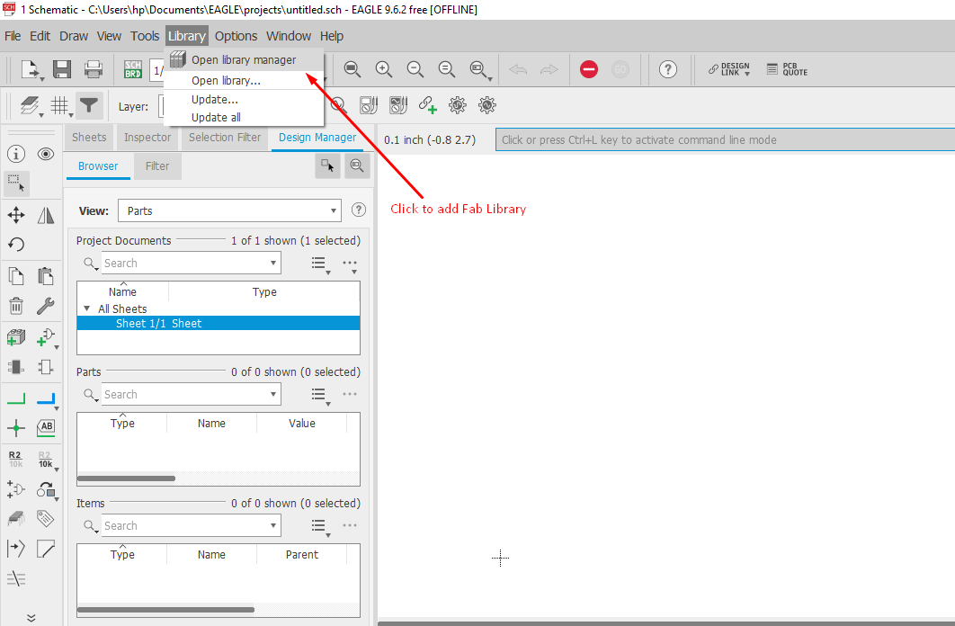
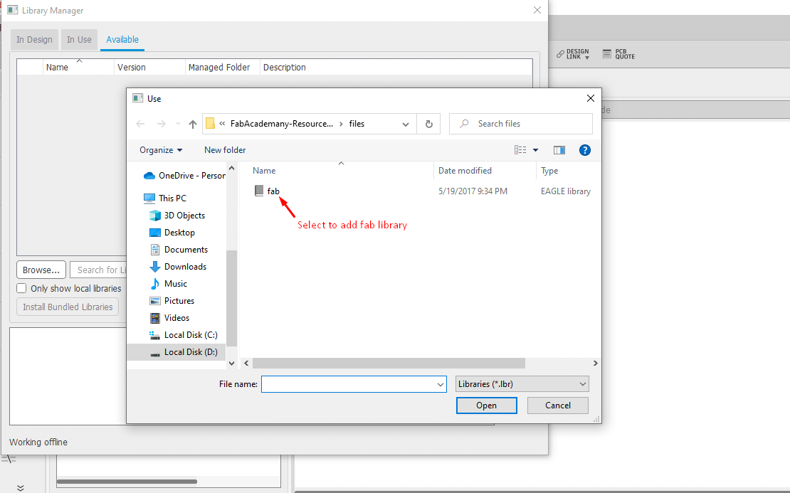
Next, I had to add the fab library to the project I created. To do that
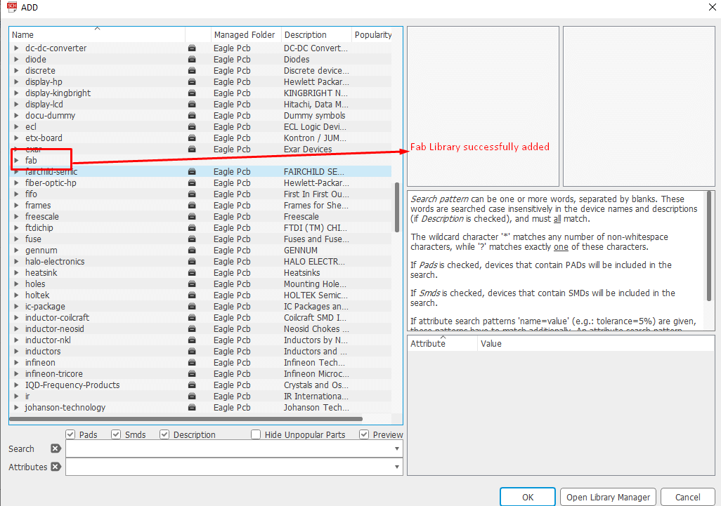
Go to Library → Open Library Manager → click on browse → select the fab library → click use.
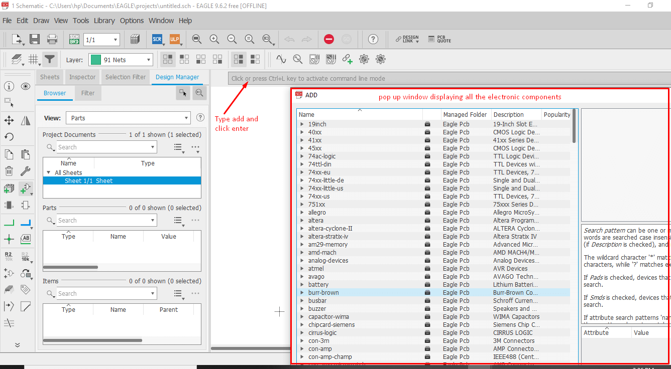
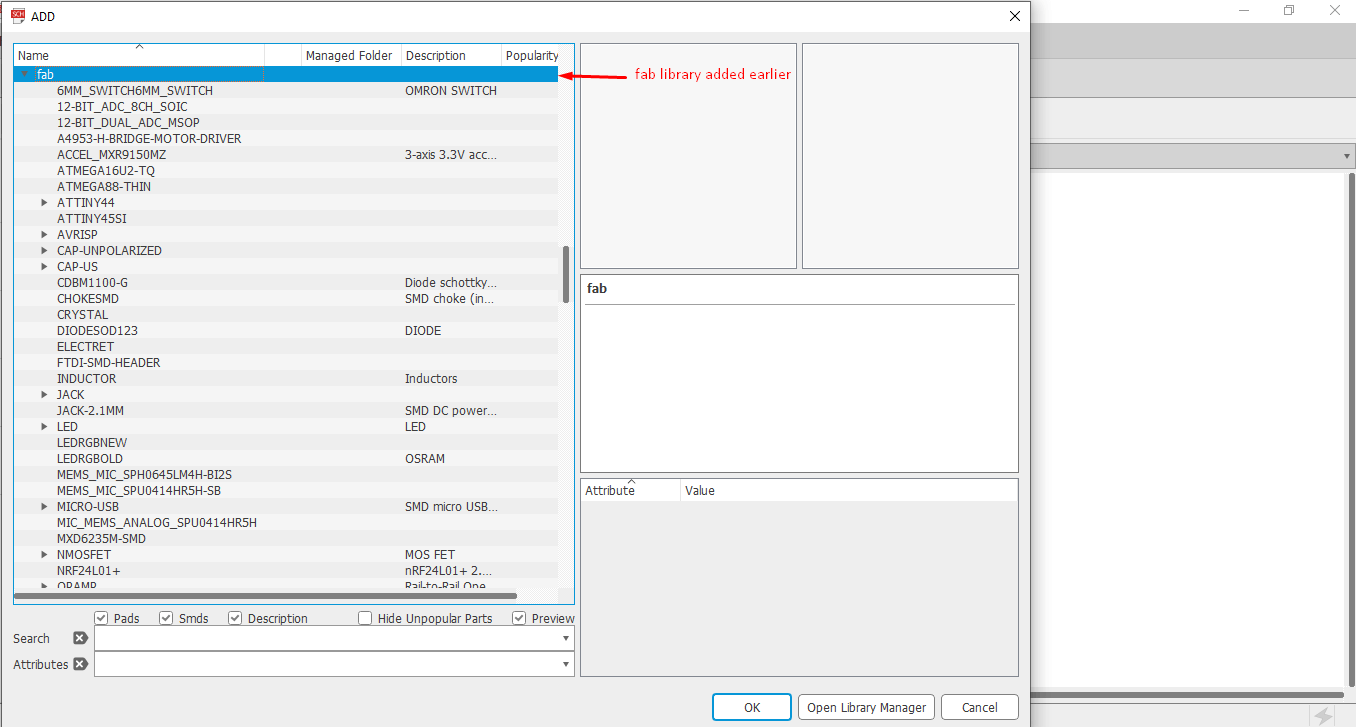
Once I was done with setting up the library, I started to draw the schematic diagram for eco-hello board. To add the components, type 'add' on the text bar as shown in image below. On entering, we get a pop-up box displaying all the components. Since we have already added the fab library, we can now use the components available under fab library to draw our schematic diagram of the echo hello board.
For making my echo hello board, I used the following components;
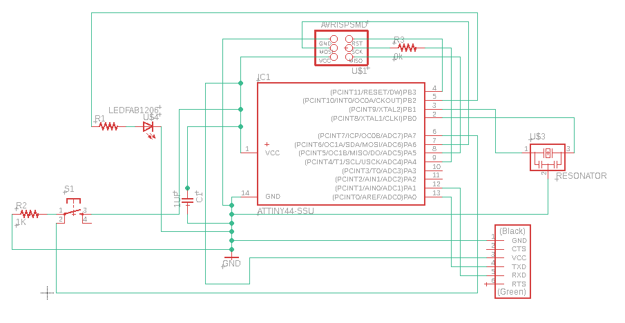
This was the final schematic design I made.
Next I generated the board design from the schematic design. To do that click on the icon as shown below. Once I generated the board design, I moved all the components to the design window of the board design. I stared arranging the components based on the best possible fit. Then I manually routed the connections. There were a couple of design rules I had to keep in mind when routing. First, I had to change the trace width to 16. I could do that by clicking the width option in the task bar above the design window. Our lab instructor informed us to ensure that no traces/routes run in between the controller pins and no more than 2 routes should run under any components. I started routing and it took me an entire day and a half to optimize my board design to 100%. I had to add a zero ohm resistor to optimize my routinng. In the week's assignment, I found this task to be the most difficult and it required a lot of patience which I lacked. However after trying for a 100th time I was finally able to design my board diagram. Following is the final board design I made;
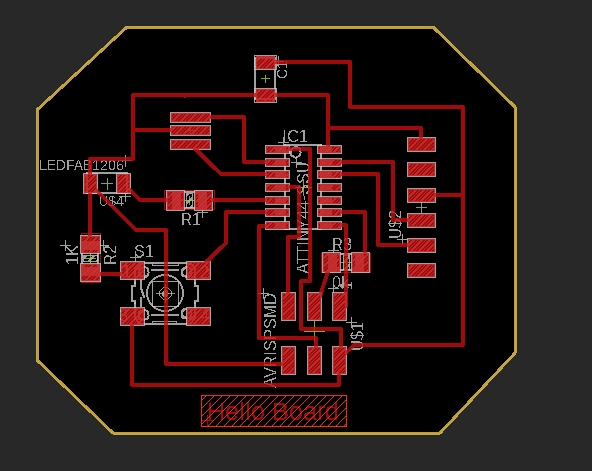
I believe the the design is still lacking and need better routing but I am happy that I was able to atleast fulfill the basic design rules and create the a functional board diagram. I hope to improve my skill as I keep using the software
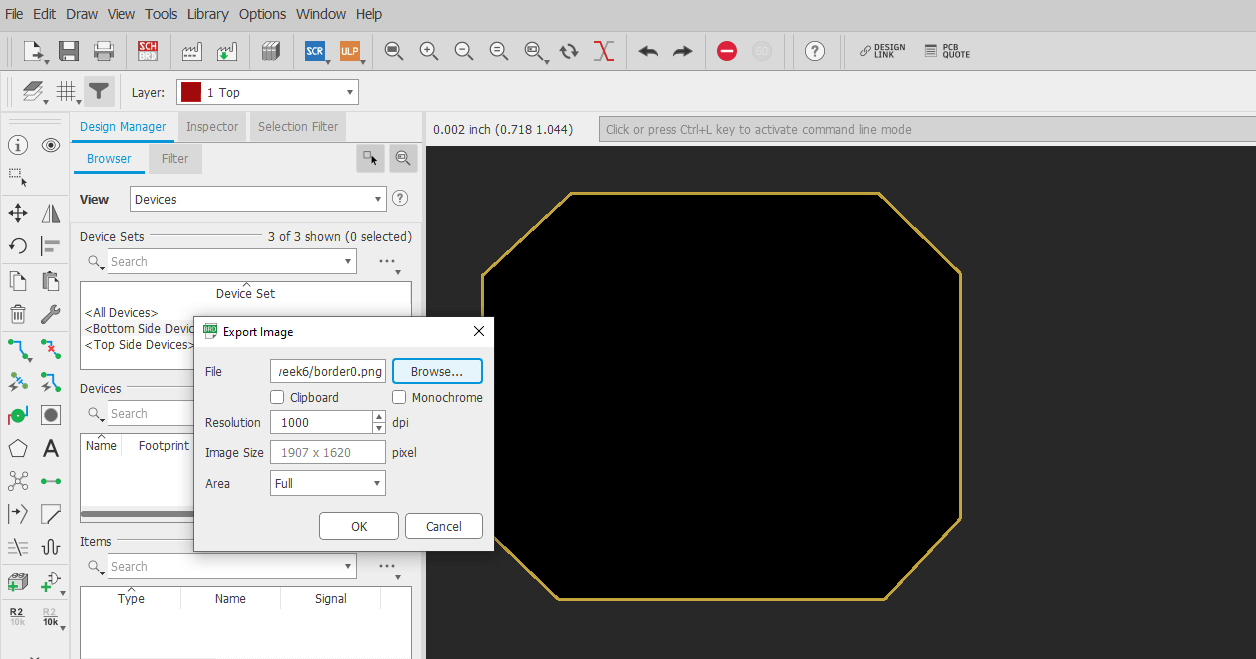
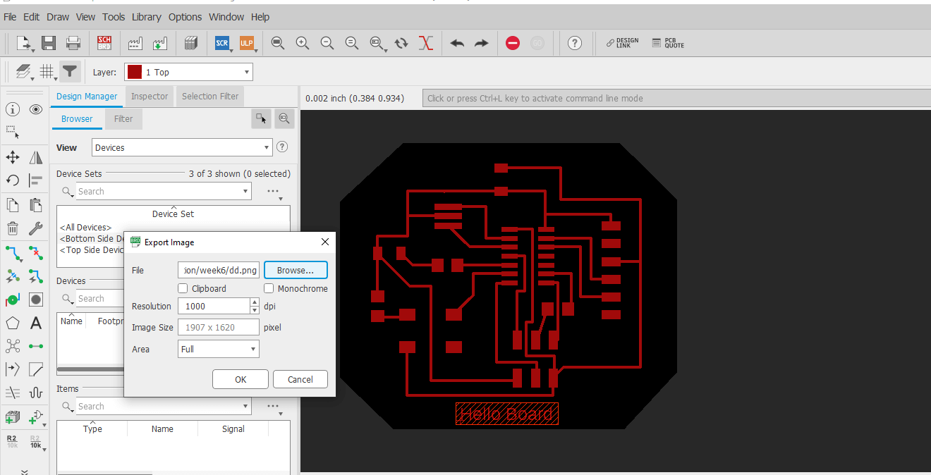
Next I exported the board design as .png file. Before exporting, I removed the labelings on the components. This needs to be done to avoid issues when milling the pcb. To do that;
Go to view option → Select layer setting → hide all the layer except for dimensions layer for border traces and top layer for design traces.
To export the design go to Files → export → select image → name the image the save. We need to save the border file and traces file seperately. Please ensure to save the image file with a minimum resolution of 1000. I didn't change my resolution in the begining and it gave problems when milling.
Printing the Echo Hello board
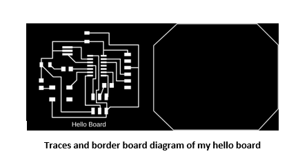
For printing my echo hello board, I followed the steps used during the Electrinic production week. I printed my board using the Roland SRM20 machine and used MIT Mods to create the machine readible .rml file. I tried printing my board but it didn't get printed well. The milling was not done properly.
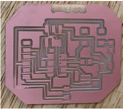
This happened because I have saved my image file with very less resolution. Thus, I created a new .png image file with highter resolution and printed the board again. This time the board was printed cleanly. Once I was done printing my board, I started with the soldering process. I soldered the components on the board following the steps and process learned during week 4. This was the final board after soldering.
Programming my echo hello board\
The second part of the assignment for the week was to program the echo hello board. We used audrino as programmer to program the echo hello board.
To do that, I had to first undertand the pin layout of the arduino and ATTiny 45. I found the pin layout online and I followed the layout to make connection between the arduino and ATTiny 45 microcontroller.
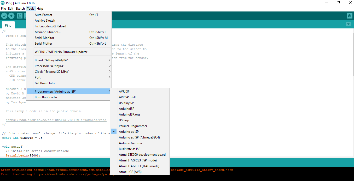
We used the Arduino IDE software to program the board. Before programming, we had to first select arduino as the programmer in the Arduino IDE. To do that;
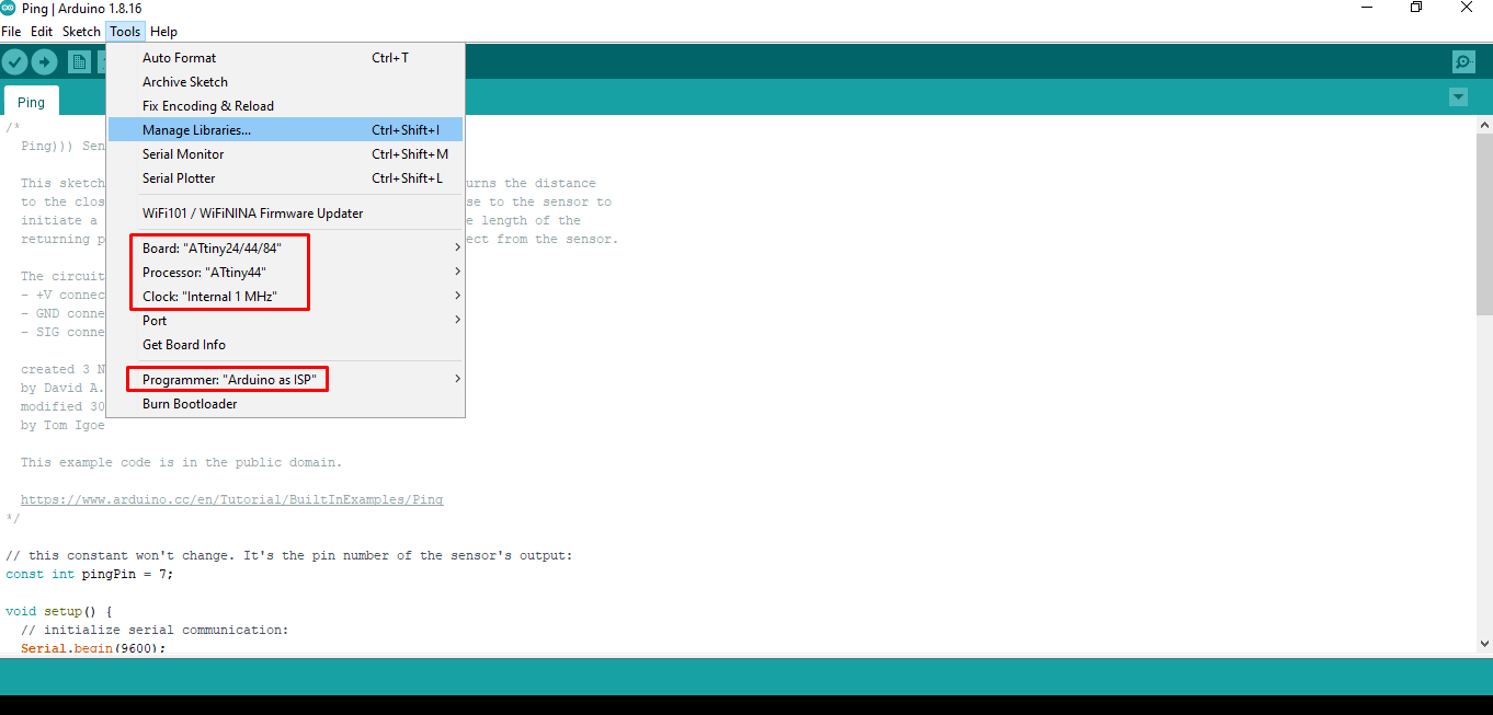
Go to Tools → Programmer → select Arduino as ISP.
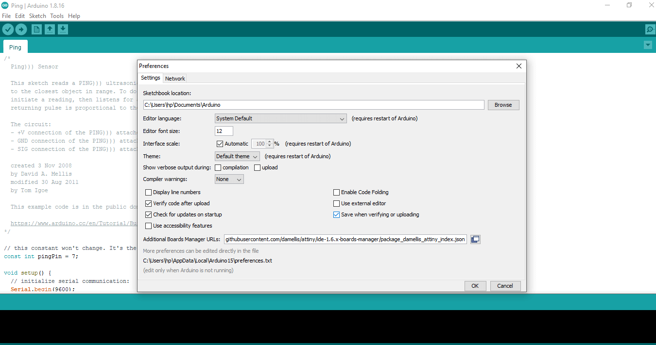
Next we have to choose the board to be programmed. Since our board option is not available on Arduino IDE, we need to download and add the board to the Arduino IDE library. To do that Go to Files → Preferences → paste the ULR for additional board manager. The file for the additional board manager can be found on Github
Now that the board is available on the Arduino IDE, we select the board to be programmed, th Arduino ISP as the programmer, ATTiny 44 as the processor and set the clock to 1MHz on Arduino IDE.
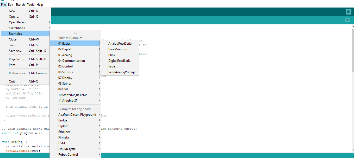
Next we use the following program to check if the board is programable or not. We use a simple LED blinking program which is already available under examples on the Arduino IDE. I just had to change the output pin number.
This was the video of the working programmed echo hello board.