Electronic Production
PCB Milling
Printed Circuit Board, or PCB milling is the practice of using a computer controlled mill to engrave and cut out circuit boards. Simmilar to other forms of digital fabrication, CNC milling follows a simmilar workflow. Step one is to use a CAD software to design the circuit board, step 2 is to use a CAM software to covert the design into a form of G code understandable by the mill, and step 3 is to set up the mill and cut the board. This is the practice of designing a board no matter the context, however often times the CAM and milling step is outsourced to a company such as OSHPark who will receive the CAD design and send you back your milled board.
Printed Circuit Board, or PCB milling is the practice of using a computer controlled mill to engrave and cut out circuit boards. Simmilar to other forms of digital fabrication, CNC milling follows a simmilar workflow. Step one is to use a CAD software to design the circuit board, step 2 is to use a CAM software to covert the design into a form of G code understandable by the mill, and step 3 is to set up the mill and cut the board. This is the practice of designing a board no matter the context, however often times the CAM and milling step is outsourced to a company such as OSHPark who will receive the CAD design and send you back your milled board.
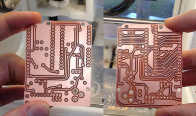 Non Commercial One Sided PCB
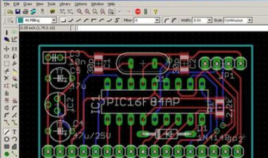
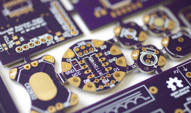 OSH Park PCB
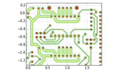
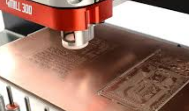 Consumer PCB Mill
Designing a PCB
In order to design a PCB we need to use some sort of CAD software. For this week the boards being milled were already designed for us, however it is still important to know how they were made. There are various softwares available for design PCB boards, including Fusion, Eagle, Altium Designer, and more. However one of the most popular hobbyiest PCB CAD softwares is KiCAD, due to it being Free and Open source, and recently publicly supported by CERN who have made large donations to improve it's effeciency, tools, and UI.
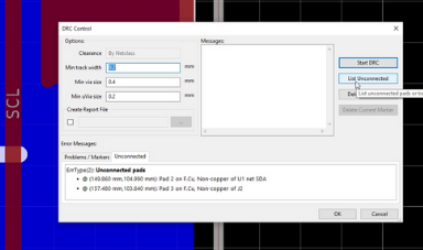
These PCB CAD Softwares have two main modes schematic mode and board mode. In schematic mode one can make a standard electornic circuit as seen in any circuits class. Everything will be drawn with standard notation, labeled with the appropriate labeles and all connected together with potentially crossing wires in however the designer designs to layout their schematic. This is the first step, and lays out the components and connections for you board, however is not enough. Following that step comes board mode where either manually or using an autorouter proper non intersectring traces get routed and layed out on the board. Each component will have now have their respective footprints instead of their standard notation, and the traces will effeciently and properly connect everything as needed in sometimes non-intuitive layouts. In this step however it is important to know the max size of your traces, and how far away they have to be from one another. There are various factors in detemrining this, but the main one and the only one of interest for most beginner projects are the limitiations of the mill itself. It's not possible to design a board with traces .5 mm apart when the smallest bit available is 2mm. This information is inputted into whats called a DRC (design rules check ). This will check your board before finsihing to make sure its possible to mill, and can be inputted into the autorouter software to rout the traces according to the DRC. Later on in this project we will be detemrining some information that will help us make a proper DRC for our machine.
In order to design a PCB we need to use some sort of CAD software. For this week the boards being milled were already designed for us, however it is still important to know how they were made. There are various softwares available for design PCB boards, including Fusion, Eagle, Altium Designer, and more. However one of the most popular hobbyiest PCB CAD softwares is KiCAD, due to it being Free and Open source, and recently publicly supported by CERN who have made large donations to improve it's effeciency, tools, and UI.
These PCB CAD Softwares have two main modes schematic mode and board mode. In schematic mode one can make a standard electornic circuit as seen in any circuits class. Everything will be drawn with standard notation, labeled with the appropriate labeles and all connected together with potentially crossing wires in however the designer designs to layout their schematic. This is the first step, and lays out the components and connections for you board, however is not enough. Following that step comes board mode where either manually or using an autorouter proper non intersectring traces get routed and layed out on the board. Each component will have now have their respective footprints instead of their standard notation, and the traces will effeciently and properly connect everything as needed in sometimes non-intuitive layouts. In this step however it is important to know the max size of your traces, and how far away they have to be from one another. There are various factors in detemrining this, but the main one and the only one of interest for most beginner projects are the limitiations of the mill itself. It's not possible to design a board with traces .5 mm apart when the smallest bit available is 2mm. This information is inputted into whats called a DRC (design rules check ). This will check your board before finsihing to make sure its possible to mill, and can be inputted into the autorouter software to rout the traces according to the DRC. Later on in this project we will be detemrining some information that will help us make a proper DRC for our machine.
 Altium Designer
 Eagle
Eagle
 Viewing PCB in Design Mode in Fusion
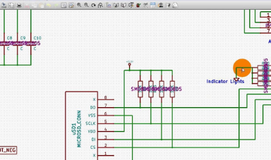 KiCAD Schematic
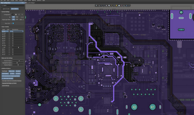
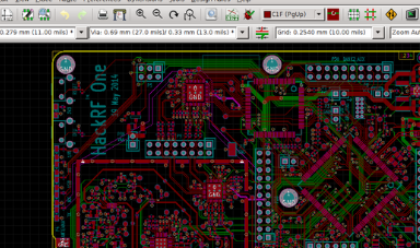 KiCAD Board View
 Design Rules Check
Layers of a PCB
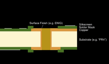
Before going on it's important to understand the different layers of a PCB board, to know what is an what is not being milled and how it works.PCB boards are made up at a minimum 2 layers, a substrate and a copper layer. The substrate is a non conductive layer typically made of fiberglass, and epoxy. It is usually flame retardent as well which is why people call it FR4, or flame retarded grade 4. The top layer, the copper will be the part milled where the mill will engrave around the traces down to the substrate layer forming traces surrounded by non-conductive material. These are the standard PCB boards most consumers will produce with their own mill. However far more layers can be added to boards when produced in proper facilities. First off it is possible to have multiple stacked layers of copper and subrate to make a multilayer board. In addition to that the exposed layers of the board, top and bottom (if there is copper there) often also get a solder mask added which covers up most of the traces else then small parts needed to solder components on to which protect the traces and makes it easier to solder. In addition on those exposed surfaces a surface finish is added which will protect the copper underneat from oxidizing. Typically then a silkscreen layer which is a type of ink to add drawings or component information on the board. Unfortunately these additional layers are a luxury of having proper companies producing boards for you, and instead we just get the two: substate and a single layer of top copper.
Before going on it's important to understand the different layers of a PCB board, to know what is an what is not being milled and how it works.PCB boards are made up at a minimum 2 layers, a substrate and a copper layer. The substrate is a non conductive layer typically made of fiberglass, and epoxy. It is usually flame retardent as well which is why people call it FR4, or flame retarded grade 4. The top layer, the copper will be the part milled where the mill will engrave around the traces down to the substrate layer forming traces surrounded by non-conductive material. These are the standard PCB boards most consumers will produce with their own mill. However far more layers can be added to boards when produced in proper facilities. First off it is possible to have multiple stacked layers of copper and subrate to make a multilayer board. In addition to that the exposed layers of the board, top and bottom (if there is copper there) often also get a solder mask added which covers up most of the traces else then small parts needed to solder components on to which protect the traces and makes it easier to solder. In addition on those exposed surfaces a surface finish is added which will protect the copper underneat from oxidizing. Typically then a silkscreen layer which is a type of ink to add drawings or component information on the board. Unfortunately these additional layers are a luxury of having proper companies producing boards for you, and instead we just get the two: substate and a single layer of top copper.
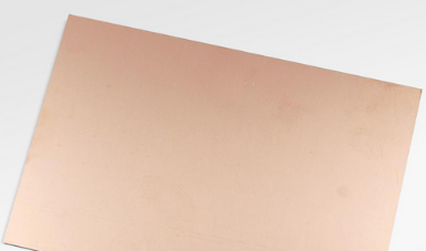 Copper Sheet to be Milled into a PCB
 Layers of a PCB
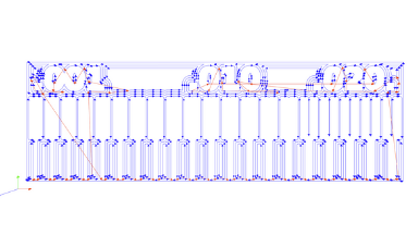
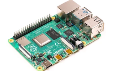 Rasberry Pi which has 6 layers of copper
CAM
With a design now made, it is time to export it to a CAM software. The CAM software will take the design of all the traces and detemrine how the mill itself will move creating a form of G-Code that the mill will understand. The first choice is to export your file as a Gerber file, a Gerber file is a file contaiing vector information relating to each layer and and location of each trace on each layer. It is the universal industry standard, and highly reliable. When sending ones design to a company to mill they expect that you send them a Gerber file. We can use a software called Flat Cam, a free open source CAM software which will read the Gerber file, and allow the user to set the appropriate milling parameters to then generate nc code, a standardized variant of g-code. Another alternative is to use the MIT software, which was then adapted by the community CAM software mods which will instead accept as an input a png black and white image of the traces. It will then run the png image through an image analaysis algorithm which will find vector information relating to the distance between the black parts of the PNG. This vector information will then be used to generate paths, and then create a form of g-code. Mods can be used witha variety of mills, in our case we select the Roland SRM-20. If the machine with Mods was connected directly to the mill it is possible to control the mill using just mods instead of the mills own control panel, however in our set up instead we still use the control panel of our mill, and instead export from mods the file by removing the last module and replacing it with a save file module. This will generate a RML file whcih stands for "Roland Media Library", a proprietery unstandard g-code variant only compatible on Roland products. In MODS all the apprpriate information can be inputted to design the proper g-code including endmill diameter, feed rate, and cut depth.
With a design now made, it is time to export it to a CAM software. The CAM software will take the design of all the traces and detemrine how the mill itself will move creating a form of G-Code that the mill will understand. The first choice is to export your file as a Gerber file, a Gerber file is a file contaiing vector information relating to each layer and and location of each trace on each layer. It is the universal industry standard, and highly reliable. When sending ones design to a company to mill they expect that you send them a Gerber file. We can use a software called Flat Cam, a free open source CAM software which will read the Gerber file, and allow the user to set the appropriate milling parameters to then generate nc code, a standardized variant of g-code. Another alternative is to use the MIT software, which was then adapted by the community CAM software mods which will instead accept as an input a png black and white image of the traces. It will then run the png image through an image analaysis algorithm which will find vector information relating to the distance between the black parts of the PNG. This vector information will then be used to generate paths, and then create a form of g-code. Mods can be used witha variety of mills, in our case we select the Roland SRM-20. If the machine with Mods was connected directly to the mill it is possible to control the mill using just mods instead of the mills own control panel, however in our set up instead we still use the control panel of our mill, and instead export from mods the file by removing the last module and replacing it with a save file module. This will generate a RML file whcih stands for "Roland Media Library", a proprietery unstandard g-code variant only compatible on Roland products. In MODS all the apprpriate information can be inputted to design the proper g-code including endmill diameter, feed rate, and cut depth.
 Flat Cam
 MODS with Roland Program Loaded
 MODS Routing Path
Characterzing our Mill
For the next part of this project we were tasked with characterizing our mill. First of all we were tasked with deifning a few key terms the relates to milling. Then we were to find the exact specefications for our mill which we were capable of finding from the manufacturer for the Roland SRM-20.
Feed Rate: How fast the endmill moves relative to the stock defined in distance/time or distance/revolution
Spindle Speed: Rotation frequency (degrees or revolution per unit time)
Plunge Rate: Rate a which endmill lowers into stock when cutting (distance/time)
Depth of Cut: Total distance to cut into stock (distance)
Tooling: The process of designing and engineering tools used to manufacture components
Work Area: 8" x 6" x 2.38"
Loadable Workpiece Size: 8" x 6" x 2.8"
Table Size: 9.14" x 6.17"
Max Tool Size: 1/4" or 6mm
Spindle Speed: 3000-7000 rpm
Operating Speed: 1.18 in/sec or 30mm/sec
Mechanical Resolution: 0.00008in or 0.002mm
Acoustic Noise Level: 45-65dB (A)
Computer Interface: USB
Computer OS: Win 10, 8, 7
Computer OS: 32 or 64 Bit
Size: 18" Wide x 17" Deep x 17" Height
Weight: 44lbs
Power: 110V / 2.5A
Finally we were assigned to run a test cut on the mill using this premade callibration file. This callibration file had decreasing traces and gaps. This would show us the smallest trace and gap our mill could make which we could then use for the DRC. Each group was tasked with teting different settings of the mill, and our group tested an increased speed where we increased our speed from the default 4 mm/s to 20 mm/s. To do this we followed the standard procedure where we inputted the image into mods, selected the mill size (in this case we selected 1/64 despite having 1/3 inch ball nose), then we clicked on calculate and took transferred the generated rml file to the machine connected to the mill. We then opened our mills control panel, set the zeros for the x and y, then set the zero for the z by lowering the bit till it was close to the stock which was taped to the spoilboard, and released and dropped the bit onto the copper and retightened. We then loaded in the file and started it up. It only took a couple minutes due to the increased speed, but you can definitely see the effects of the increased speed on the final board where the traces are rough along the edges, however it seemed to perform well up to the last few traces which the gap is not even visible,and the trace got cut up.
As we can see from the test cut the mill can cut at these settings comfortably down to 0.04 mm, but for some reason struggled on the larger traces this is probaly due to the board not being perfectly horizontal. In terms of the clearence we see really weird results with the clearnce being awful anywhere past 0.018 mm mark. It also looks like some form of scrathching happened heavily indicating that there was a problem with the board being properly leveled relative to the endmill. The implications of this test cut is that it is important to make sure the board is properly leveled and to use better and slower speed settings (which we did not have a choice of for this group project since Madison chose them for us). But the take away is that the narrowest trace we can make is right around the 0.04 mm mark, perhaps a bit smaller with our 1/32 end mill at slower speeds which is perfect for microcontrollers that typically have a distance between pins of 0.5 mm.
What are the larger implications of all this and the mill as a whole. Well due to lack of proper work holding we will struggle to do any two sided projects since it will be near impossible to realign the board especially for more precise project with our current set up, and making sure the board is leveled will be a huge problem (foreshadowing). However with the specifications of our mill it will work great though for a vast array of other precise projects such as mold making and even milling wood (the speed may be a bit low for aluminium but maybe possible). In terms of milling PCBs it works fine wish its rpm was a bit faster, but it does the trick, main probelm comes from the unleveled boards which can lead to some traces being to deep and some too shallow. Though it should be good for most other small precise 3 axis projects that can fit in the Rolands workspace.
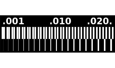 Callibration File
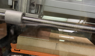 Mill Cutting Test File
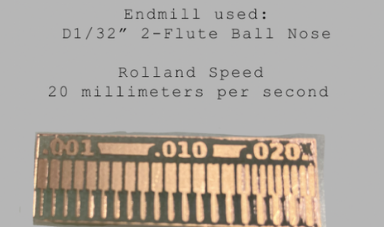 Callibration Cut Results
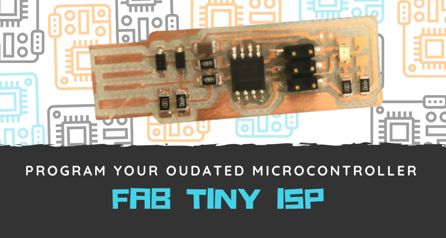
FabTiny ISP
An ISP or In sytem programmer is a tool that allows us to code the series 0 attiny. An in system programmer allows us to code microcontrollers after they have been mounted, and do not force us to code the board before assembly. This is extremely useful for debugging and convenience purposes. However we cannot simply plug in the board we make to the USB port on our computer since they do not speak the same protocol, so we make need to make a type of programmer that will translate the output of our USB and send it to the attiny, that is what the FabTINY ISP does. This tool was much more useful before, but now we have the series one attiny which can be programmed simply with an ftdi cable which will convert USB to serial, somehting far more convenient for us to use. So this project is now here as just a cool beginner project to follow even though we will never use this programmer.
Following the same procedure discussed above we milled our own FabTiny ISP using mods. To do this I got the PNG image that Fab Acadmey provided it, and put it into MODS. I set up the proper settings in MODS, got the RML file, brought it to the machine, set up the mill using V-Panel and ran the RML. I then used MODS again for the outline file, selected the 1/32 bit and outline mode, and repeated the same process from there with the RML file. This got me my milled out board.
Step by step the process we followed for mods and milling is as follows. First we went the mods website. Then we selected programs, open server module, and selected the roland SRM-20 with a png image. We then delete the node for websocket device. Then we opened module and got the server module for saving a file and linked it to the roland srm20 module which outputs a file. This will make it so that when the file is made it is not sent to the machine, but saved locally instead. We then made sure to set the origin settings to 0 for all values. We then clicked on select png, and uploaded our png file of the fab tiny isp. We then selected the mill traces tool (1/64), then calculate, which saves the file for us in downloads. We then repeat this process uploading our outline, and selecting mill outline (1/32), and click on calculate again. This produces RML files for both the outline and the traces.
Next up we go to the mill, and open on the computer connected to it V-Panel. V-Panel is the software that directly controls the mill, and lets us upload files. We go to setting make sure RML is selected as the file type, and select machine coordiantes as the coordiante mappings since the RML values from mods is in machine coordinates. Next I live the collet up, and insert my 1/32 ball nose endmill. I also attach the pcb to the spoilboard with double sided tape. I then bring it to the xy zero and zero it in vpanel. I then lower the endmill in vpanel till it is close to the pcb, then use the allen key to drop the endmill onto the PCB, and then tighten and set that as my zero value in Vpanel. I then upload the file, and click output to run it. I had to repeat this process nearly five times since each time the traces would be good in one area and too shallow in another, or too deep in one area and too shallow in another. This was infuriating I tried a variety of different methods to solve this from trying to zero the z axis in the middle of the work area, pushing down the pcb slightly when zeroing, changing the cut depth in mods, and nothing worked well until I found the perfect solution, buy my own Chinese mill from the interent for a fraction of the cost that can have a proper workdholding better than tape and can make a height map. Eventually I got to a board that worked out of sheer luck.
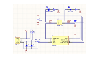 Fab Tiny Schematic
Fab Tiny Footprint
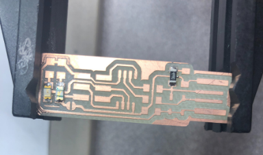
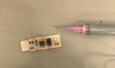
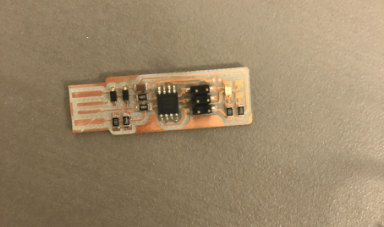
Fab Tiny Milled Board
Fab Tiny Schematic
Fab Tiny Footprint
Fab Tiny Milled Board
Soldering and Multimeter
The next step to this project is to solder the components onto the board. There are two types of components through hole and suface mounted. Surface mounted components are components that are attached on top of the board, while through hole components go through the board. For this project we will be using exclusively surface mounted components however it is possible to mix and math depending on your purpose (not with MODS though Mods cannnot mill through hole components) For this project I got the list of needed SMD components from Fab Academy ready which included some zener dioes, resistors, leds, an attiny45, and a pin header. To solder these components on the board we used solder paste. Solder paste is a mixture of solder and a high vapor pressure solvent which allows us to apply a bit of the solder paste to the pads, lay our component on top, and use a heat gun. The heat will evaporate the solvent leaving just the solder left, and since solder can ony bind to metals and has a high surface tension it will align the component for you perfectrly without any work needed to be done with precesions, without any solder binding to the substrate. Another method, but far more difficult especially with SMD components is using solder wire. Solder can only bind to heated copper, so to use solder wire effectively one first heats up the copper with a soldering iron, then while holding the iron against the copper, heats up the wire as well to melt the solder onto the copper pad. This technique is used to make the USB connections.
An Imporant tool when soldering is the multimeter, I used it constantly when soldering the board to make sure that all the compnents were connected properly. There are three main modes on a multimeter that matter to us for this project being the contiuity mode, which lets us make sure the traces are connected. Resistance mode which will tell the resistance of a components since you should not trust the boxes that everyone has access to. And the diode mode which is useful to know what orientation to put the diode since they have a polarity.
 Placing First Components
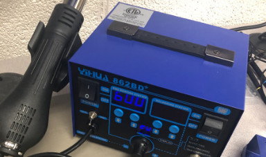 Soldering Station
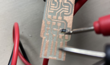 Testing Continuinity
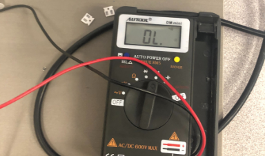 Multimeter
 Solder Paste
 Soldered Board
Programming the Board and Debugging
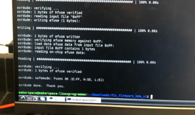
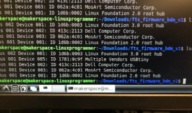
Finally all that's left ot do is program the board. To do this we download and compile AVRdude, which we can easily get on a linux machine using apt package manager. For this step is to build the package, since we are using the default settings there is no need to change anything and we just have to build it. Then we will connect my attinty to one that is already set up and use it to progam my board. I will then flash my attiny which will wipe it and rewrite it with the built hexfile. All that's then left to do is set the fuses by running the make fuses command which will set the clock and other internal set ups allowing the computer to recognize it as a USB device. It is then shown it works by typing lsub, and seeing it in the list of devices.
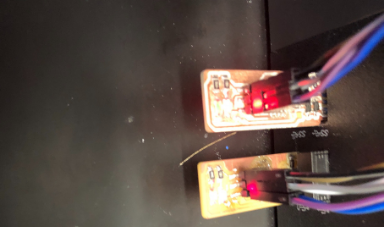
When doing this process, I did not run into many complications, the main one I ran into was just pour connection with the programmer which lead to me beleiving there were other problems that were not actually there. This then lead to to removing the diodes and flipping them backwards, not realzing I should have just made sure the wires were well connected.
To do this process first thing to do is use apt to instal avr dude which will allow us to upload files to avr products. Then we need to download the firmware source code form the Fab Academy website that will go on our attiny, and run the make file which will compile it. This will build a hex file that can go onto our attiny. The next step is to edit the make file with nano and make sure that the programmer is set to another ATtiny by inputting the line usbtiny next to programmer in the make file. We then connect our attiny to the attiny programmer appropriately, and plug them both into the computer. This is when the red led lit up on my board indicating it was done properly. First make flash is run which flashes the memory of my ISP, and clears it. Then we run the make fuses command to set the clock of my attiny and let it be read as a general usb key to the computer by having the computer dictate its clock speed. This can then be confirmed with lsusb now displaying my attiny in the list. It is possible at this point to change the name of my attiny to have its own unique USB id, but I chose not to. This confirms everything is working, and the attiny is working and can communicate with the computer. We then run the rsrdisbl command which does the same thing is the previous command, but sets all fuses including the reset pin meaning that we cnanot communicate to the board again though AVRdude. All thats left is to remove the jumper made with solder, and my FabTIny ISP can now program other boards.
Finally all that's left ot do is program the board. To do this we download and compile AVRdude, which we can easily get on a linux machine using apt package manager. For this step is to build the package, since we are using the default settings there is no need to change anything and we just have to build it. Then we will connect my attinty to one that is already set up and use it to progam my board. I will then flash my attiny which will wipe it and rewrite it with the built hexfile. All that's then left to do is set the fuses by running the make fuses command which will set the clock and other internal set ups allowing the computer to recognize it as a USB device. It is then shown it works by typing lsub, and seeing it in the list of devices.
When doing this process, I did not run into many complications, the main one I ran into was just pour connection with the programmer which lead to me beleiving there were other problems that were not actually there. This then lead to to removing the diodes and flipping them backwards, not realzing I should have just made sure the wires were well connected.
To do this process first thing to do is use apt to instal avr dude which will allow us to upload files to avr products. Then we need to download the firmware source code form the Fab Academy website that will go on our attiny, and run the make file which will compile it. This will build a hex file that can go onto our attiny. The next step is to edit the make file with nano and make sure that the programmer is set to another ATtiny by inputting the line usbtiny next to programmer in the make file. We then connect our attiny to the attiny programmer appropriately, and plug them both into the computer. This is when the red led lit up on my board indicating it was done properly. First make flash is run which flashes the memory of my ISP, and clears it. Then we run the make fuses command to set the clock of my attiny and let it be read as a general usb key to the computer by having the computer dictate its clock speed. This can then be confirmed with lsusb now displaying my attiny in the list. It is possible at this point to change the name of my attiny to have its own unique USB id, but I chose not to. This confirms everything is working, and the attiny is working and can communicate with the computer. We then run the rsrdisbl command which does the same thing is the previous command, but sets all fuses including the reset pin meaning that we cnanot communicate to the board again though AVRdude. All thats left is to remove the jumper made with solder, and my FabTIny ISP can now program other boards.
 Programming the Board
 Running Make Fuse
 Board appearing in lsusb
Click Here to Download all the files from these projects!