Week twelth assignment is the output devices.This week Neil has introduced as about different output devices.How we calculate the power of output device and its need.Program the MCU for controlling the output device.
Hero video.
Assignment-12
Output Devices
OBJECTIVES
Group assignment
- Measure the power consumption of an output device
- Document your work (in a group or individually)
Individual assignments
- Add an output device to a microcontroller board you've designed and program it to do something.
Learning outcomes
- Demonstrate workflows used in controlling an output device(s) with MCU board you have designed.
About Group Assignment
Task for the group assignment is to calculate the power of output devices.I have used the Hxahust fan and 12 volt (DC) submersible water pump.so for the group assignment I tried to calculate the power of these two devices.
Input refers to the amount of energy put into a device, and outputrefers to the amount of energy that comes out. A
a device may change the type of energy but not the amount. For example, a light bulb’s input energy is the form of
electrical energy, and its output energy is in the form of light and heat.
Power
Power, measured in watts, is the rate at which a device converts energy. Power is dependent on the current rating of an appliance and the voltage passing through it. Power is calculated using the following equation.
power (watts) = current rating (amps) × voltage (volts)
P = I × V
Calculating Power for AC Exahust Fan
I have used the multimeter for measureing the AC current and AC voltage required for the exahust fan as shown in images
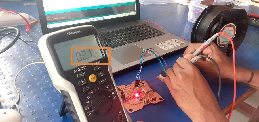
Measuring AC Current
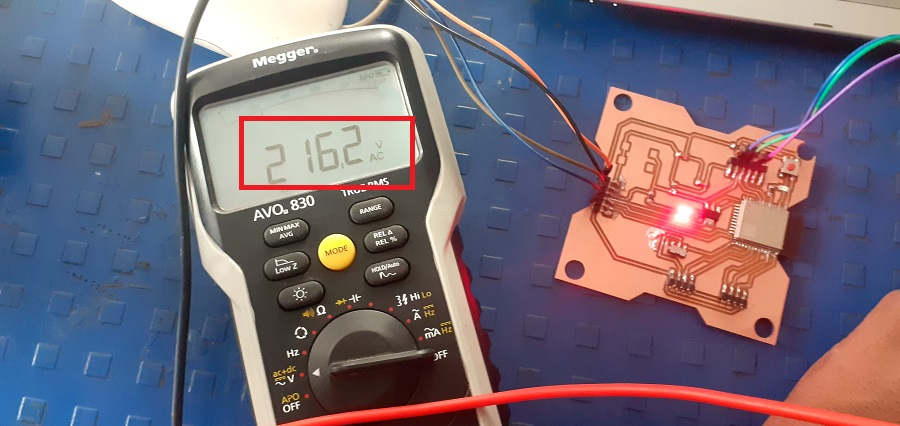 Measuring AC voltage
Current(I)=0.21mA, Voltage(V)=216.2 Volt
Power(P)=0.21 x10x216.2
Power(P)=0.045 W
Calculating Power for 12VDC submersible water pump.
The power of water can be calculate in two ways in presence of air and in presence of water.
In presence of air
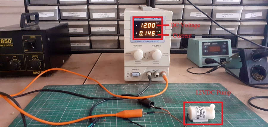
In presence of air
Current(I)=0.146 A, Voltage(V)=12 Volt
Power(P)=0.146x12
Power(P)=1.752 W
In presence of water
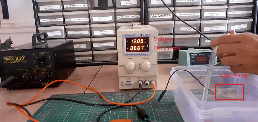
In presence of water
Current(I)=0.667 A, Voltage(V)=12 Volt
Power(P)=0.667x12
Power(P)=8.004 W
Individual assignment on Output Devices
In this assignment we have to uesd any ouput device connected it with self design MCU and and program it to do something.In my final project I used AC exahust fan and 12volt DC submersible water pump as output device.I have design ESP32 board in Input devices assignment,tried to program it for given output devices, started with the same.The work flow of the assignment is given below.
- About Output devices
- AC Exahust Fan.
- 12volt DC submersible water pump.
- About Transistor.
- About Relay.
- Switching Circuit.
About Output devices
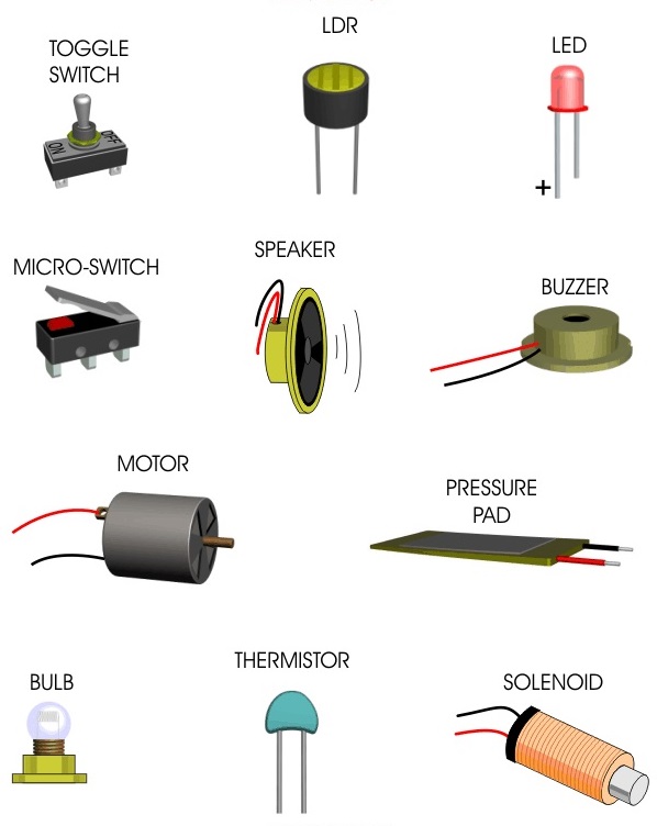
An ouput device is define as the device which convert Electrical energy in to other form of energy,called as Output device.There are different output devices like LED, AC and DC motor,Speaker etc.
AC Exahust Fan.
In my project I used the AC exahust fan for cooling purpose,the specification of AC exahust fan is given below.
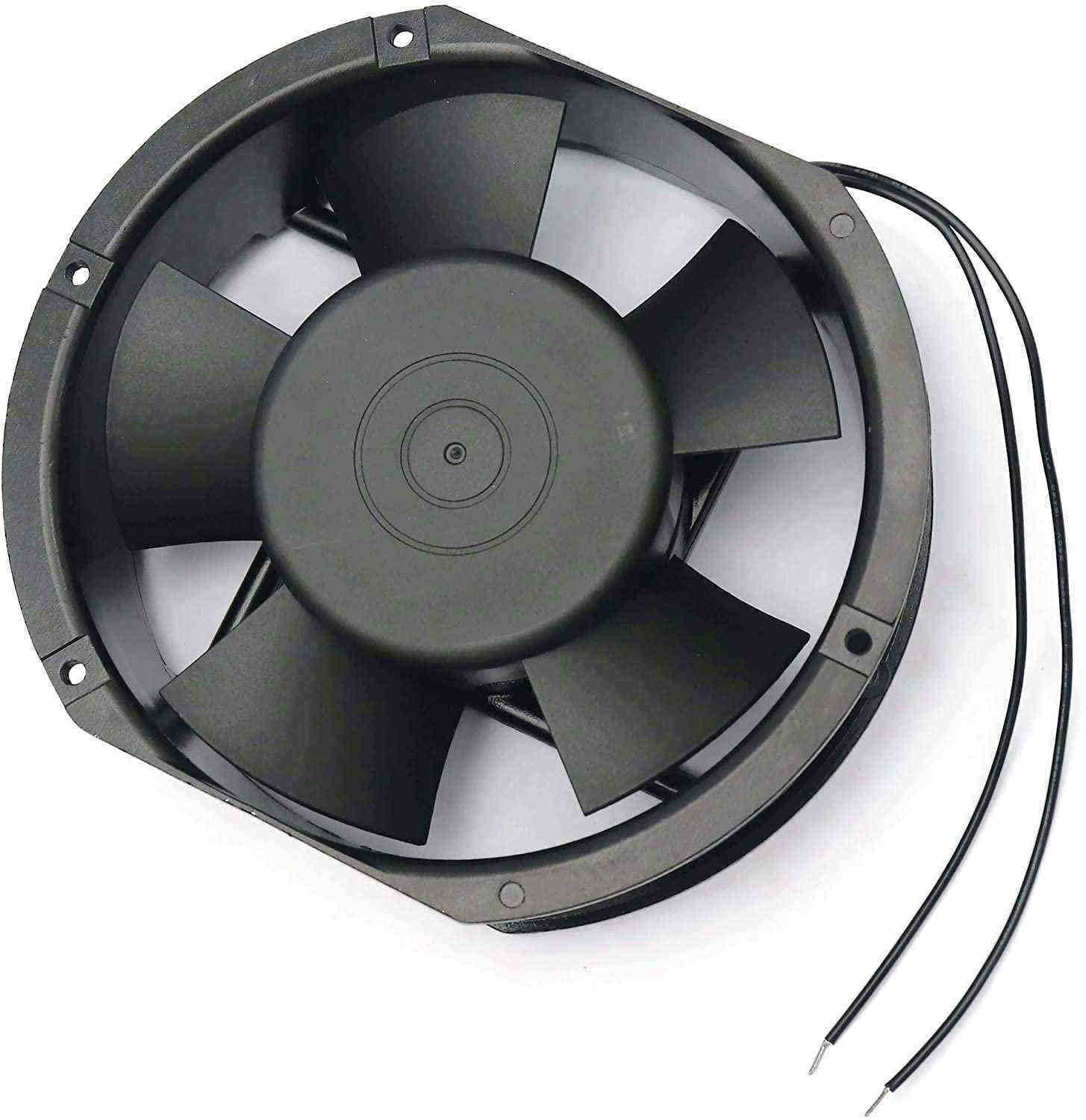
- Model name - 17250 (oval shape) 6 Inch
- 220-240V ~ 50/60 Hz
- Current :0.22A
- Power :37W
- Impedence Protected
The specification of AC Exahust fan
12volt DC submersible water pump.
For pumping the water on fan pad I have used the DC 12 volt Submersible water pump, the specification of water pump is given below
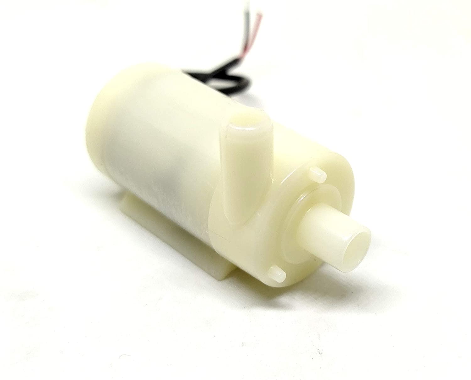
- It can take up to 120 L per hour with very low current consumption of 220mA.
- Voltage: 3V - 12V
- Flow rate: 80-120L/H
- Maximum lift: 40-110cm
- Nozzle Diameter: 7.5mm
- Length: 8mm
- Diameter: Approx. 23mm, Length: Approx. 53mm, Height: Approx. 32mm
- Just connect tube pipe to the motor outlet, submerge it in water and power it. Make sure that the water level is always higher than the motor
- It can work in submersible and non submersible condition as it has a nozzle at input and output both do an pipe can be attached at input also.
The specification of 12VDC Pump
About Transistor.
A transistor is a semiconductor device used to amplify or switch electronic signals and electrical power. Transistors are one of the basic building blocks of modern electronics. It is composed of semiconductor material usually with at least three terminals for connection to an external circuit. A voltage or current applied to one pair of the transistor's terminals controls the current through another pair of terminals. Because the controlled (output) power can be higher than the controlling (input) power, a transistor can amplify a signal.
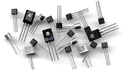
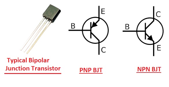
Parts of a Transistor
A typical transistor is composed of three layers of semiconductor materials or more specifically terminals which helps to make a connection to an external circuit and carry the current. A voltage or current that is applied to anyone pair of the terminals of a transistor controls the current through the other pair of terminals. There are three terminals for a transistor. They are;
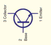
- Base: This is used to activate the transistor.
- Collector: It is the positive lead of the transistor.
- Emitter: It is the negative lead of the transistor.
Transistor Symbol
A diagrammatic form of n-p-n and p-n-p transistor is exposed. In-circuit is a connection drawn form is used. The arrow symbol defined the emitter current. In the n-p-n connection, we identify electrons flow into the emitter. This means that the conservative current flows out of the emitter as indicated by the outgoing arrow. Equally, it can be seen that for the p-n-p connection, the conservative current flows into the emitter as exposed by the inward arrow in the figure.
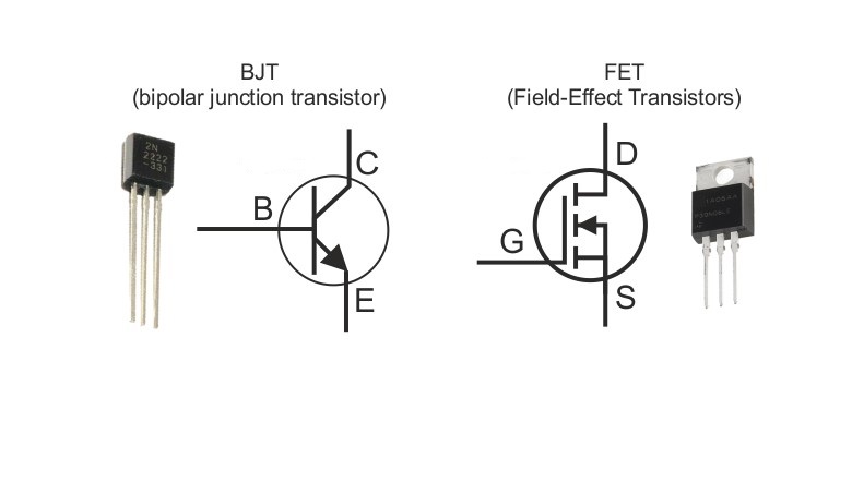
Types of transistor
Mainly we can divide the Transistor in two categories Bipolar Junction Transistor (BJT) and Field Effect Transistor (FET).
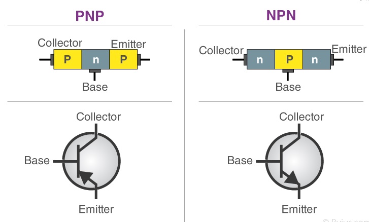
Bipolar Junction Transistor (BJT)
Bipolar Junction Transistors are transistors that are built up of 3 regions, the base, the collector, and the emitter. Bipolar Junction transistors, different FET transistors, are current-controlled devices. A small current entering the base region of the transistor causes a much larger current flow from the emitter to the collector region. Bipolar junction transistors come in two major types, NPN and PNP. An NPN transistor is one in which the majority of the current carriers are electrons. Electron flowing from the emitter to the collector forms the base of the majority of current flow through the transistor. The further types of charge, holes, are a minority. PNP transistors are the opposite. In PNP transistors, the majority of current carrier holes. BJT transistors are available in two types namely PNP and NPN.
Advantages of Transistor
- Lower cost and smaller in size.
- Smaller mechanical sensitivity.
- Low operating voltage.
- Extremely long life.
- No power consumption.
- Fast switching.
- Better efficiency circuits can be developed.
- Used to develop a single integrated circuit.
Limitations of Transistors
- Transistors lack higher electron mobility.
- Transistors can be easily damaged when electrical and thermal events arise. For example, electrostatic discharge in handling.
- Transistors are affected by cosmic rays and radiation.
Transistors also have few limitations. They are as follows;
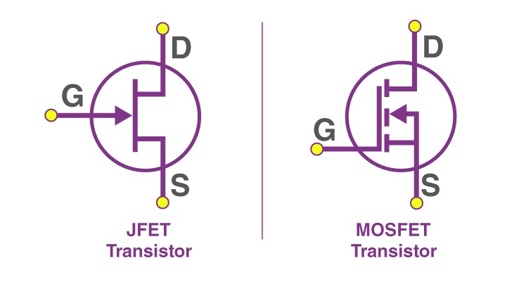
Field Effect Transistor (FET)
Field Effect Transistor contains the three regions such as a source, a gate, a drain. They are termed as voltage controlled devices as they control the level of voltage. To control the electrical behavior, the externally applied electric field can be chosen that’s why called as field effect transistors. In this, current flows due to majority charge carriers i.e., electrons, hence also known as the uni-polar transistor. It has mainly high input impedance in mega ohms with low frequency conductivity between drain and source controlled by electric field. FETs are highly efficient, vigorous & lesser in cost.Field effect transistors are of two types i.e., Junction field effect transistors (JFET) and Metal oxide field effect transistors (MOSFET).The current passes between the two channels named as n-channel and p-channel.
Metal Oxide Semiconductor Field Effect Transistor(MOSFET)
Metal Oxide Silicon Field Effect Transistor is abbreviated as MOSFET. It is merely a unipolar transistor and used as an electronic switch and to amplify electronic signals. The device has three terminals consisting of a source, gate and drain. Apart from these terminals there is a substrate generally called the body which is always connected to the source terminal for practical applications. In recent years, its discovery has led to the dominant usage of these devices in digital integrated circuits due to its structure. The Silicon di-oxide (SiO2) layer acts as an insulator and provides electrical isolation between the gate and an active channel between the source and the drain which provides high input impedance which is almost infinite thus capturing all the input signal.
Working principle of MOSFET
It is fabricated by the oxidation of silicon substrates. It works by altering the width of the channel through which the movement of charge carriers (electrons for N-channel and holes for P-channel) occurs from source to drain. The gate terminal is insulated whose voltage regulates the conductivity of the device.
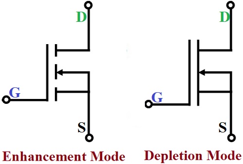
Types of MOSFET
On the basis of Operational Mode, MOSFETs can be classified into two types.
- Enhancement Type MOSFETs
- Depletion Type MOSFETs
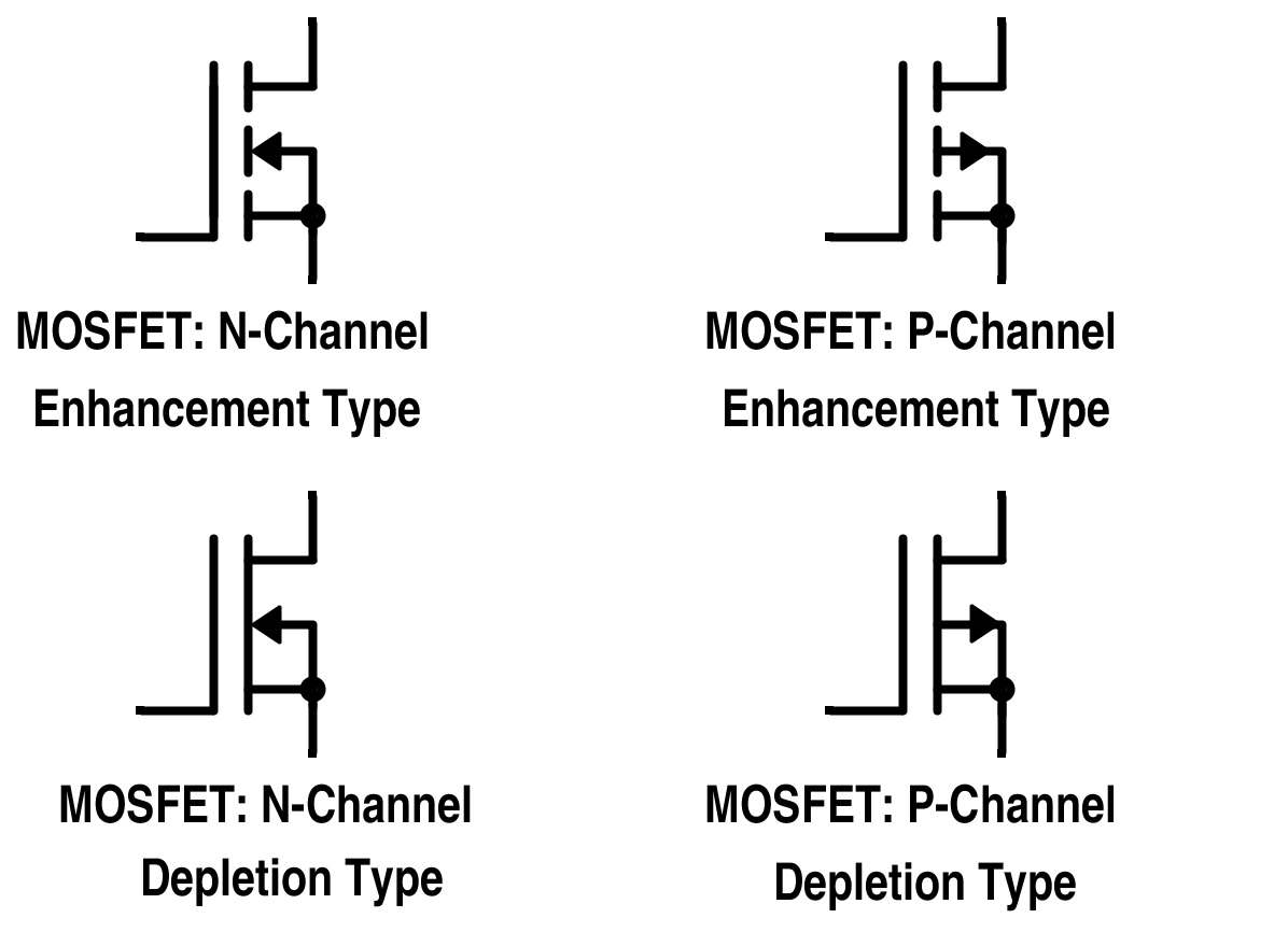
Citcuit Symbol of Different MOSFET
About N Channel Enhancement Type MOSFET
In this mode, there is no conduction at zero voltage which implies it is closed or “OFF” by default as there is no existing channel. When the gate voltage is increased more than the source voltage, the charge carriers (holes) shifts away leaving behind the electrons and thus a wider channel is established.The gate voltage is directly proportional to the current i.e. as the gate voltage increases the current increases and vice versa.In my switching circuit I have used N channel.
- A lightly doped P-type substrate forms the body of the device and the source and drain are heavily doped with N-type impurities.
- N-channel have electrons as majority carriers.
- The applied gate voltage is positive to turn “ON” the device.
- It has lower inherent capacitance and smaller junction areas due to the high mobility of electrons which makes it to operate at high switching speeds.
- It contains positively charged contaminants which makes the N-channel MOSFETs to turn on prematurely.
- Drain resistance is low compared to P-type.
Specially about N Channel Enhancement Type MOSFET
Applications of MOSFET
- MOSFET amplifiers are extensively used in radio frequency applications.
- It acts as a passive element like resistor, capacitor and inductor.
- DC motors can be regulated by power MOSFETs.
- High switching speed of MOSFETs make it an ideal choice in designing chopper circuits
Advantages of MOSFET
- MOSFETs provide greater efficiency while operating at lower voltages.
- Absence of gate current results in high input impedance producing high switching speed.
- They operate at lower power and draws no current.
Disadvantages of MOSFET
- The thin oxide layer make the MOSFETs vulnerable to permanent damage when evoked by electrostatic charges.
- Overload voltages makes it unstable.
MOSFET also have few limitations. They are as follows;
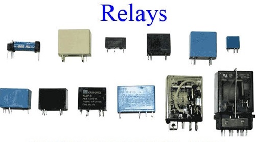
About Relay
Converting a small electrical input into a high-current output is no easy feat, but this task is necessary to efficiently operate a wide range of standard appliances and vehicles. Many circuits achieve these conversions through the use of relays, which are indispensable in all kinds of electronic equipment.Relays are electric switches that use electromagnetism to convert small electrical stimuli into larger currents.These conversions occur when electrical inputs activate electromagnets to either form or break existing circuits.By leveraging weak inputs to power stronger currents, relays effectively act as either a switch or an amplifier for the electric circuit, depending on the desired application.
Applications of Relay
- They are used in electronic circuits and home appliances for isolating low voltage or DC circuits from high voltage AC circuits.
- They are the backbone of industrial process automation systems.
- They are used in combination with PLCs for process control.
- They are one of the key components in an automation cabinet
- Used for signalling and control in railway networks.
- In motor control circuits for motor switching, protection as well as control.
- In substations and power distribution centers for sensing various faults and operating the circuit breaker.
Relays have a wide range of applications starting from washing machines at homes to the telecommunication systems at the International space station, they can be found everywhere. The following are a few key applications:
How Does a Relay Work?
Relays differ in their size, capacity, and corresponding uses. However, although they may differ in these respects, all relays function in essentially the same way: one circuit is used to power another. The specific manner in which this occurs depends on whether the relay is normally open (NO) or normally closed (NC).
Normally Open Relays
Most relays are normally open; that is, the second, larger circuit is in the off position by default. In a normally open relay, power flows through an input circuit, activating an electromagnet. This generates a magnetic field that attracts a contact to join with the second, larger circuit, allowing current to flow through. When the source of power is removed, a spring draws the contact away from the second circuit, stopping the flow of electricity and turning off the end device.
Normally Closed Relays
The fundamentals of an NC relay are the same as an NO relay: there are two circuits, with the second being larger, and an electromagnet moves a physical contact between two positions. But in the case of an NC relay, the default states are reversed. When the first circuit is activated, the electromagnet draws the contact away from the second circuit. As such, NC relays keep the larger circuit in the on position by default.
About BC547 Transistor
The BC547 transistor is an NPN transistor. A transistor is nothing but the transfer of resistance which is used for amplifying the current. A small current of the base terminal of this transistor will control the large current of emitter and base terminals. The main function of this transistor is to amplify as well as switching purposes. The maximum gain current of this transistor is 800A.For more details click on BC547 Data-sheet.
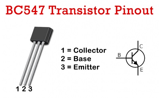
Pin out of BC547
- 1-Collector:Current flows in through collector
- 2-Base:Controls the biasing of transistor
- 3-Emitter:Current Drains out through emitter
The Pin Configuration is as follows
Features of BC547
- The gain of DC current (hFE) = 800 A
- Continuous Ic (collector current) = 100mA
- VBE (emitter-base voltage) = 6V
- IB (base current) = 5mA
- The polarity of the transistor is NPN
- The transition frequency is 300MHz
- It is obtainable in semiconductor package like-92
- Power dissipation is 625mW
The features of the BC547 transistor include the following.
Applications of BC547
- Driver Modules like Relay Driver, LED driver etc..
- Amplifier modules like Audio amplifiers, signal Amplifier etc..
- Darlington pair
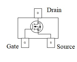
About N-Channel Logic Level Enhancement Mode Field Effect Transistor(NDS355AN)
SuperSOT™-3 N-Channel logic level enhancement mode power field effect transistors are produced using ON Semiconductor's proprietary, high cell density, DMOS technology. This very high density process is especially tailored to minimize on-state resistance. These devices are particularly suited for low voltage applications in notebook computers, portable phones, PCMCIA cards, and other battery powered circuits where fast switching, and low in-line power loss are needed in a very small outline surface mount package.For more details click on NDS355AN Data-sheet.
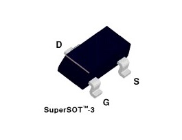
Pin out of NDS355AN
Features of NDS355AN
- 1.7 A, 30 V. RDS(ON) = 0.125Ω @ VGS= 4.5 V
- RDS(ON) = 0.085 Ω @ VGS= 10 V
- Industry standard outline SOT-23 surface mount package using poprietary SuperSOT™-3 design for superior thermal and electrical capabilities
- High density cell design for extremely low RDS(ON)
- Exceptional on-resistance and maximum DC current capability
- Compact industry standard SOT-23 surface mount package
The features of N-Channel Logic Level Enhancement Mode Field Effect Transistor(NDS355AN) include the following.
About Relay(YL303H-S-5VDC-1Z)
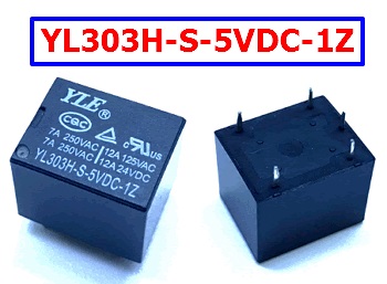
- Function : 5V DC, PCB Relay
- Package : 5Pin PCB Type
- Manufacturers : YLE
- For more details click on Data-sheet.
Pin out
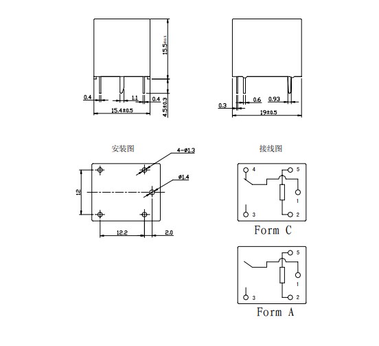
Features
- 10A switching capability
- Small footprint
- Sealed type available
- Class B/F available
- ConformtoRoHS,ELV directive
Description
- Size (mm) : 19.2 x 15.5 x 15.5
- Coil Voltage (VDC) : 5
- Contact Material : Sliver Alloy
- Changeover contact : 10A
Characteristics Data
- Insulation Resistance : 100MΩMin at 500VDC
- Dielectric Strength Between Open Contacts : 750VAC(50/60Hz for one minute)
- Between Contacts and coil : 1500VAC(50/60Hz for one minute)
- Operate Time : 10ms
- Release Time : 5m
Contact load
- 10A/125VAC
- 10A/28VDC
- 7A/240VAC
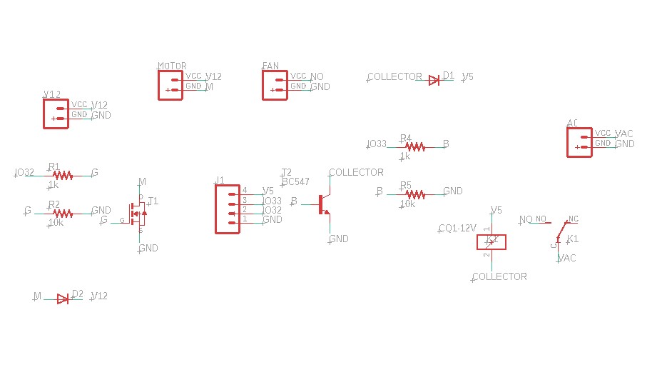
Design Switching Circuit
Schematic of Switching Circuit In Eagle
In this assignment I have AC exahust fan and 12VDC motor pump as output device.For operating the AC exahust fan I have used the Relay as switch where as for 12VDC pump used MOSFET as switch.The Schenatic for switching CKT is given below.
Schemtic of Switching Circuit
Switching Circuit Board
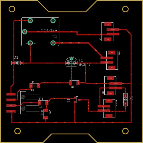
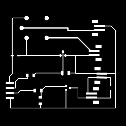
Switching Circuit Trace
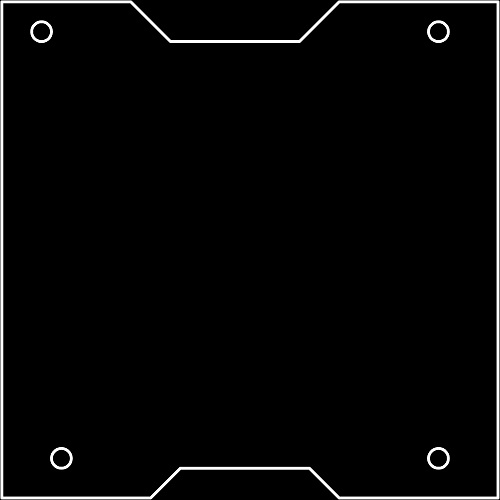
Switching Circuit cutout
Milling,Stuffing and Soldering

Milling the Switching Board.
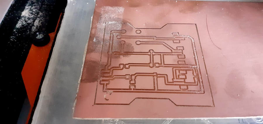
Milled Switching Board.
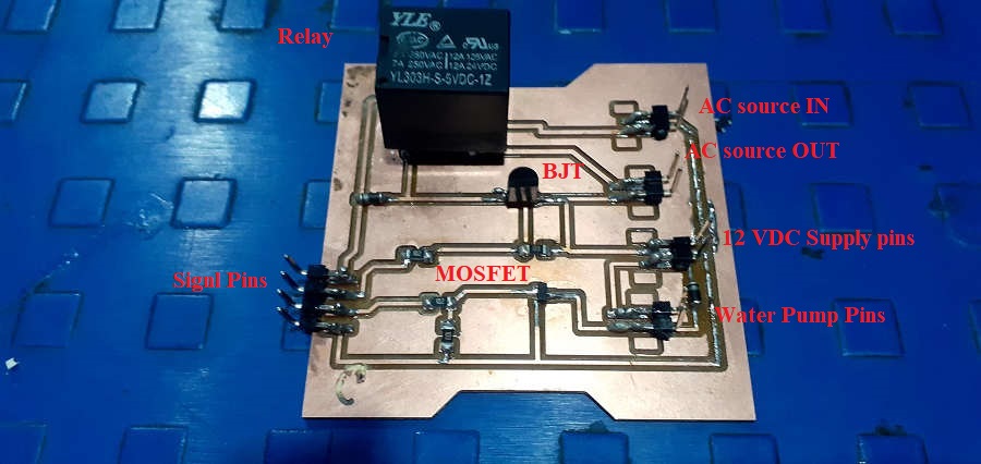
Stuffed and Soldered Switching circuit board.
Interfacing Microcontroller with Output Devices
Interfacing AC Exahust Fan with ESP32 Through Relay.
Interfacing AC exahust fan with ESP32 board is as shown below.
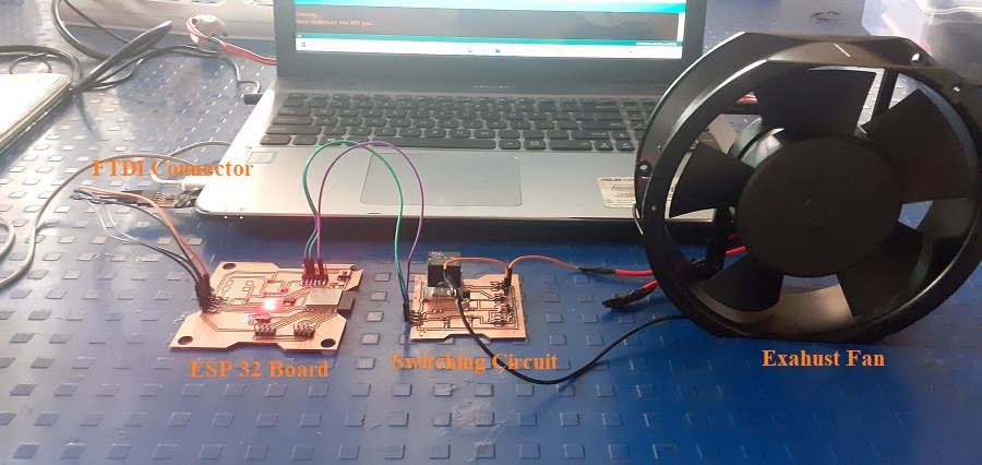
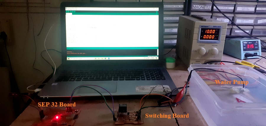
Interfacing 12VDC Submesuresible water Pump with ESP 32.
Interfacing of 12VDC water pump with ESP32 board is as shown below.
Programming of ESP32 Microcontroller.
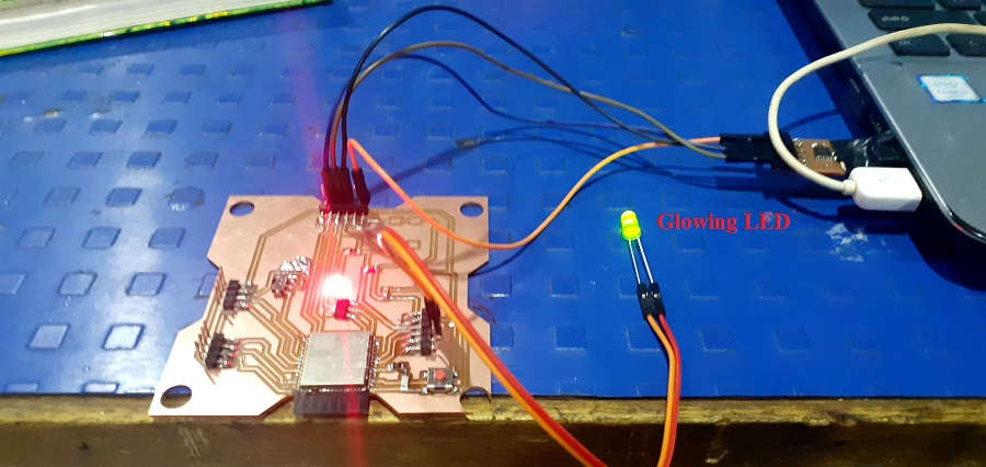
Blinking of LED
Initially I tried the output device LED.For this I have consider the simple LED blinking code.In this program I Consider the IO32 pin as output pin and run the code.The program code is given in the image.
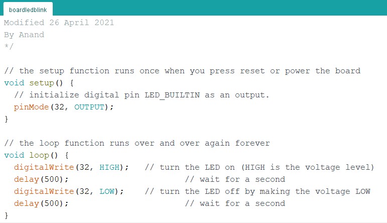
The LED will glow and blink as shown in the image.
AC Exahust Fan
In this programming code I have consider the IO33 pin as output pin.Initially the pin is made high so the relay get 3.3 volt get switch on.The AC exhaust fan on for 2 second as delay is 2000.Now the pin made low, relay does get any input, it get off.The exahust fan get stop, the process get continue.The program code is given in the image.
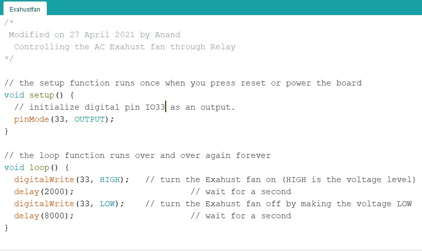
The exahust fan is on and off shown in video
12VDC submersible water pump
In this programming code I have consider the IO32 pin as output pin.Initially the pin is made high so the gate of MOSFET get 3.3 volt and switch on.The water pump on for seconds.Now the pin made low, the gate voltage becomes lower than threshold voltage thus does get any input, it get off.The pump get stop, the process get continue.The program code is given in the image.

The water pump is on and off shown in video
Learning Outcomes
- I introdued with different output devices.
- I identified the features and specification of out put devices I have used.
- I measured curent and voltage of uesd output device and find its power.
- Designed, milled and stuffed the switching circuit.
- First time I used Relay,MOSFET and operate it using microcontroller.
- Program the microcrotroller for switching output devices.
Downloads
SAMS-Smart Azolla Multiplier System by Anand S. Tale is licensed under CC BY-SA 4.0![]()
![]()
![]()