Electronics Production
week 4 group assignment is to characterize the design rules for my PCB production process
Overview
This week we are going to explore about the Electronics Production which helps us to convert ideas to real world Products especially hardware. So it is necessary today if we want to control anything smart it required a smart hardware which perform well.There are many type of electronics production techniques available depends of the scale of the product
Basic electronics production steps:-
- Design the Idea to a Schematic
- Create PCB Layouts from the Schematic
- Make PCB (Printed Circuit boards) from the Layout
- Assemble the components on the PCB using Soldering
- Testing and Finishing
basic Electronics production steps are given above. So we are gonna learn and do how Electronics Productions are done in FAB lAB and which methods are using
For this assignment the Design and Layouts are already given so we don't have to make a design one.Instructed to make a In 'circuit Programer' as Individual assignment.The PCB production method I know is the chemical etching method but FAB Foundation not supports that method much because of the safety issues. So in FAB LABs We relay PCB Milling method for creating Prototyping PCBs
Milling machine
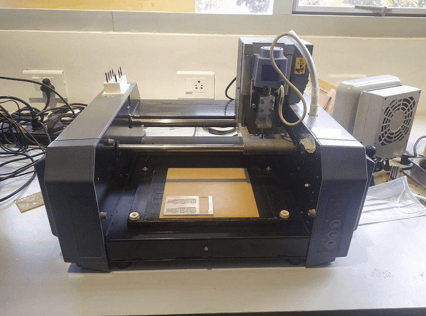
For PCB Production we use the milling machining method in fab labs which lets a person to make a PCB prototype like printing on paper using a paper printer so for PCB milling the FAB LAb provides a roland MDX 20 3 axis milling Machine.its a normal milling machine which we can also use for making PCBs
all three x,y and Z axis are driven by computer controlled stepper motor based on a live coordinate program called G-code,which will be send using the FAB Modes
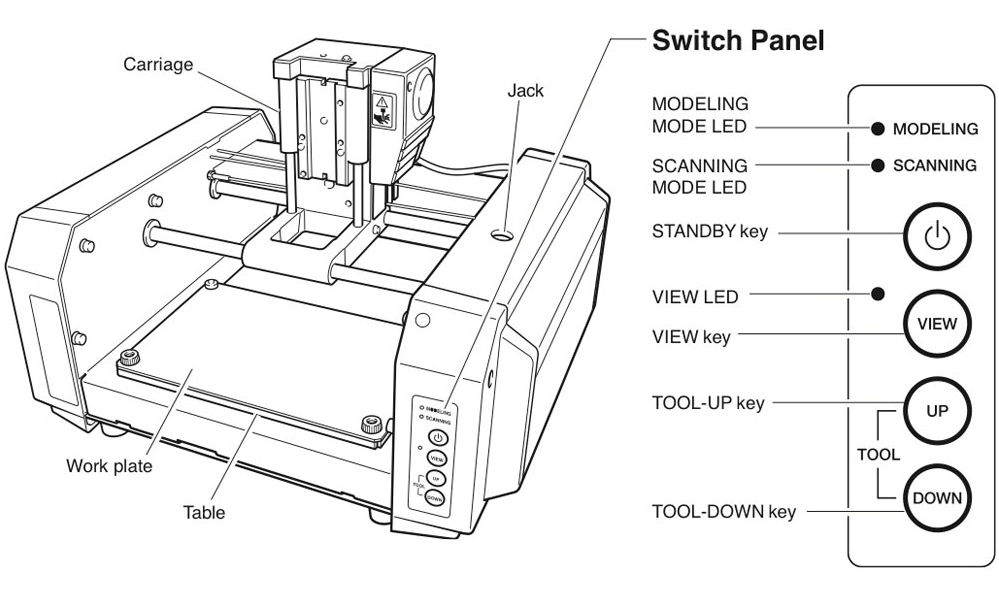
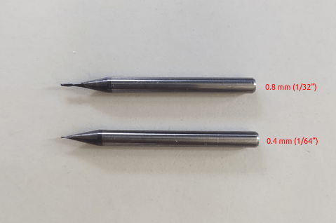
To start milling we should learn about the bed leveling and the cutting bits.in the machine manly uses 2 type of drill bits one is 0.4 mm(1/64") trace cutting bit other is 0.8 mm (1/32") pcb cutting bit
Milling Softwares
Of course in order to run the machine we need a User inter face or executing software. The software which Roland provides along with this milling machine is not focused on PCB milling also this machine isn't focused on PCB milling.And the software was made for windows operating system.So in the fab Foundation 2 different methods are supported this machine for PCB milling
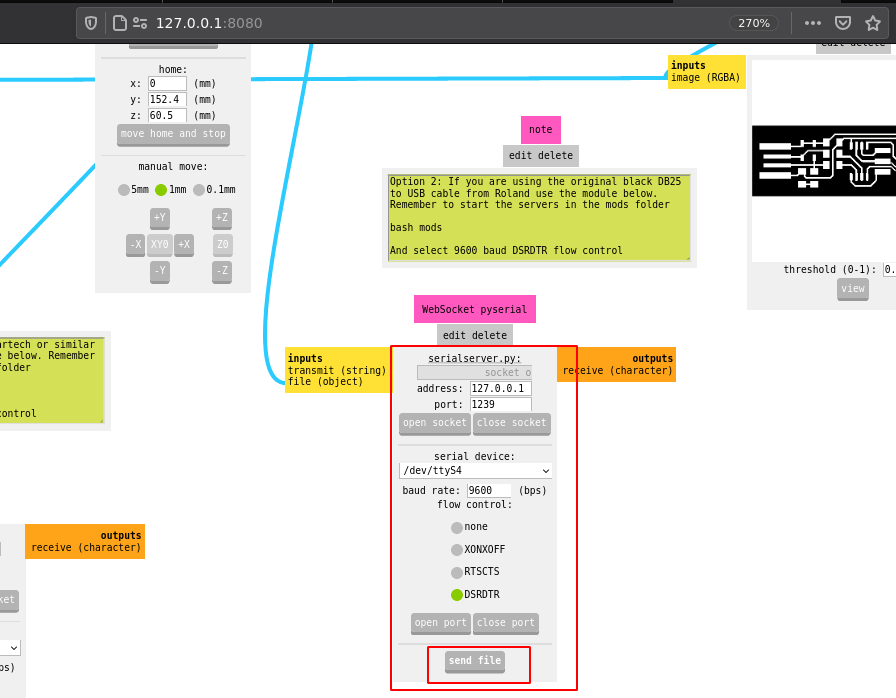
In MDX 20 fab tutorial method telling to use the FAB mods online for the slicing then it will convert to the machine instructions code which called G-code then that will send to machine using a g code executer interface software. Click here to see the Roland MDX 20 FAb tutorial
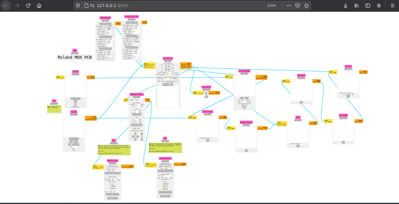
The new version of the FAB mods (offline) is the other method that all recommended because it doesn't need two software we can do all in the mods web app. And I already installed the FAB MODS in my Pc for the roland's vinal cutter during the Computer Controlled Cutting week. Check out my week3 documentation for the installation of FAB mods. The program can get in FAB mods by following:- Right click >> Programs >> Open programs >>
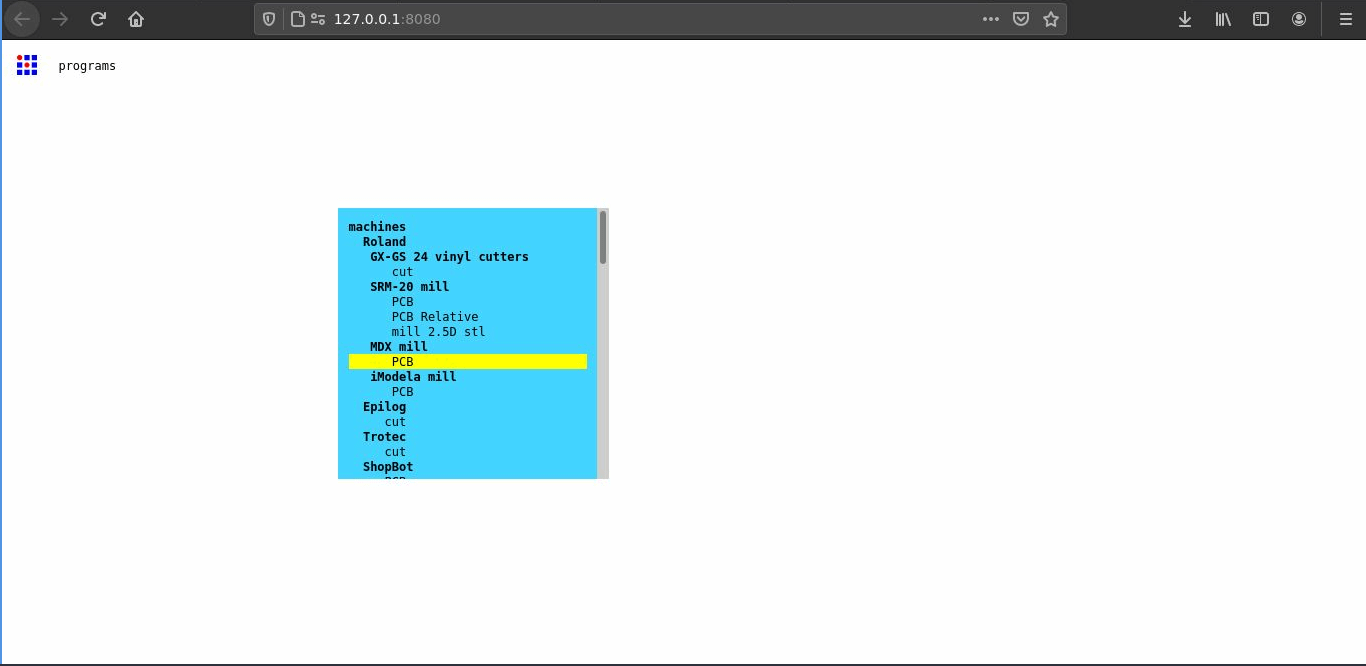
And click on the PCB option under the MDX mill
Resolution Test
After familiarization of the Milling machine we all did the group assignment as told. We tested the design rules which means here the resolution of the milling machine that tis how small it can mill out and cut .etc..
So the test is all about finding the thinnest PCB trace that can be milled out from the MDX 20 milling machine
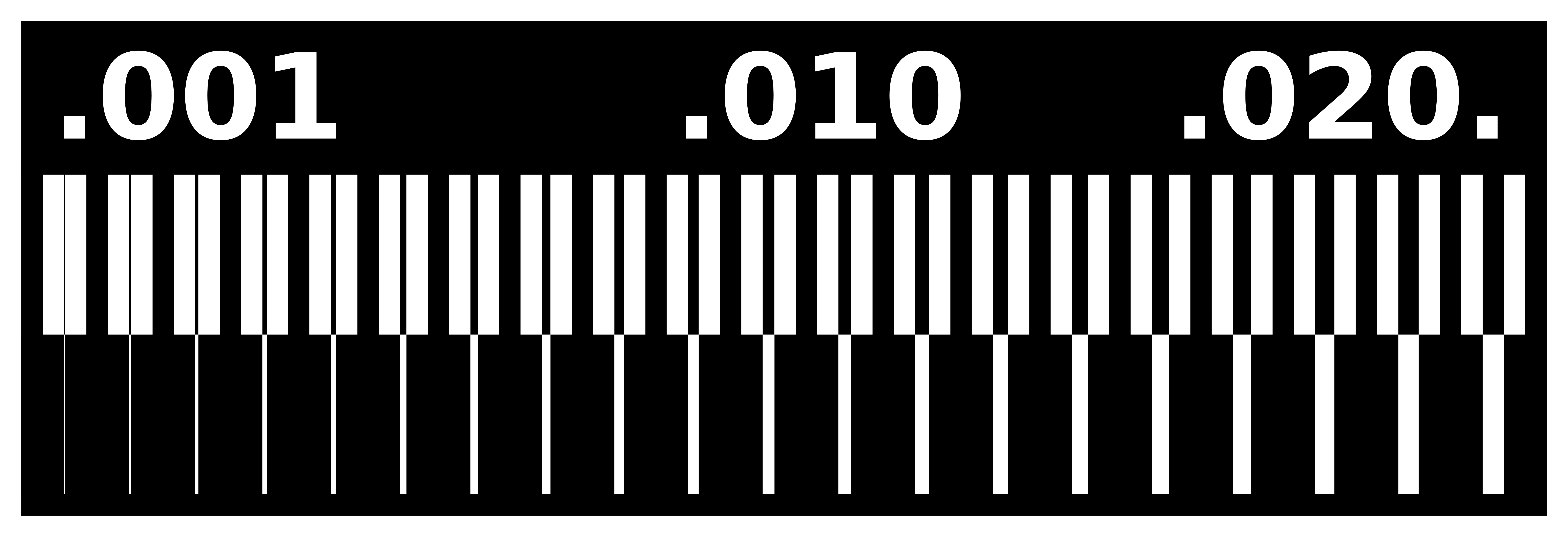
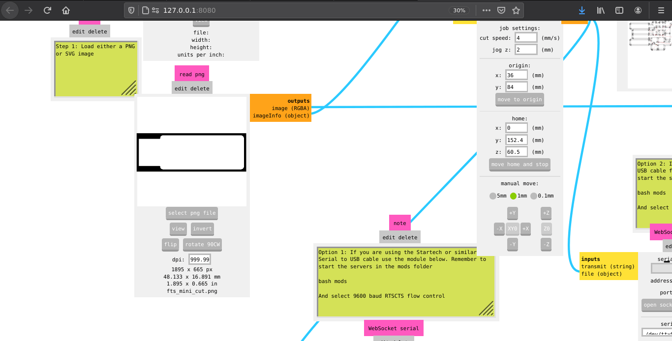
This is the line test PCB design provided by FAB foundation.So we loaded the png trace file to the FAB mods
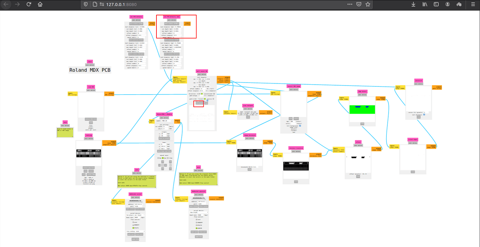
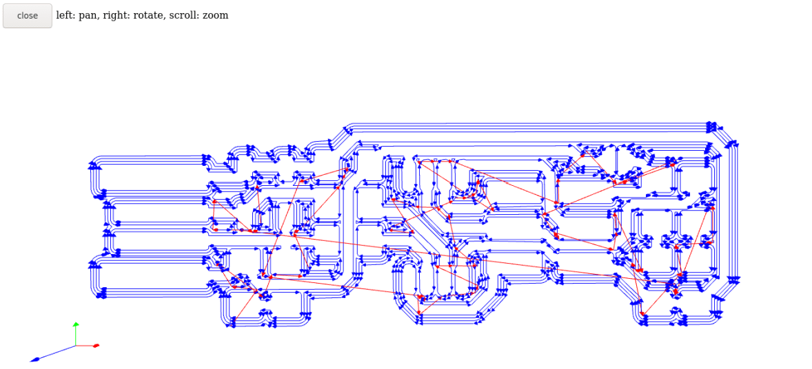
Then we calculated the tool path in fab mods for the 0.4 mm (1/64") Flat end mill. Then it opened a new window to view the generated tool path
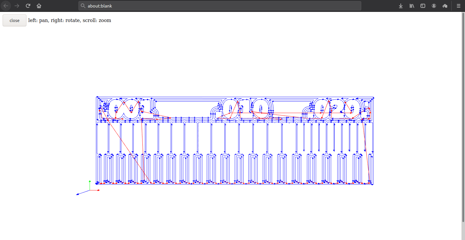
we can almost see the routing path of the tool that mend to be pass to cut the traces in the Blue highlighted lines.
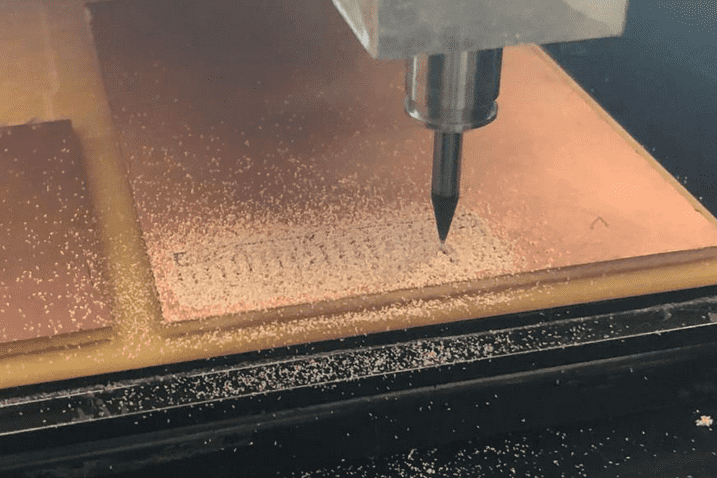
Then we milled out the lintest traces using 0.4 mm (1/64") flat endmill with the roland MDX 20 milling machine.The fab instructors help us out for the safety and user instructions
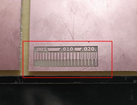
The results look promising after the trace milling we cut out the out line

The outline is also provided with the linetest files,but we need to change the tool into the cutting endmill
Then loaded the lintest.interior.png file to the FAB mods and changed the tool selection to cutting then calculated the tool path
After that we send the tool path to the machine in the fab mods then it started to cut out the outline
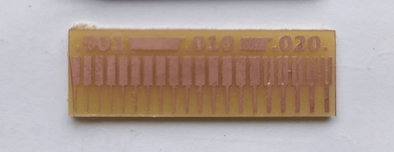
The final result of the finished PCB fore the line test look like this. So the test shows that we can get shortest traces upto 0.001 (1/1000") inches or 0.0254 mm with the (1/64") 0.4mm FLat endmill and proper calibration
For the comparison we also did another test with the 0.8 mm (1/32") Flat Endmill . The picture shows the different it wasn't necessary we are not gonna mill PCBs with 0.8 mm Flat Endmill any way
Summery :-
From the group assignment we understand the PCB design rules for the future as well as the Production method and using of the machine,software etc..
-
Design rules
- it possible to get thinnest trace which has width of 0.0254 mm or (1/1000") 0.001 inches but not oky to carry power in circuits.possible to burn when too much power pass through. Best suggestion is to keep the trace width of 0.010 or 0.254 mm for a better milling results.
- The Endmill we are using is a 0.4 mm (1/64") 2 Flute Flat endmill.So Its better to keep a distance of o.4 mm in between the traces or It not gonna mill out the space which is smaller than the 0.4 mm (1/64" :- 0.016)
- We can design any type of curve shaped PCB, what ever it is its possible to cut out in the milling machine
- designing single sided PCB's with surface mounded components (SMD type) if possible.It is the better option to save time and reduce the complexity
Click here For fiber laser engraved PCB line test results
week 4 assignment is to make an in-circuit programmer by milling and stuffing the PCB, test it, then optionally try other PCB processes
In-Circuit Programmer
to understand what is an in-circuit programmer is, You need to know about Microcontrollers.Nowadays electronics are mainly based on microcontrollers and microprocessors its like mini computer which has limited ram,rom and processing powers those are designed to do specific system processes like automatic washing machine controller,Air Conditioners controllers etc... so those microcontrollers are come from different manufactures like a IC Chips,The main use of microcontrollers is,we can program to get any result according to its features.because of it's come in IC chips form we need a program which can connect the IC to our PC fro that each manufactures made their on communication protocols like ICSP or ISP (In-circuit Serial Programming) for AVR .Other manufactures like ARM,PIC,STM etc.. also their own programer and protocols .so here we making a ISP or ICSP Programer for our future projects
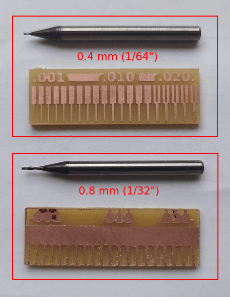
AVR ISP or ICSP
The above picture shows the idea about the ISP or ICSP ,which means in circuit serial programer. it use mainly 3 wires with respect to the GROUND or GND (GND is common) whic are...
- VCC - Postive Voltage
- GND - Ground
- RST - Reset Pin
- MISO- Master In Slave Out
- MOSI- Master Out Slave In
- SCK - Serial Clock
VCC,GND are the power pins for the programing provides from the programer and the reset pin is for resetting the microcontroller while the burning starts and also at the end,programing the chip is also called burning. MISO,MOSI and SCK are the data pins used for burning microcontrollers.SCK is clock for sending the datas through MOSI and SCK.
Circuit Schematics
we are not gonna design a new isp program,Instead taking from older design provided by the FAB Foundation.So this FabTinyISP is the one of the provided designs to mill out the pcb and also learn SMD soldering
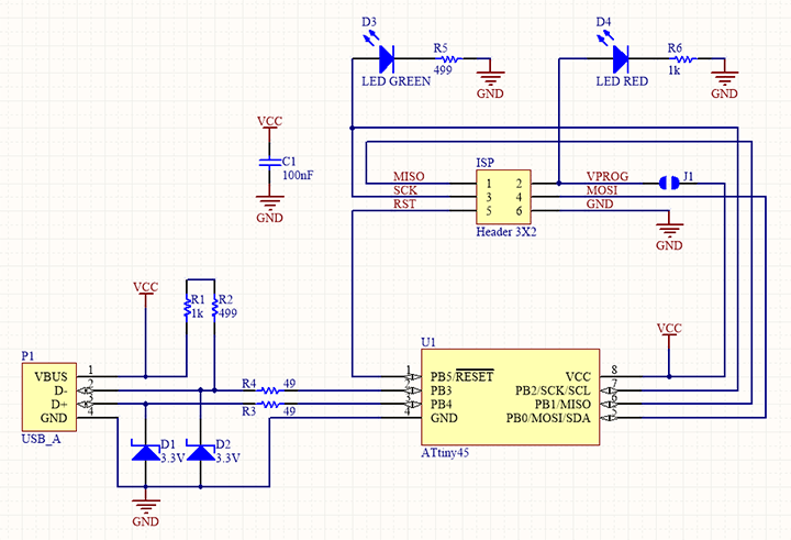
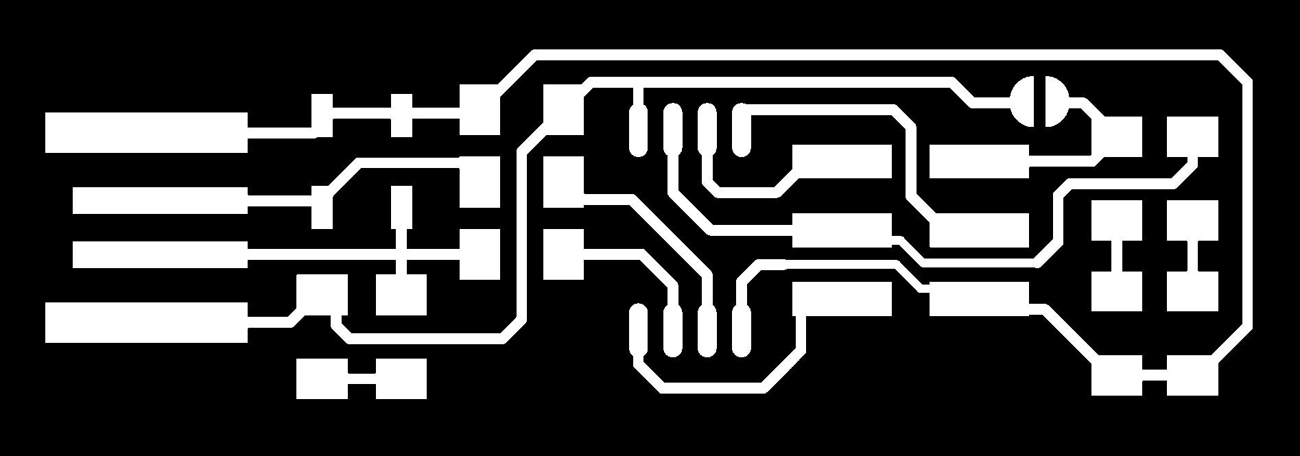
so this is the Schematic of AVR FAB ISP which is based on atitny45 so it also called fabtiny-isp.The chip is a 8 bit microcontroller by AVR so the for the fab isp the pcb design was made like a Pendrive like a plug and play USB device.see this altium file if need any modifications.so the sample pcb trace is given below
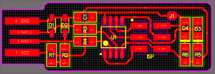
PCB Milling
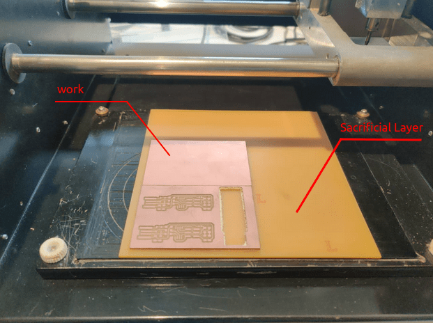
To start milling we should prepare the files for tracing the PCB.So I found FABtiny ISP files from FAB documentation.first we need to cut the traces then the outer line to cut the entire PCB for that fab provides FR-1 graded PCBs which is made for milling very friendly for us to work with it.We use a sacrificial layer on the bed to not damage the bit and as well as the bed of the machine.then I placed a pice of the coper clad plain board to cut out the FABtiny ISP
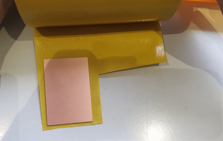
I used the double sided tape to stick the FR-1 board on the bed above the sacrificial layer
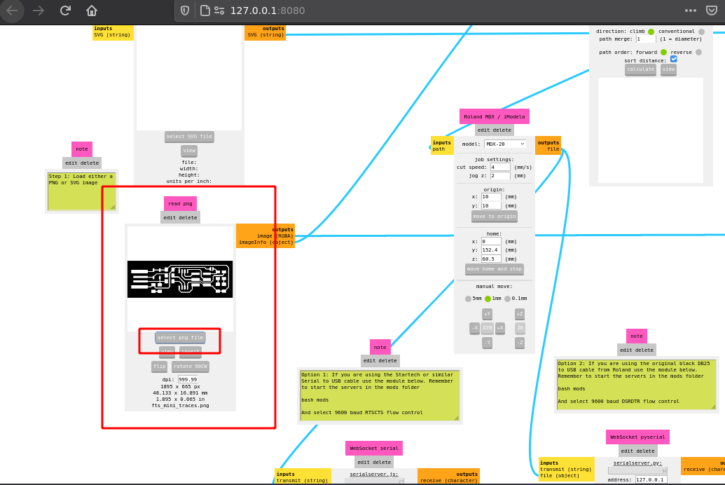
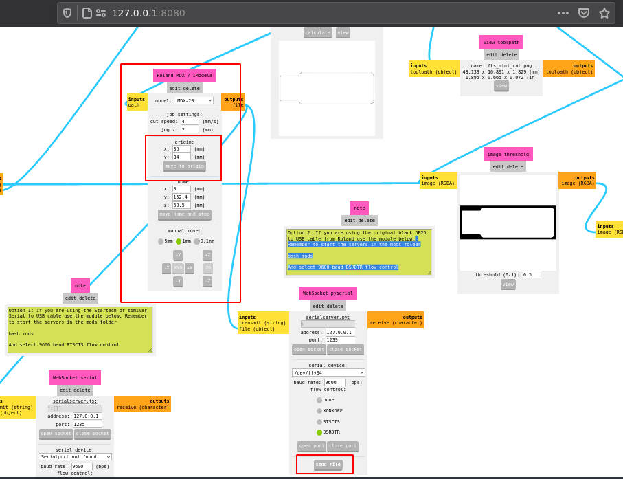
after the placement of the FR-1 Coperclad Board turned on the machine seted the view (home) to X0 Y0 Z0, then I placed the 0.4 mm (1/64") milling bit in the spindle chuck and sets the z home manually using the z up and down buttons on the machine .The bit touched the pcb top surface,now the z is set ,then I started FAB Mods webapp and opened the FAB MODS PCB mill program for MDX 20
Then loaded the PCB Trace cut png file provided in the FABtiny ISP documentation
The png file dpi size is 1000,if I put other values the dimensions gonna change.you can download the file from here
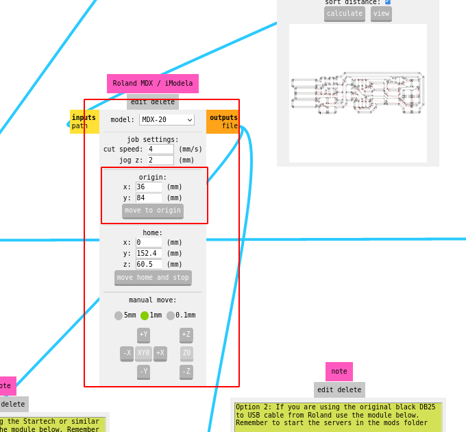
After loading I set the new origin at starting of my work. By editing the value in the FAB MODS,X-36 &Y-84
After the homing I inserts the o.4 (1/64") mill bit and tightened both spindle screws with an Allen key set carefully
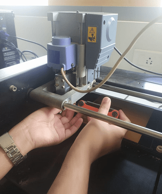
then manually sets the z probing like the end mill bit just touching the work surface with helps of z-up,z-down button on the machine
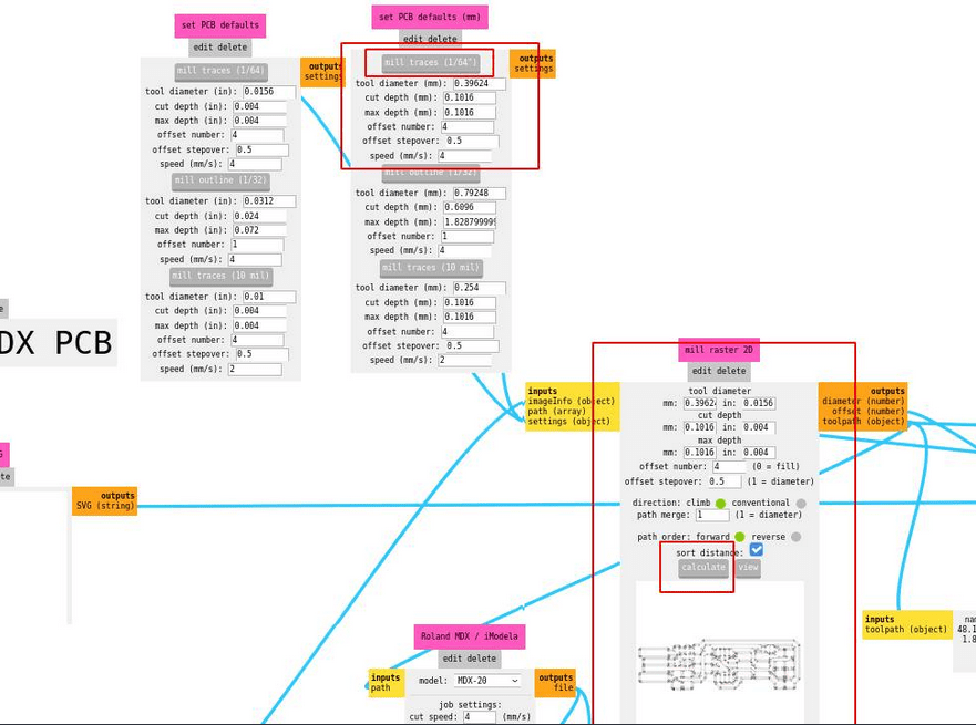
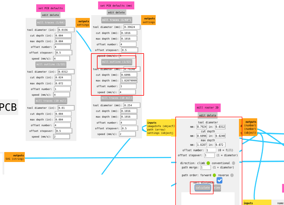
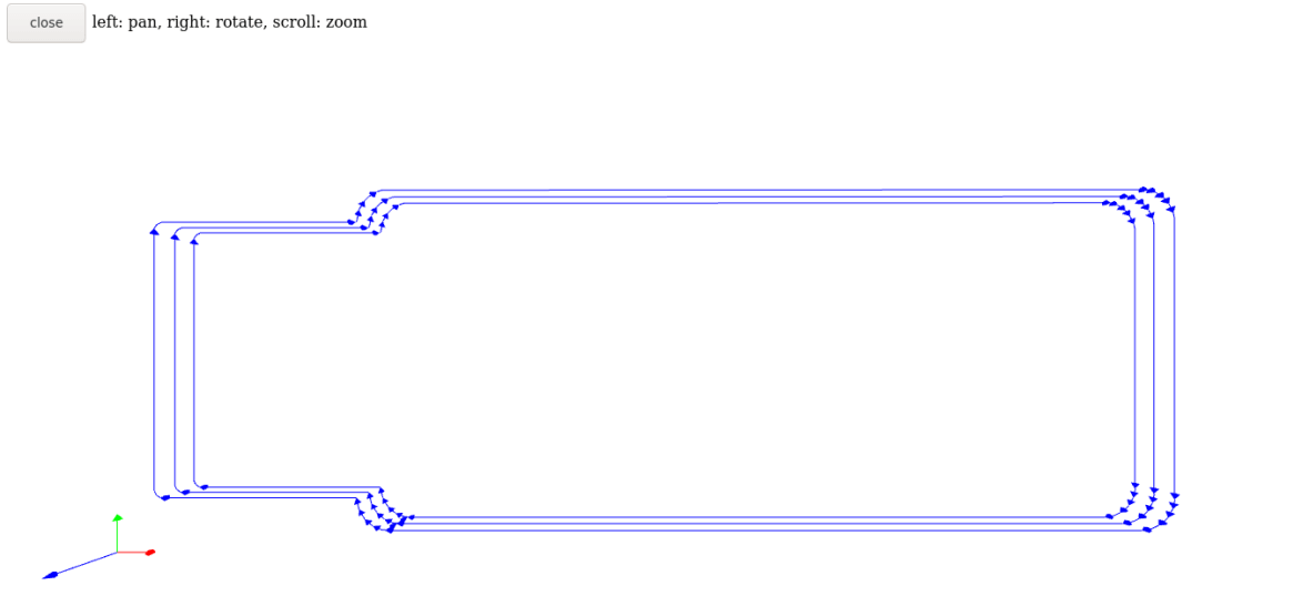
Back to mods,selected the 0.4 mm (1/64") mill bit and clicked the calculate button that opens a simulated path of the pcb traces
we can also see the fab mods other modules which shows the offset , cutting pats etc...
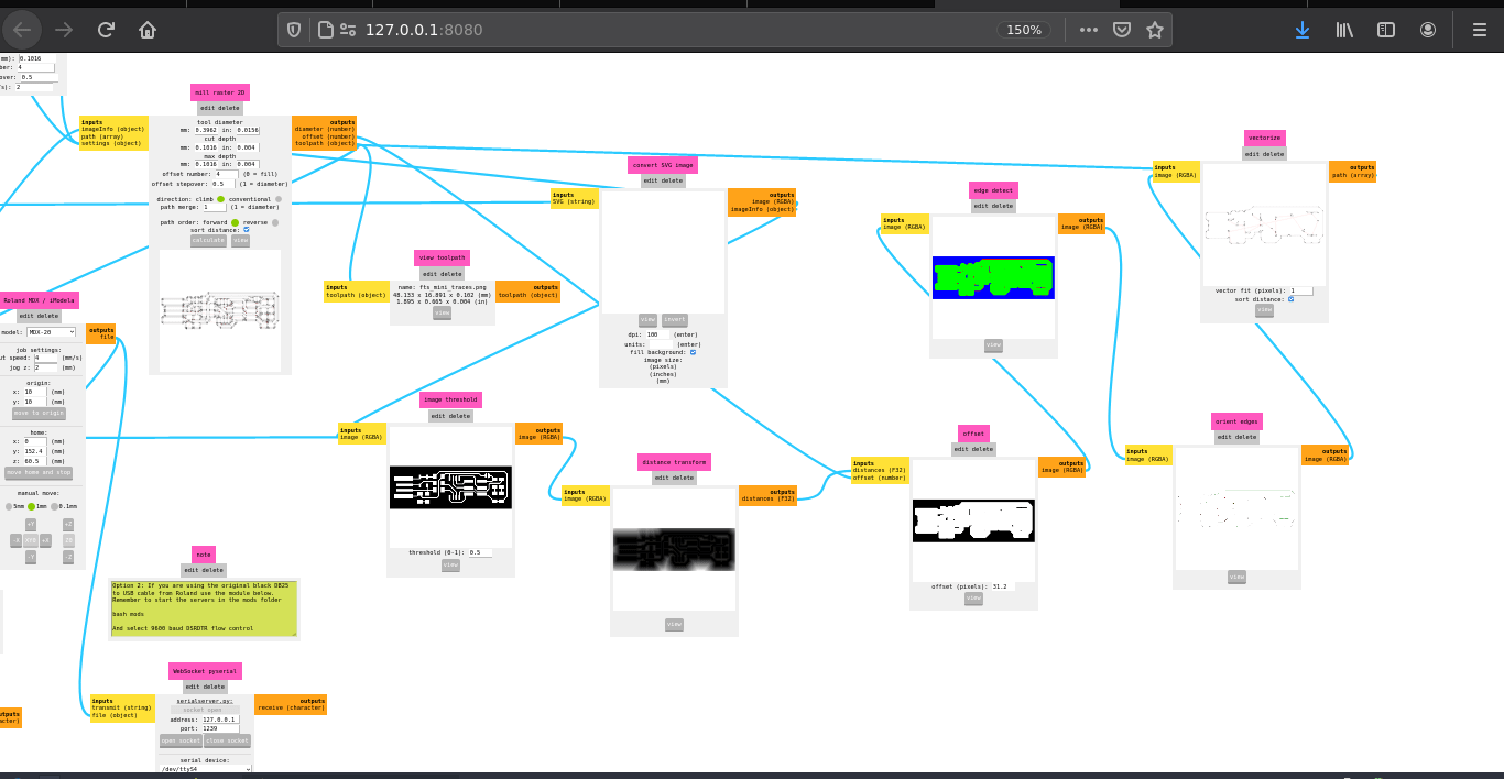
then I click send the file from mods to MDX 20 milling machine
the machine starts to mill the pcb traces I took a time laps video of it
after the traces milling process I loaded the given cut out traces in mods and changes the 0.4 mm (1/64") mill bit to 0.8 mm (1/32") cutting bit and rests the z height again for the new bit

You can download the cut traces from here ,remember the dpi value is always 1000
I selected the 0.8 mm (1/32") cutting bits in modes,so the cutting depth sets for 1.878 mm,it depends the coper clad board
see the mods simulated path passes for the cutting
then I moved the milling head to the same origin that used in cutting traces ,if its a different origin not gonna cut out already milled pcb so it is mandatory to make sure the origins are same for both cutting and tracing
After setting the origin I click send button in the fab mods,then the machine started to cut out the outer path of the pcb see the time laps
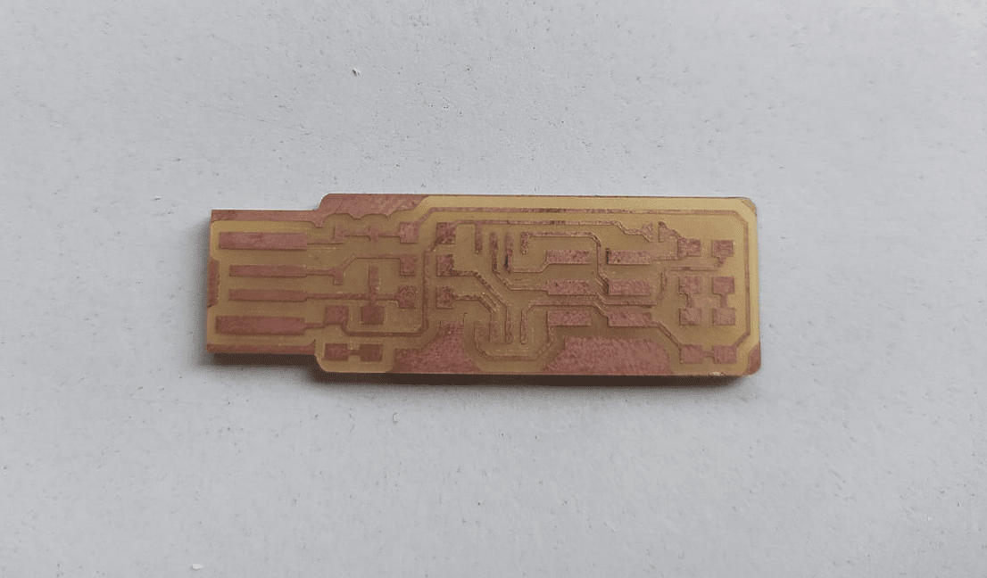
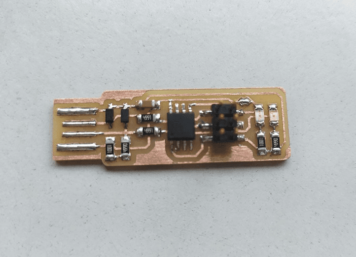
So,that's it successfully manufactured a Milled PCB !!
Collecting Components
Next process is to solder the Components on the PCB like finished PCB, for that I collected some SMD components which are suggested for the circuit from ,the FAB LAB Kochi's Inventory store,The components suggested by the fab tutorials is given below
- 1x ATtiny45
- 2x 1kΩ resistors
- 2x 499Ω resistors
- 2x 49Ω resistors
- 2x 3.3v Zener diodes
- 1x red LED
- 1x green LED
- 1x 100nF capacitor
- 1x 2x3 Male pin header
- 2x 2x3 6 Pin Female IDC Socket
- 1X 20 CM 6 pair Ribbon cable
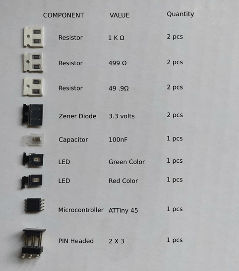
The above picture shows the components that I collected from the lab's store.the fab instructors suggested to make list on a white paper before taking components from the store.But I did not follow because,I'm coming from a electronics engineering background well experienced with 1000 different electronics components so I decided to not use a white paper list
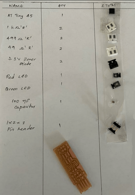
The above picture is an example of white paper listing. The picture borrowed from a friend Alfia M.If you are a beginner not recommended to do my way follow like her way
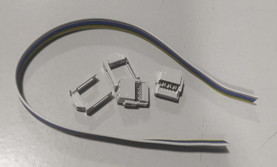
This cable needed for ISP programer to connect other the target board or Micrcontroller through the 3 pin along with the VCC,GND and Reset
Soldering
Soldering is a welding process creating a joint between two conductive leads or metal surface by hearting and tinning ,mostly iron and coper.so need a better practice to make good soldering joint.I started to make circuits when I was 12 so I got the experience of 10 years of soldering circuits which includes wires,PCBs,THT and SMD Components etc..
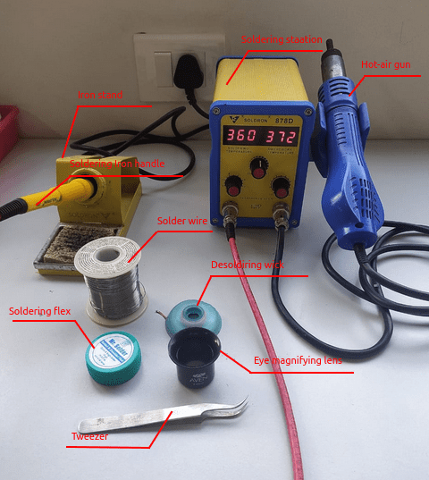
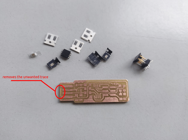
Those are the main Tools I used for soldering FABtiny isp PCB.The soldering iron tip is pointy,perfect for soldering SMD components.then I prepared the components and the milled PCB for soldering.used a sand paper to rub the surface of the PCB also removed the unwanted trace from the pcb like suggested in the fab tutorials.
sets the soldering station temperature 320-350 range.for easy soldering and aligning the component properly I sticked the pcb on block
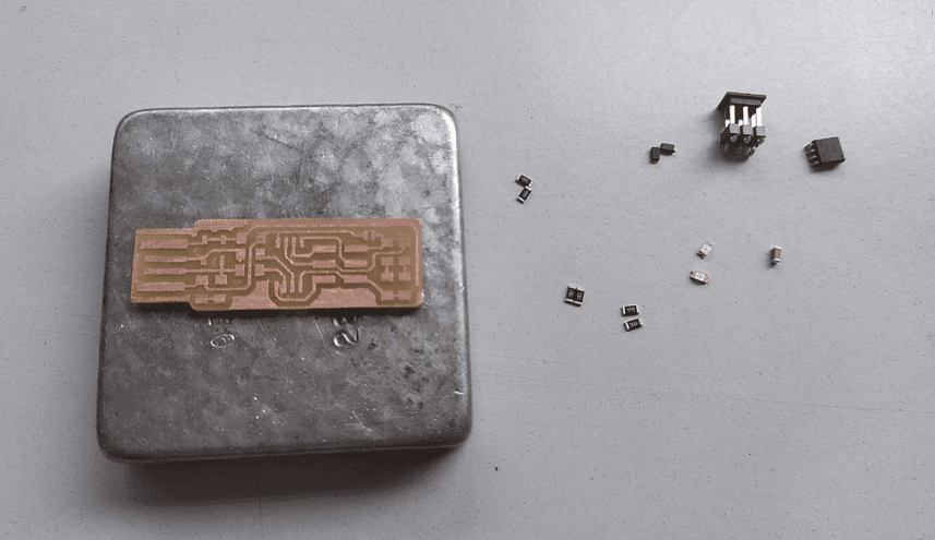
in order to solder SMD components first we have to put some solder tin on one pad of the component then care fully place the component with the tweezer and hold it in left hand then take soldering iron and heat together while aligning the component then solder other leads of the component. repeat those steps for every component But,I have experience on soldering SMD components and I did 100 PCB's so I know a fastest way to solder all the components together see the time laps actually I done it in less than 5-6 minutes.
So that was fast. The Soldering all done! beautifully. Better Soldering practice give good results.
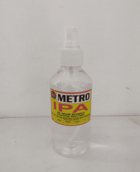
Then I cleaned the PCB with IPA (iso Propyl Alcohol).That's helps to remove unwanted flux and soldering dust partials from the board.
Checking and Visual Inspection
After the soldering officially its ready to program.Before that we might wanna inspect anything wrong or not.I'm confident about my ISP and also made sure nothing wrong visually
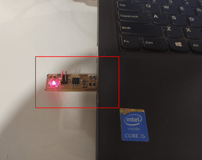
Then I plugged into my laptop's USB socket It's lighted up!. The Power LED is on (red color) so the board connections are OK in Power level
Making the ISP cable
Creating ISP cable isn't that hard.The IDC sockets and the Ribbon cable make the process very simple all we wanted a rubber hammer to crimp the connectors with the cable
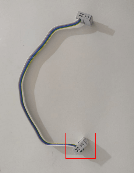
I crimped the cable wit the help of the instructors.there is slight chance to brake the IDC connector while crimping so must be careful with that
Programing the Attiny45
The chip on the ISP is an AVR Attiny series microcontroller from atmel. The source code and the program files for the Fabtiny ISP and step by step instructions are also provided in the Fab academy tutorials.
Setting up the Software and tool chain:-
To program the AVR microcontroller required to install the necessary softwares or tool chains for AVR programing such as AVR-GCC compailer.AVRDUDE flashing programs..etc..
The FAB tutorials strongly recommended Linux Operating system to work with so I set-up the tool-chains in my Linux pc
sudo apt-get install avrdude gcc-avr avr-libc makeTo install the tool-chains and libraries I used the above command in my terminal then it automatically downloaded from the internet and installed it my system
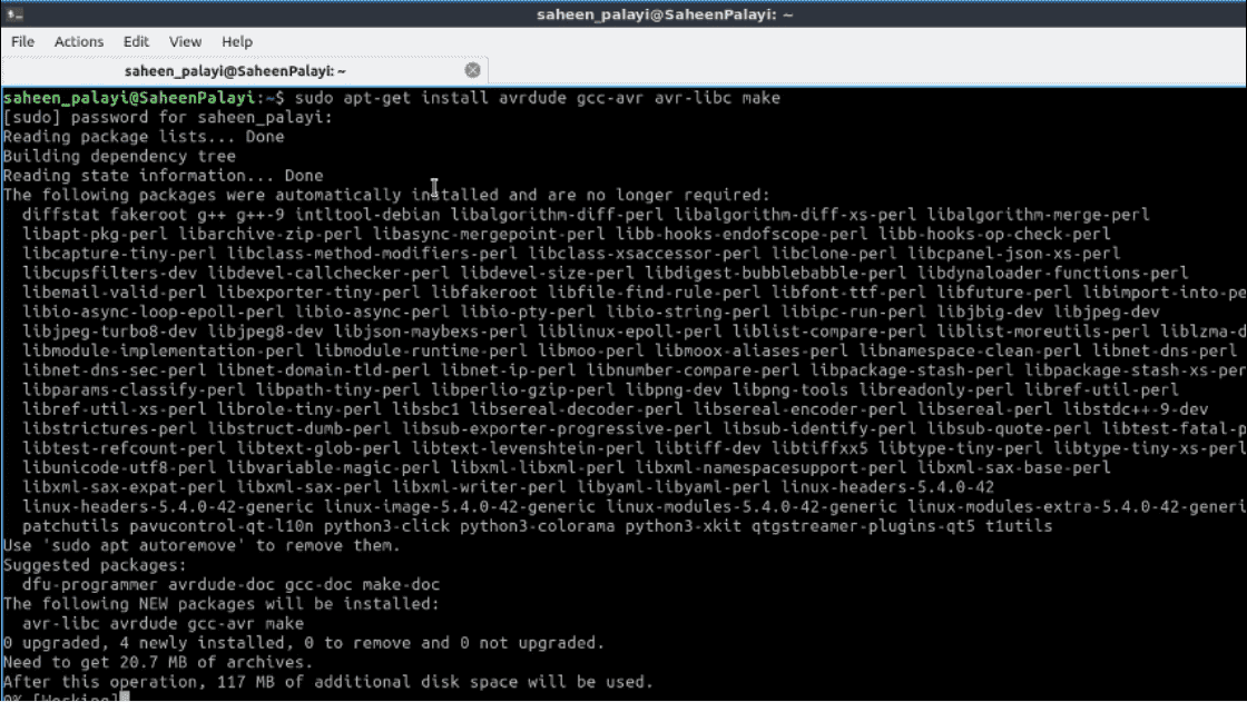
The tool-chains are ready now to program
Getting the Source file
The source file can be found from the Academanygithub repository.so I made a directory called 'avr' in my home folder then I downloaded the file to the folder
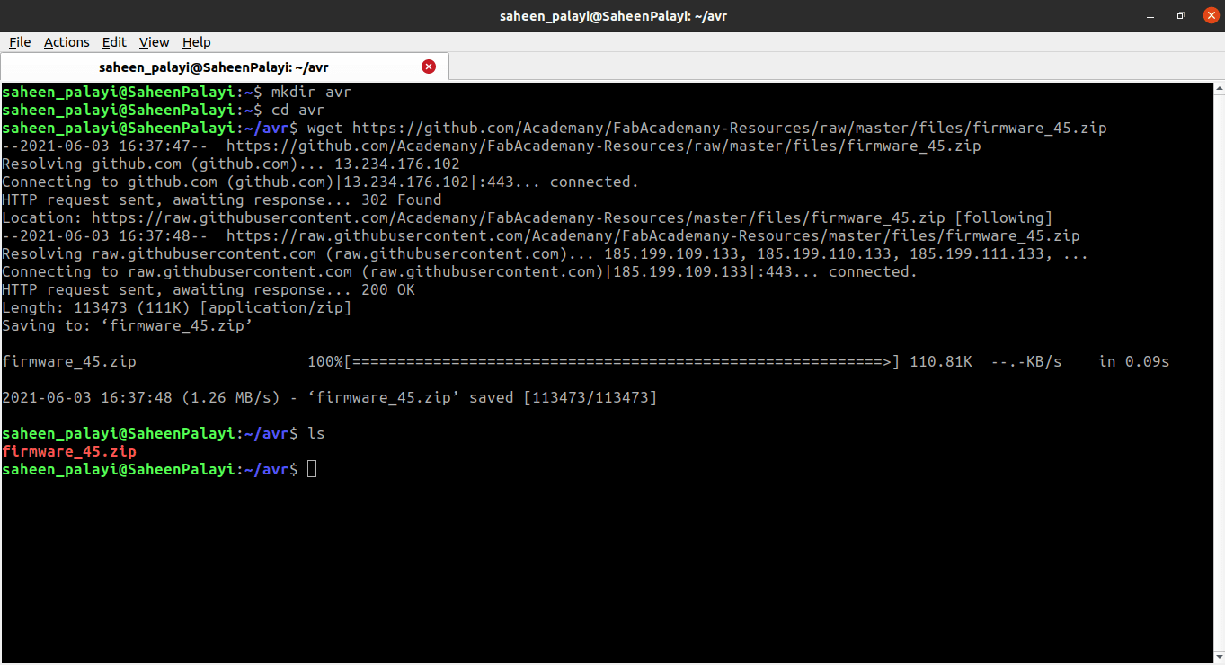
wget https://github.com/Academany/FabAcademany-Resources/raw/master/files/firmware_45.zipthen I extracted the file inside the directory
unzip firmware_45.zip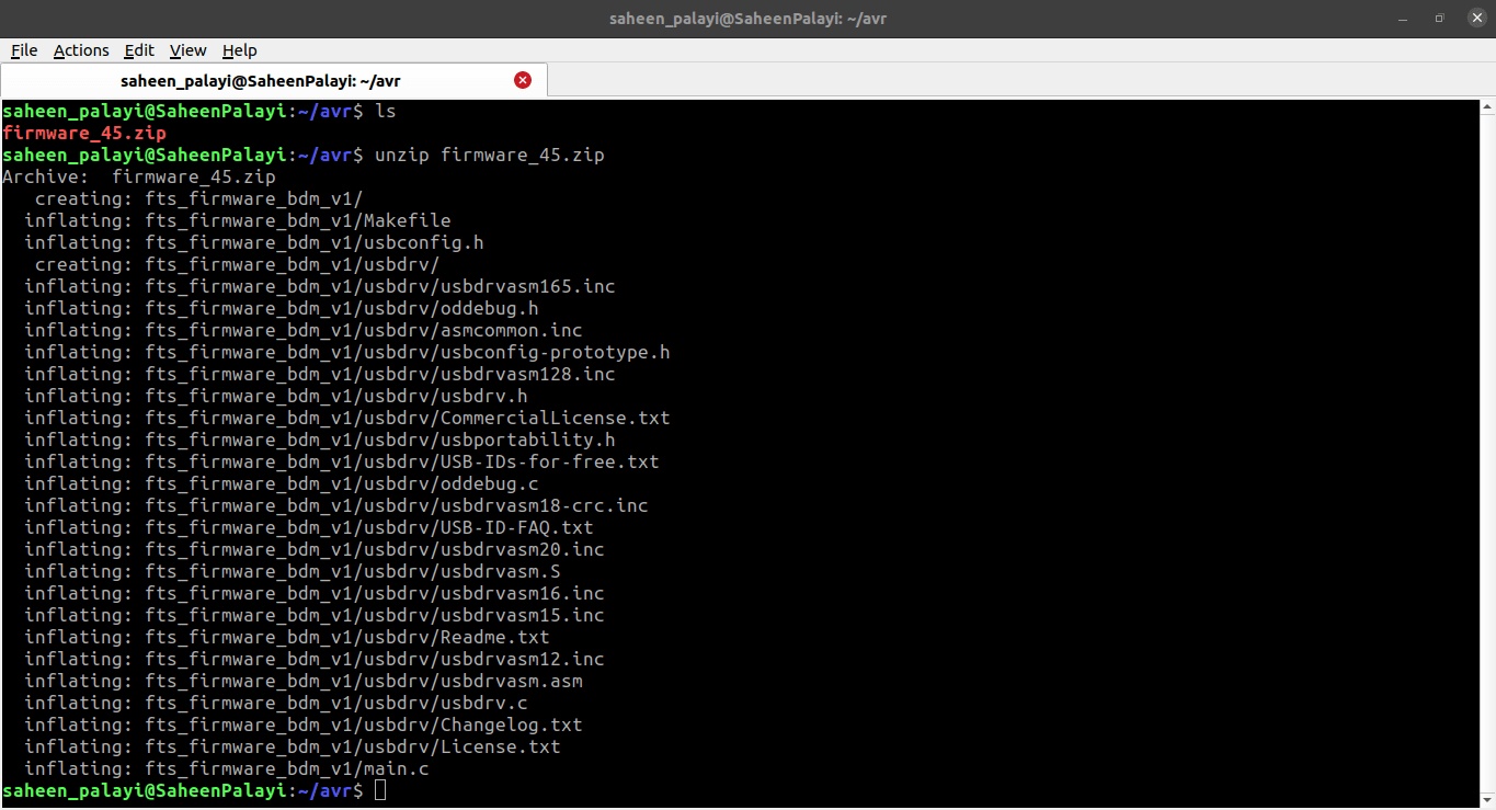
we can also do the download and un zipping manually
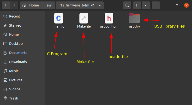
inside the unzipped folder we can see the source code in c and related libraries then the make files
creating hex and flashing...
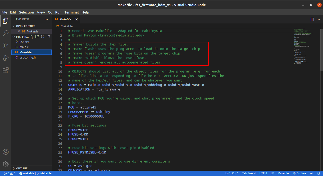
so the files and softwares are prepared for programing the Attiny45 Microcontroller all the instructions can be found in the make file
Another ISP programer required to program the Fabtiny ISP board that I made. So I plugged the ISP board to my PC through the 6-pin ISP cable wth the help of the ISP Programer of the FABLAB kochi
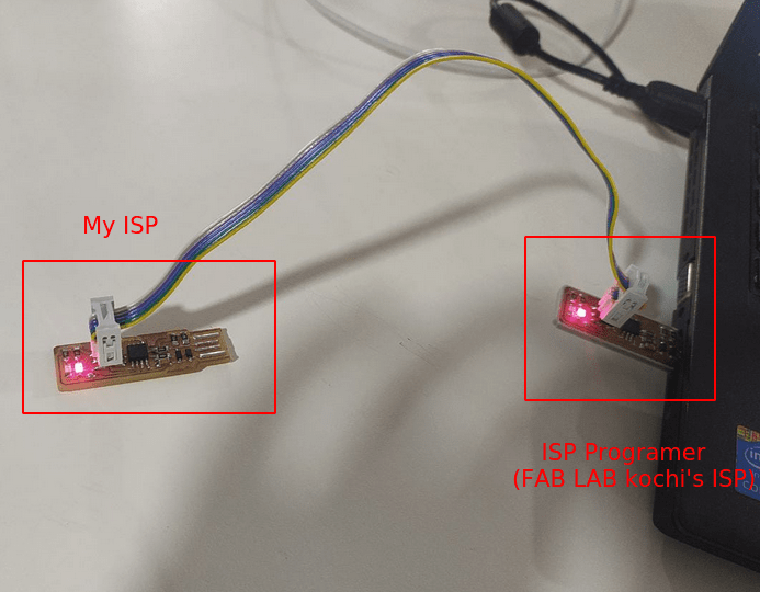
If we connect the cable correctly the red LED will power up. Now the hardware setup is ready for programing
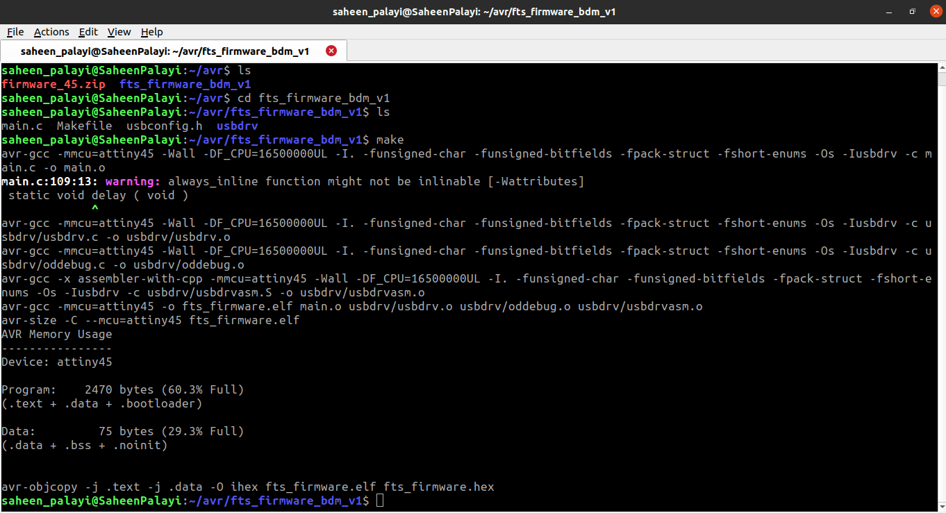
Then I changed the directory inside unziped folder and entered the below command as instructed to compile the code
make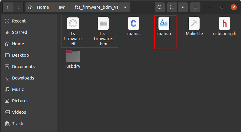
If we check the directory after we can see that new files are created with '.O' '.elf' and '.hex' extensions. The '.hex' file is used for flash to the chip
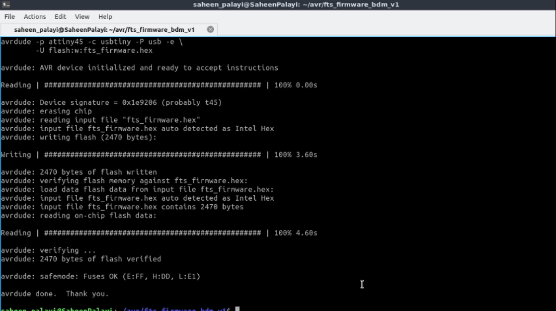
make flashThen I entered the 'make flash' command to flash the hex code to the atitny45 chip on my ISP
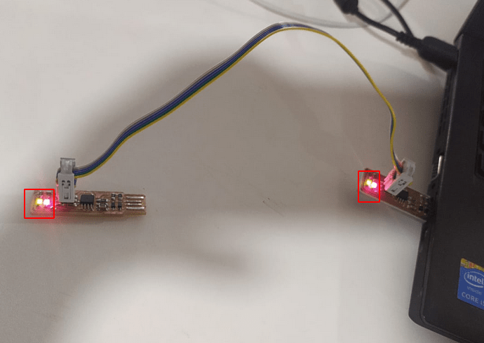
while flashing the green LED will light up to indicate the data communication happening .
Now the flashing is done next step to flash the fuses using the below command
make fuses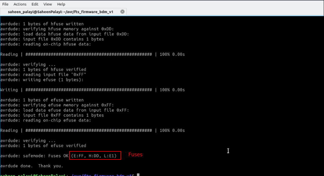
Yah! the fuses are done!. Now I have to check my ISP working or not. So I plugged my ISP to the USB port of my PC then entered the command below
lsusb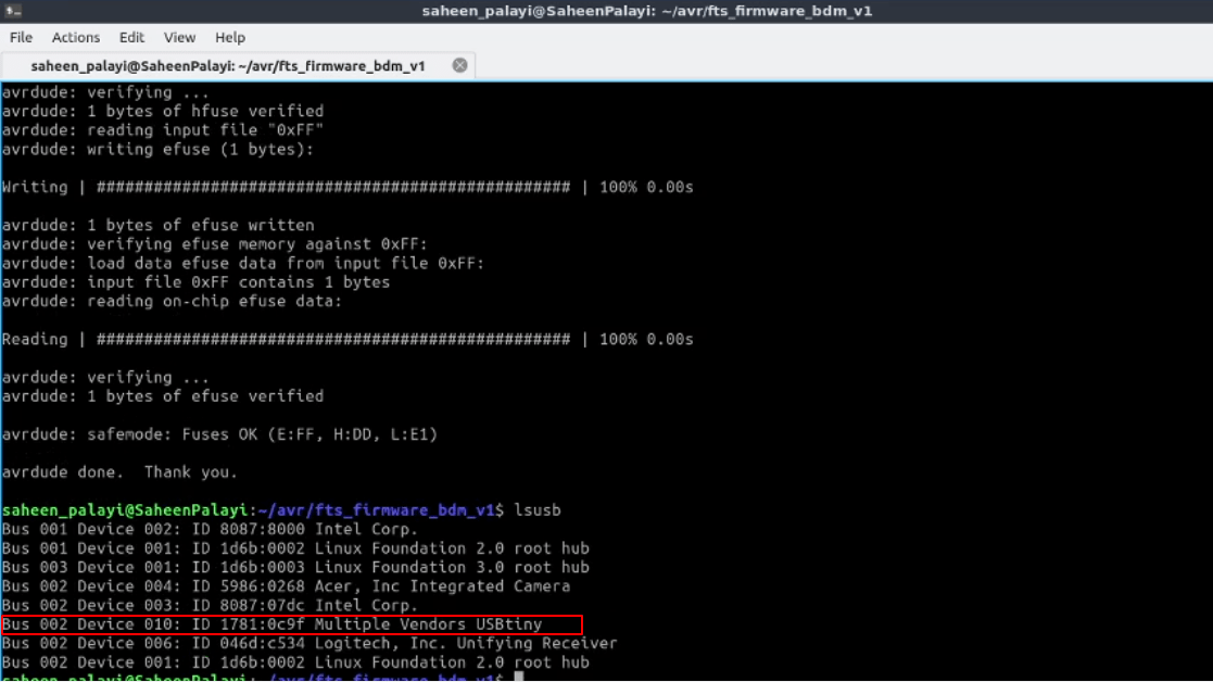
The result of the command shows us the list of the USB devices plugged in to the PC in between them we can the 'Multiple vendor USBtiny' device that is the FABtiny ISP
didnt detected first time I tried because there was something wrong with my FABtiny ISP.I troubleshoots and finds out two resistors aren't in correct values
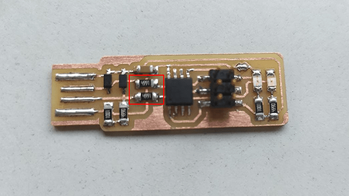
The resister I soldered was the '4991' labeled or 4.99 K valued resister.But I took from the correct container at the Inventory room.My be somebody missorted the components accidentally before.Any way I found the correct one which is '49.9 ohm' and labeled as '49R9'. It's better to double check the resistors before soldering. All resister labeled on the top in 3 Digit or 4 digit I used this online Chip resistor calculator to check the values.
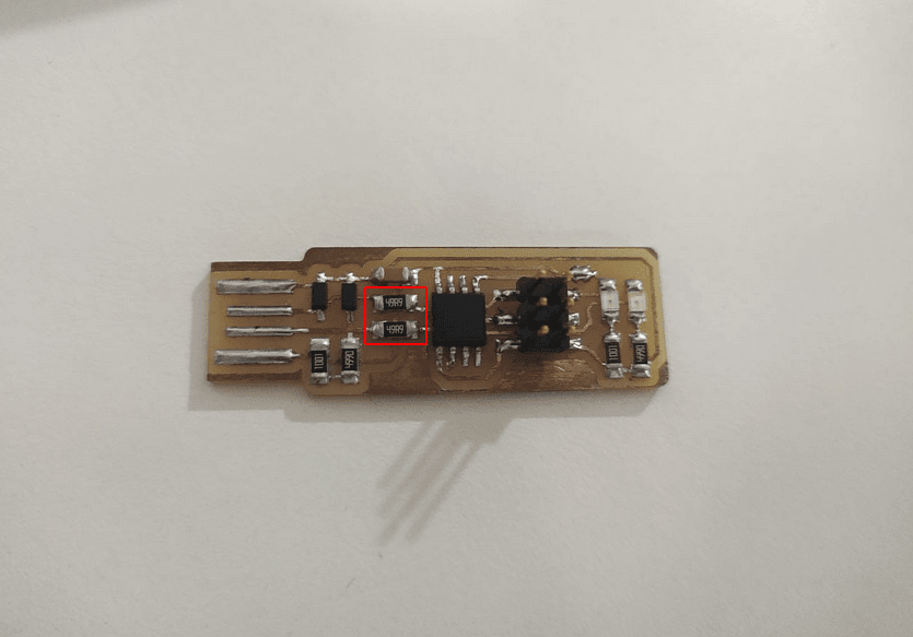
So the resister are replaced with correct value resistors. SMD De-soldering is an interesting job than soldering
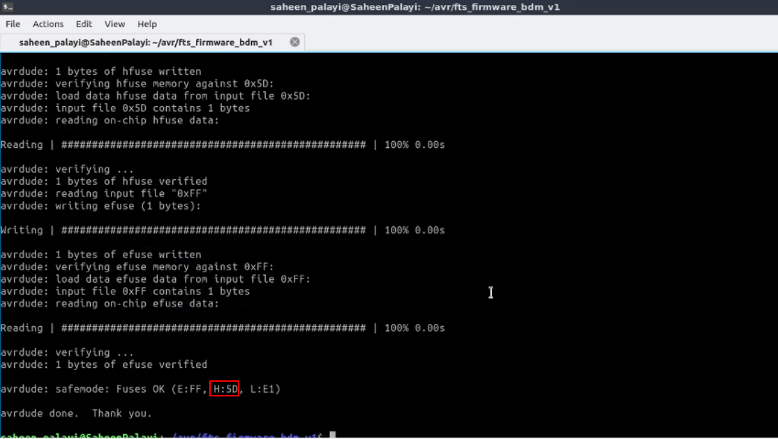
make rstdisblThen I disabled the Reset fuses of the Attiny45 using the command in terminal and it rewrites the H fuses to disable the reset function.
At the time micrcontroller program with ISP protocol the reset activates for milliseconds to reset the target micrcontroller.here we are disabling the reset function to not reset it's self while programing
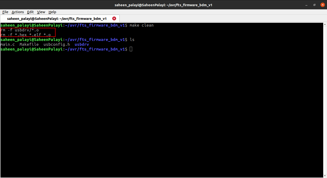
make cleanthen I use the 'make clean' command for removing the all auto generated files which created while compiling
So finally my FABtiny ISP is ready to rock, It will be use full for upcoming assignment.It was totally new way of production method for me
Fiber Laser PCB Production
In our super fablab we have a Fiber/CO2 laser engraving machine have capable enough to engrave metal surface. This advantage can be used to engrave PCB's for removing unwanted copper parts. Neil was mentioned while the PCB production class and It's also done before in our LAB.
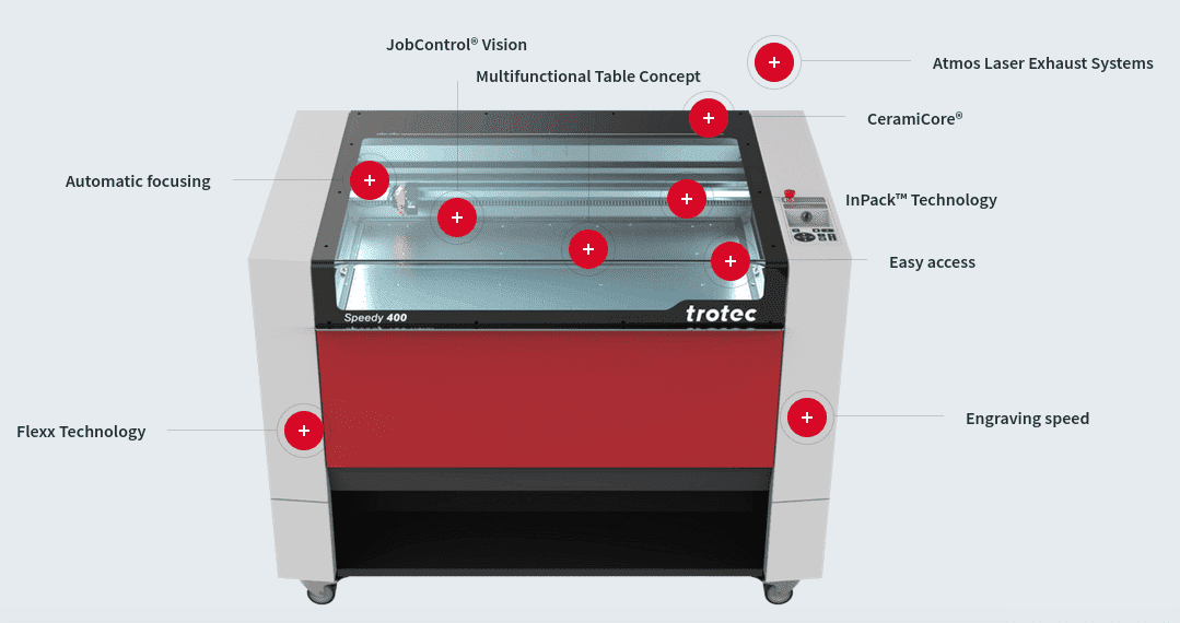
The Trotec speedy-400 is an advance version of speedy-100 this makes many things easy. It has larger cutting area and auto focussing features.
Actually this method isn't necessary for this week assignments so I did this later in a free time for a learning purpose. So I've decided to make a USB Mini/Micro Breakout board and a line test to know the design rules.The Breakout board PCB is designed by my self to check that I can solder a micro USB connector in a PCB which I made in Fab Lab or not. Mr. Joel George Alex Helps me to do the Fiber laser engraving
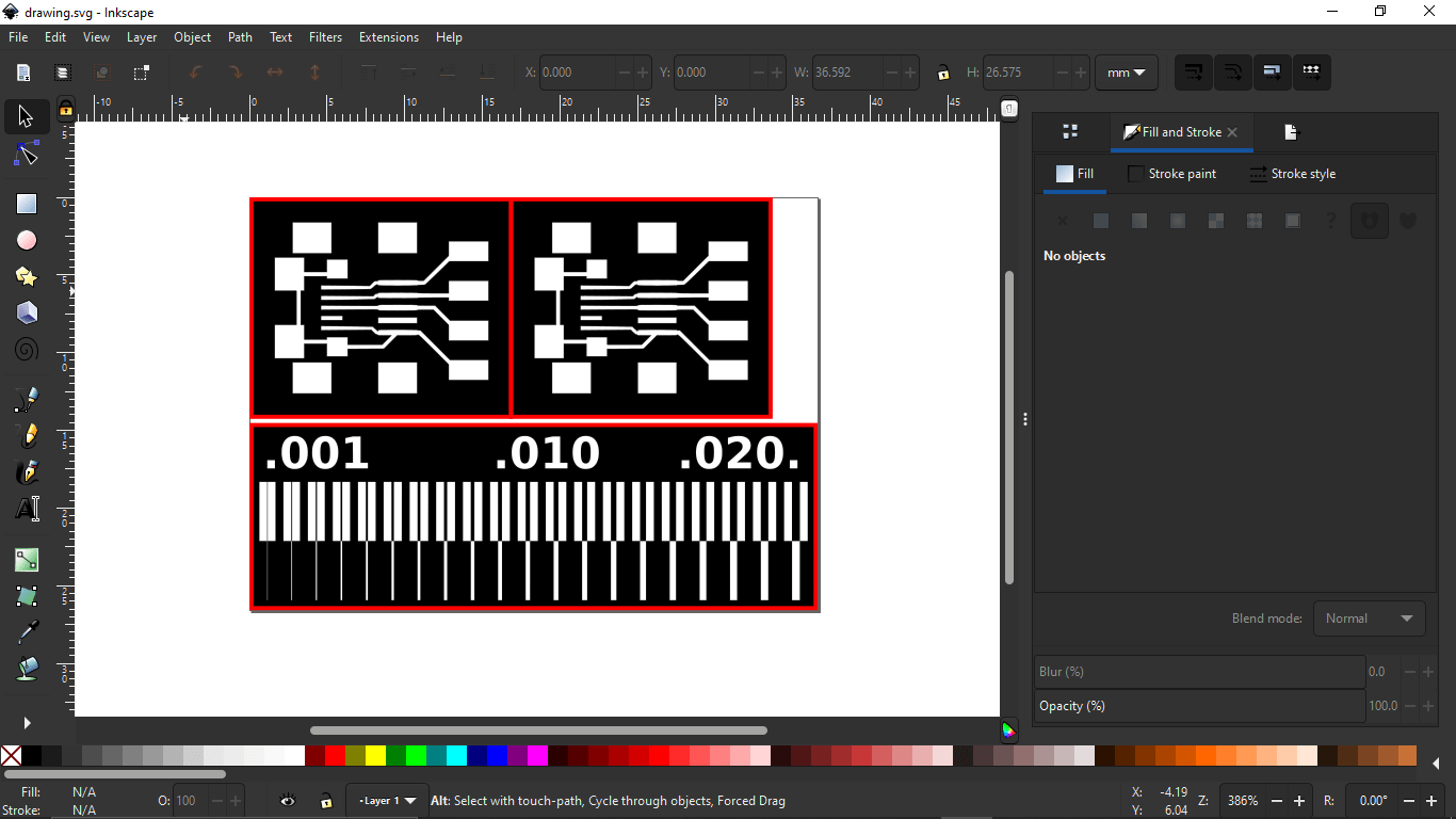
In order to engrave we opened the trace Files and taken bitmap trace from the png file then nested them for laser engraving.The rules are same as before black for engrave with no stroke and the red for cutting with no fill.
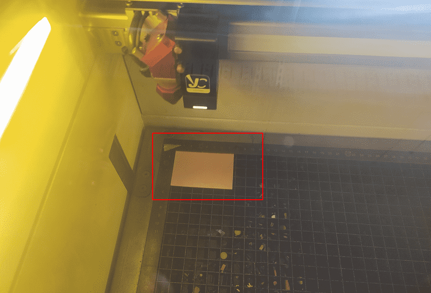
We placed the Coper clad PCB in the corner of the Laser cutter's Bed. Next we need to set the focus.one of the good thing is this laser engraver has Auto focussing feature ad that's very cool!.
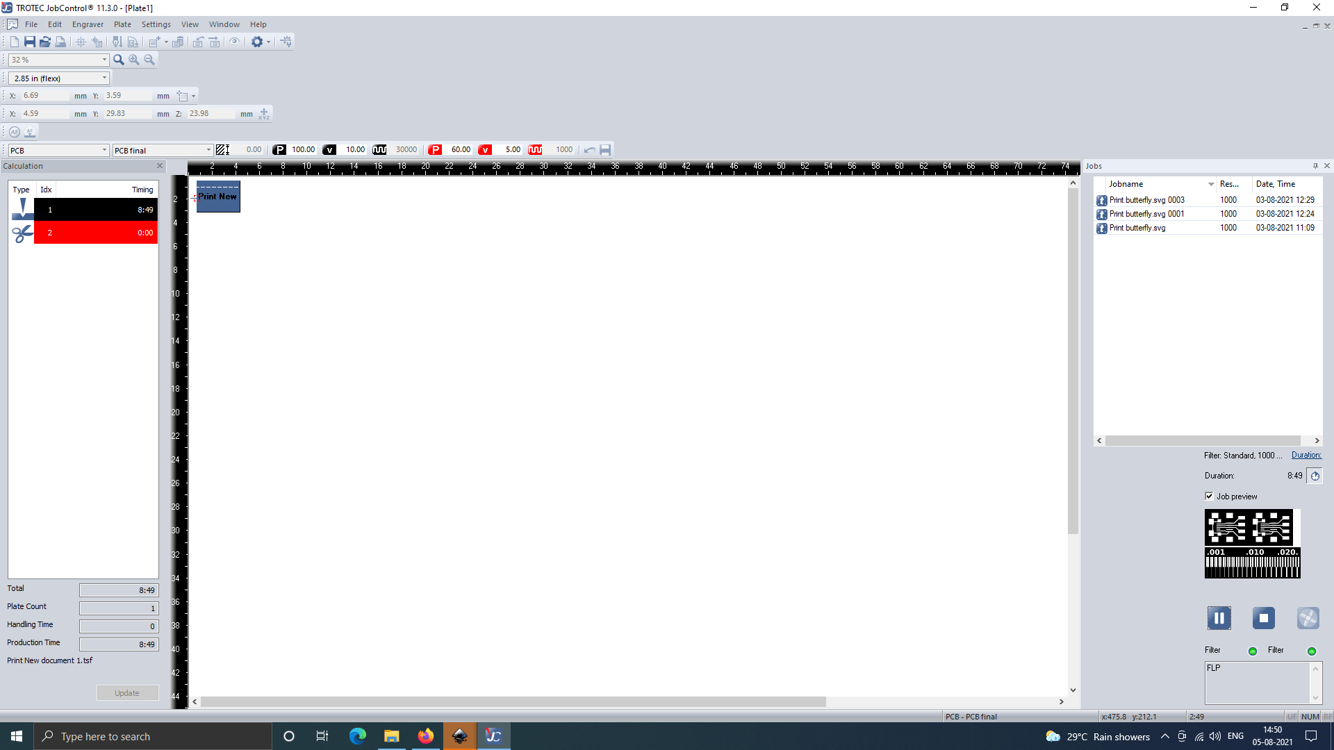
After placing the coper clad we opened the Trotec software in the PC and placed the job in the corner.
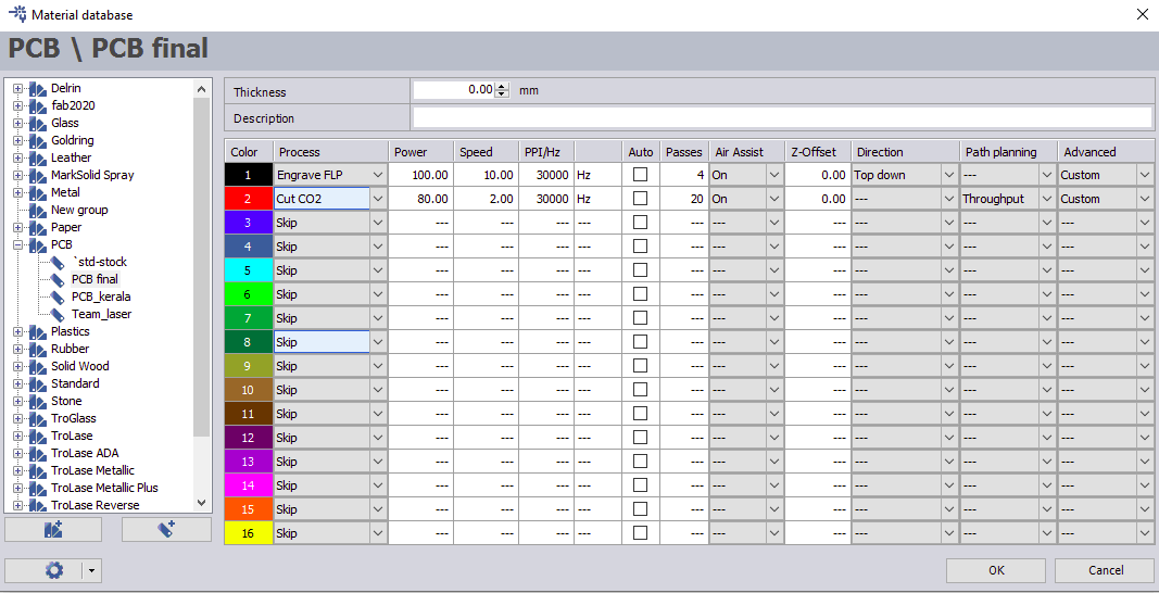
This is the setting we used for engraving the PCB first we skipped the CO2 cutting and set for only engraving..
See the Complete engraving process in the above youtube video. we ran 4 pass twice to Ignore any chance for getting copper strings between pads. The cuttling wasn't come out as expected.
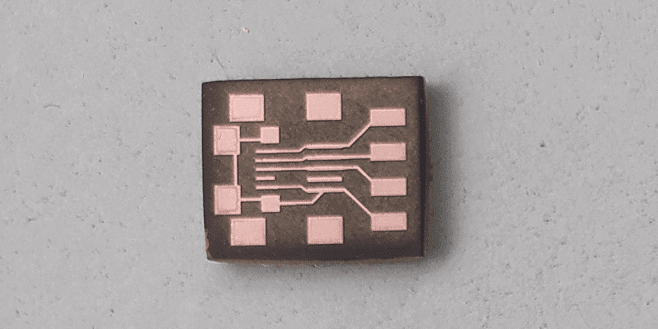
This is what the results looks like, the cutting was unsuccessful and that killed the beauty of the entire board.It's not a good idea to cut the FR1 sheet in laser cutter.so I cut them using a dremel tool by hand and then cleaned with IPA (Iso Propyl Alcohol).
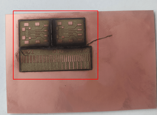
Line Test:-
The line test results shows how much we can engrave. It's look like, it's possible to achieve 1 mill traces and space between in traces with laser engraving process. but The 1 mill trace came off the board while from my observation it's better to keep 5 or 6 mill while design for PCB laser engraving process.
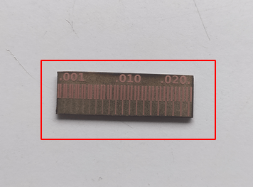
Here is the USB Micro/Mini Breakout board laser engraved along with the line Testing.It's looks like we can achieve promising results like this.
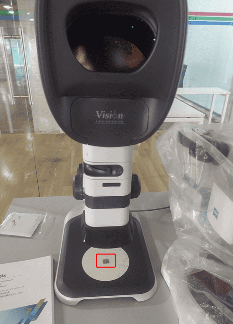
For the quality Inspection I placed under the Vision 3d microscope in our super fablab I's awesome and very satisfying to see through he 3D Microscope.
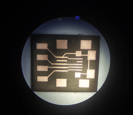
Here is the picture what I saw in the microscope It's feel like 3D and the results are very pretty. And also no strings and any unwanted traces all engraved very well
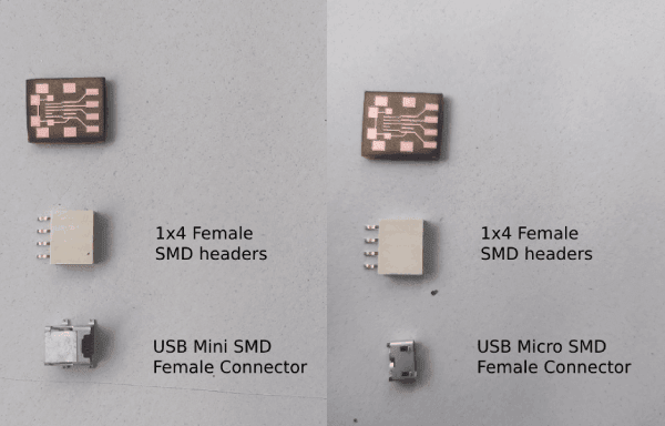
I've Collected all these components to make and test the breakout board. The connector soldering is a tricky one needs to follow special soldering method to solder them without any pin shortages.
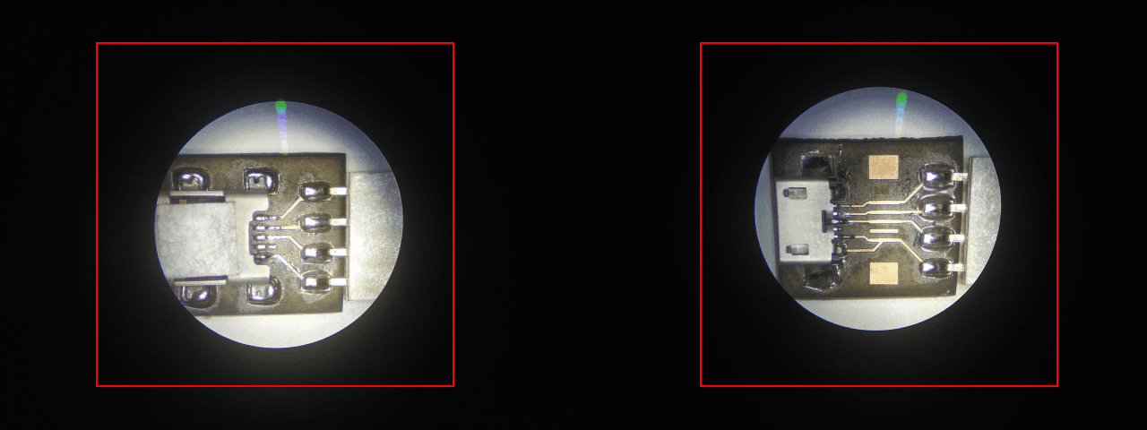
The figure shows the Microscopic view after I soldered the both mini and micro connectors in each board.It's cool!
Resources
References
- Fab Academy Electronics Production classes
- Roland MDX 20
- AVR FREKS community website
- FabTinyISP
- Trotec Speedy Laser Engraving Machine
Downloads
- Resolution test
- FabTinyISP PCB Files
- FABTinyISP firmware_45.zip
- PCB Laser Engraving Files