Week 6
Assignment 1-Redraw an eco hello world board.
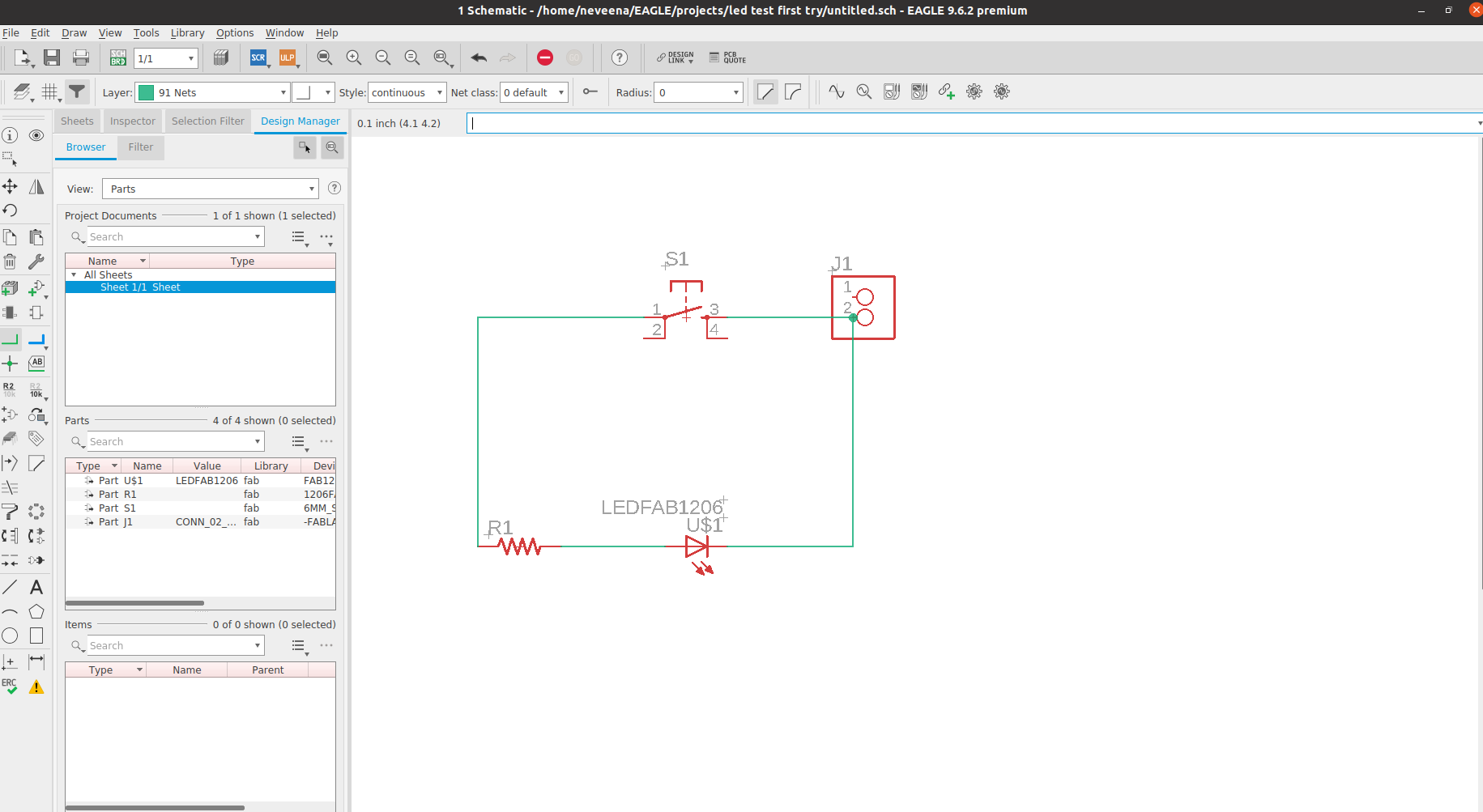
We were recommended to use EAGLE software.EAGLE is a scriptable electronic design automation application with schematic capture, printed circuit board layout, auto-router and computer-aided manufacturing features. EAGLE stands for Easily Applicable Graphical Layout Editor and is developed by CadSoft Computer GmbH.
Intially we were introduced to some components and other basics of electronics by our mentor. i found it a bit challenging to understand it first because i have never been into electronics and this was my first time. Step by step i found it interesting.As I do not have any experience with PCB design softwares, I decided to followed what my instructor suggested. He briefed us on how to install libraries, add parts, connect wires and edit schematic layout in Eagle and asked us to tryout any simple design before going into this week’s assignment.

It was my first experience with eagle , we learned how to design simple cicuits to get an idea.
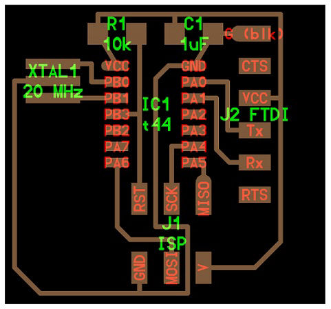
COMPONENTS
1.ATtiny44 x 1 - This is a programmable micro controller chip that controls all the parts on the board and is programmed from the computer.
Let us say this is the brain of our Board.
2.XTAL 20HZ x 1 - This Resonance crystal acts as an external clock for the circuit.
It needs the input traces to be connected to two pins on the board and the ground trace to the GND circuit.
3.Resistor 10K x 2
4.Resistor 499ohm x 1
5.Capacitor 10uf x 1 - this is a device used to store electric charge, consisting of one or more pairs of conductors separated by an insulator.
This will help filter devices to remove voltage or signal spikes in our circuit.
6.Push button x 1
7.ISP header x 1 - the 2x3 pin header that connects the FabISP to our newly created chip(ISP - In System Programmer.
8.FTDI header x1 -the 1x6 pin header that connects to the special FTDI USB cable (FTDI is Future Technology Devices International -
The company that makes a special usb cable - and drivers that let us write to the 6 pin output like a standard serial port.)This will connect
the circuit to the computer to both read the program and power the board. It’s VCC and GND pins need to be connected to the respective VCC and GND circuits on the board,
and it’s Tx and Rx pins connect to the two free pins on the microcontroller.
we were asked to hand draw the schematic of the board before using eagle to draw the schematic.
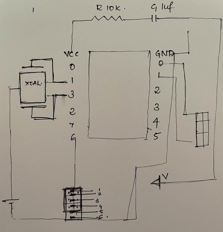
The above shown picture was just a try, it really does have mistakes. I tried learning the schematic representations of some components. and after drawing the schematic we got an idea how to do it in the software for a beginer like me it was one major step.
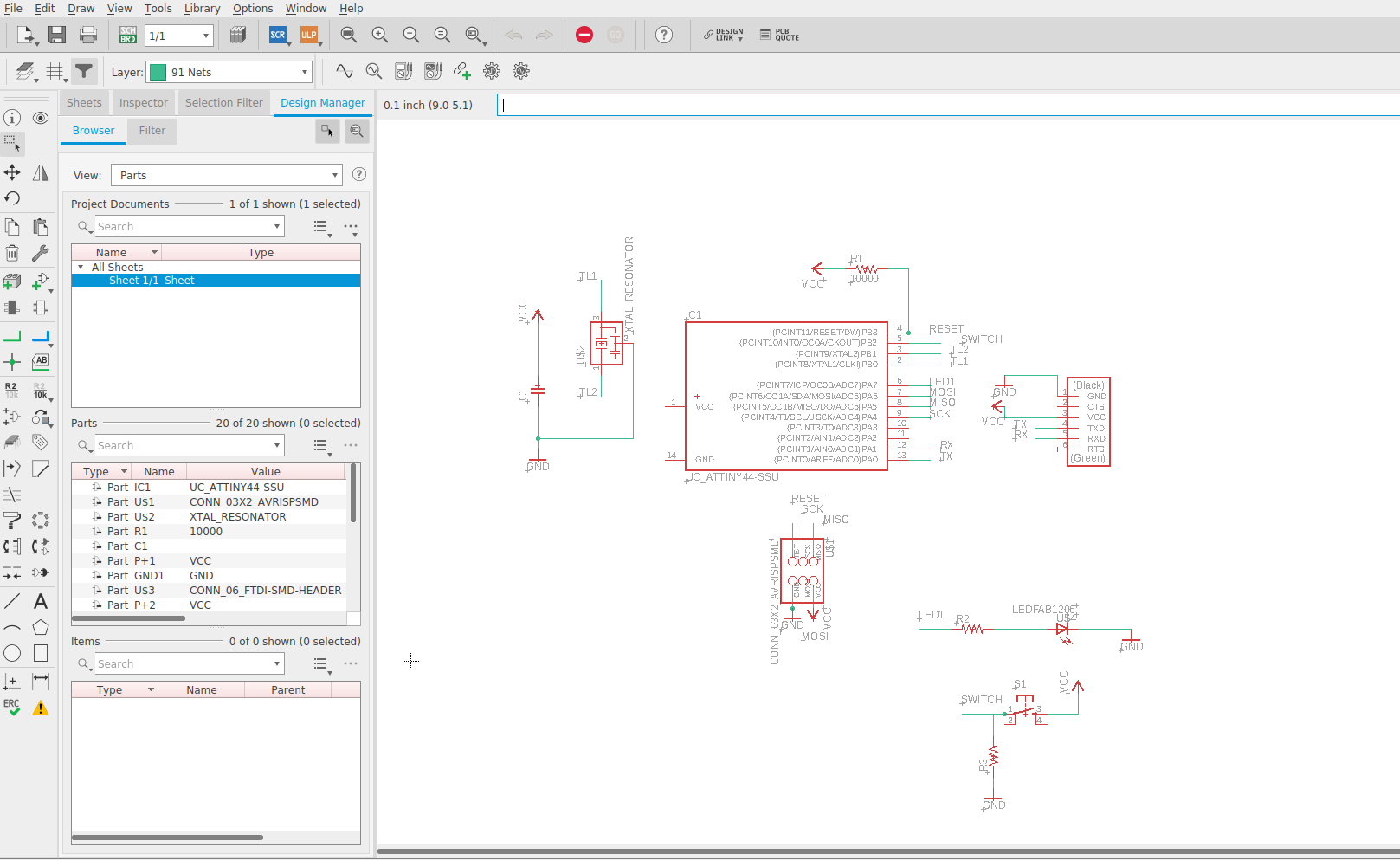
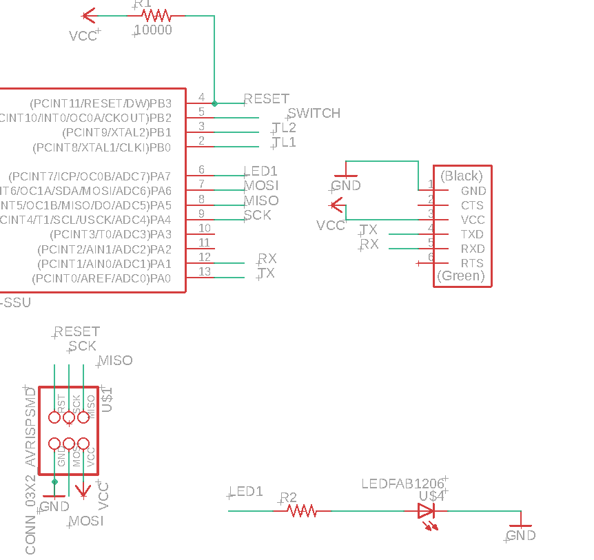
I have connected the net by giving similar names to the ends, which helps in reducing the confusion as well as it
maintains the schematic in a neat way. The picture is shown above.
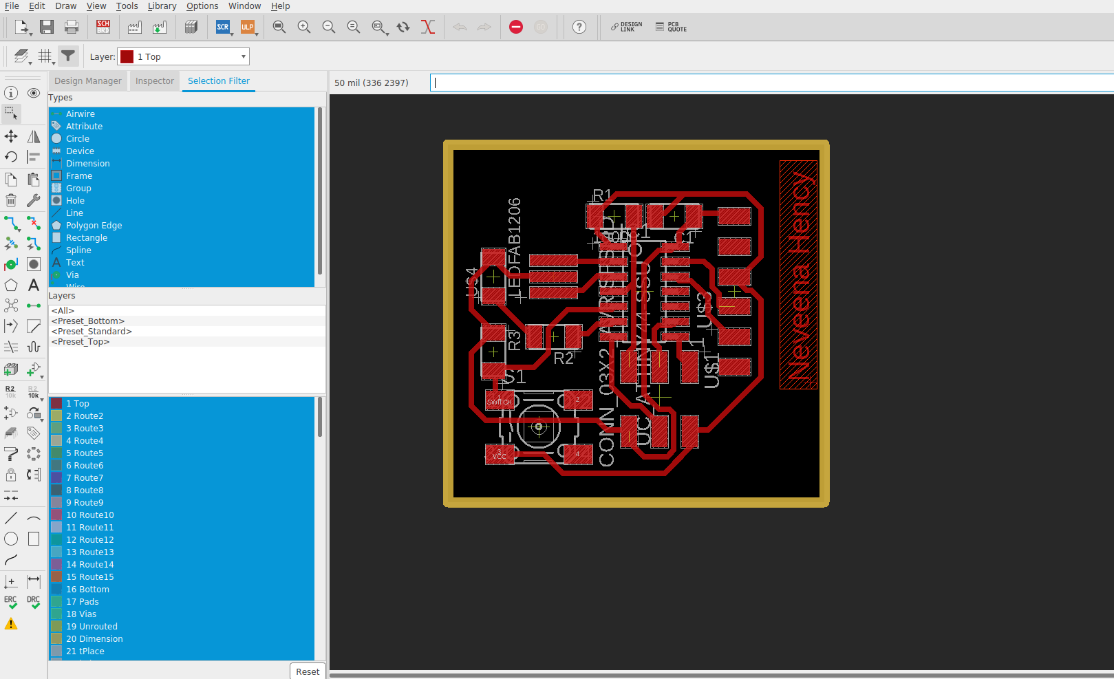
After setting up the schematic we've to design the board.Designing the pcb is the other task.There are certain design rules to be followed before milling the board. we have to consider the machine and material and give those values accordingly.
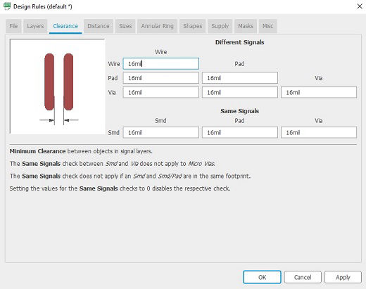 The design rules were changed from the default to the requirements of Modela which is present in our lab.
Start drag and drop the electronics components on the board to black area. Organize the layout of the components,
rotate them and keep what is connected to each other next to each other to make the routing easier later on.
Once components are more or less aligned and as close to their corresponding connections, the traces has to be made using the traces tool.
Click on the center of a component to start a trace, then right-click to change angles.
The design rules were changed from the default to the requirements of Modela which is present in our lab.
Start drag and drop the electronics components on the board to black area. Organize the layout of the components,
rotate them and keep what is connected to each other next to each other to make the routing easier later on.
Once components are more or less aligned and as close to their corresponding connections, the traces has to be made using the traces tool.
Click on the center of a component to start a trace, then right-click to change angles.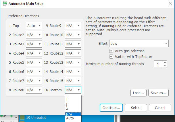
routing is the next step , you can route it in both ways by using autoroute directly from the software or by manually drawing the
routes in the blackboard. Initially i have done autorouting and we get many options from the software itself from that we will have
to choose 100% optimization which gives the near to correct routes but still one of my vcc didnt get connect so tried to draw the lines without
autorouting.
OUTCOME AND REFERENCES
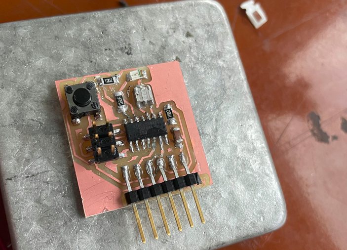
after collecting the components from the inventory room i started soldering the components to milled pcb.
and it looked something like this.