
Week 4
Assignment 1-Make an in-circuit programmer
This week Assignment is to make an in-circuit programmer by milling the PCB. This week we need to build our own ISP(In-system programming),also called in-circuit serial programming (ICSP). To be honest i had least knowledge about how to survive this whole week, but it was way too challenging than i expected everything was new but it turned out to be more interesting and i really enjoyed learning it.
we were introduced to different process to make the pcb
1.To Create and save file of circuit board traces and outcut.
2.To Load a program and module in MODS.
3.1/64 traces files.
4.1/32 holes / outcut file.
5.To Send the files to the machine.
Instead of making a new design we found a isp program from fab foundation.
So this FabTinyISP is the one of the provided designs to mill out the pcb and also learn SMD soldering
WHAT IS ISP (in system programming)?
To program a chip, we will need a special programmer which reads commands from USB to drive the SPI lines to program the chip.SPI stands for Serial Peripheral Interface and is a way for microcontrollers to communicate with each other or with the outside world. It's also called 3-wire sometimes because it uses three wires to communicate.
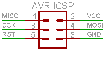
1.VCC - Postive Voltage
2.GND - Ground
3.RST - Reset Pin
4.MISO- Master In Slave Out
5.MOSI- Master Out Slave In
6.SCK - Serial Clock
In here MISO,MOSI, and SCK are the most importent.In SPI system , there will a main Module act as a Master and some peripheral act as Slave.
when master need to send some data/need to communicate with slaves ,the MOSI channel will be activate based on the SCK(Serial Clock),
so the communication will happen in givin Clock time , all the slave will be act as a Input and Master act as Output so the Master can give
Instruction ,like this if the slave need to communicate to the Master they can use MISO that's means the Master can be act as Input and Slaves
will be act as Output ,therefore Slave can give Feedback to the Master .In this week we don't need to design any of the Circuit board , jut need to make our own FabISP verisons.
PCB milling using MODELA MDX20 MACHINE
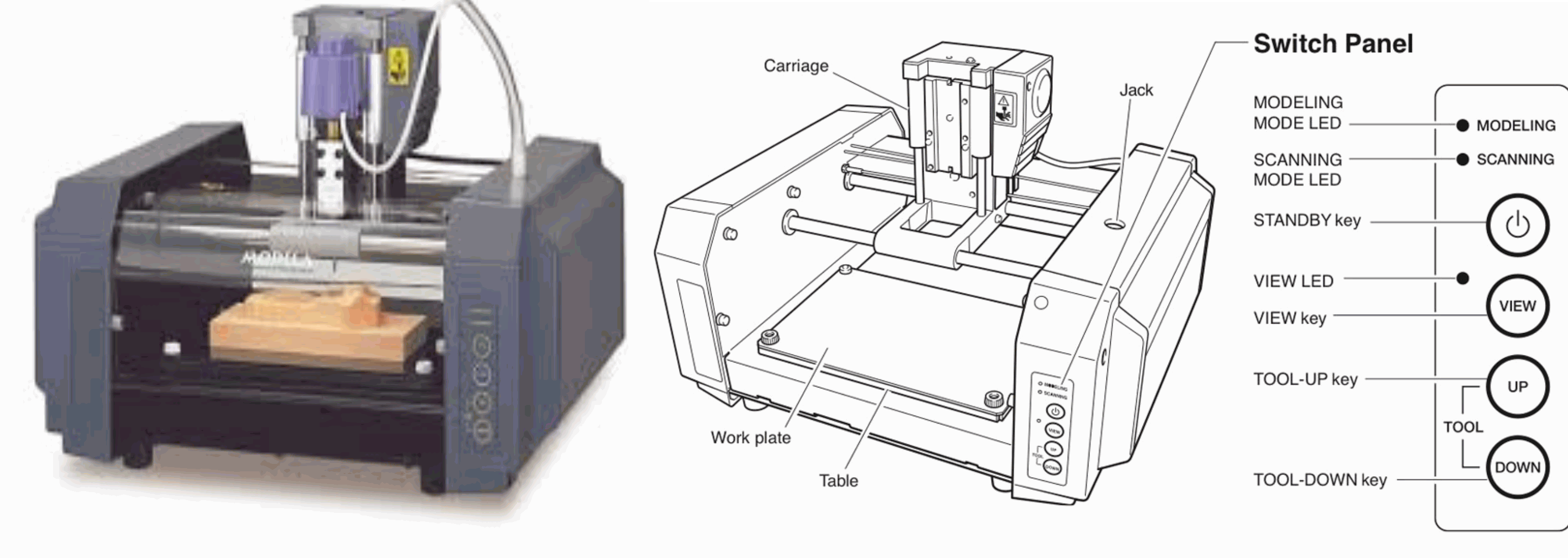
The Roland Modela MDX-20 is a small milling machine and a 2 1/2D precision scanner.
This machine is mostly used for milling circuit boards, though it can also mill in other soft materials like machinable wax.
For milling circuit boards you should export you design into a black&white monocroome png.
For milling out 3 dimensional molds you should export your design as .stl.
The second use of this machine is scanning. It uses a thin needle to gently touch the object and calculates from this a 2 and a half dimensional model.
Though slow at processing, it can create a high detailed model. We use the fab modules to give commands to the Modella and run the cutting program.
This machine is very delicate and the bits are very fragile, take care in removing the milling cutters and correcting the zero setting.
Modella MDX 20 behaves like an ordinary 3-Axis CNC machines, Each axis is driven by a stepper motor and the cutting program tells the machine where to go by giving coordinates to the machine in real time.
We have two milling processes in cutting a PCB, The first one is milling the traces to get the circuit board pattern, and the second is cutting out the board from the base material.
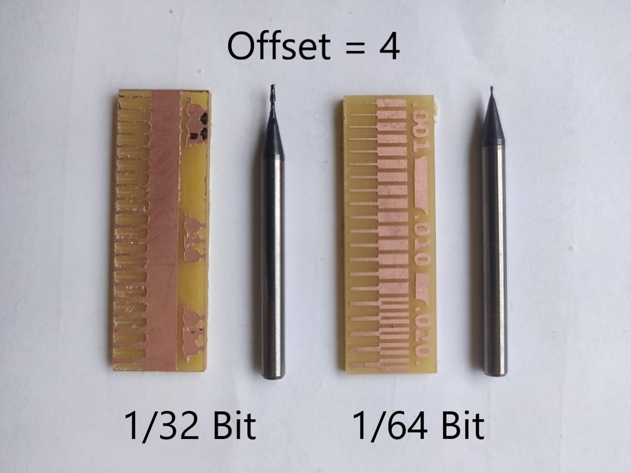
For milling traces, we use the 1/64th inch (0.4mm) bit and for cutting 1/32th (0.8mm) inch bit. The Modela MDX20 is a Desktop 3D scanning and Milling machine by Roland. Easy to use,compatiable with popular softwares, powerful and can directly connect to the computer via RS232C cable.
SPECIFICATIONS.
Maximum Working Area: 203.2 mm (X) x 152.4 mm (Y) x 60.5 mm (Z)
Maximum Table Load Weight: 1 kg (2.2 lbs)
Compatible Materials: ABS,acrylic, wood, plaster, styrene foam,
chemical wood, wax, plaster, polyacetal, ploycarbonate , Sandomur SS , aluminum, brass
Weight of Unit: 13.7 kg (30.2 lbs)
WORKING OF ROLAND MODELA MDX-20
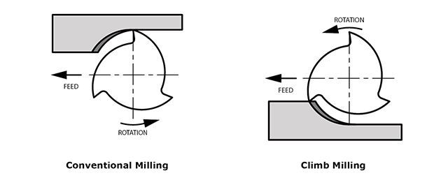
Modella is like an ordinary 3-Axis CNC machines, Each axis is driven by a stepper motor and the cutting program tells the machine where to go by giving coordinates by G.code to the machine in real time. The Fab Module software will convert .png image in to a we series of tool paths, these tool paths are defined by their coordinates and G-code. The .png image is a black and white layout of the board, and the black portions will be milled and the white portion is where the copper will be left. We have two processes in making a PCB, The first one is milling the traces to get the circuit board pattern, and the second is cutting out the board from the base copper clad. For milling traces, we use the 1/64th inch (0.4mm) bit and for cutting 1/32th (0.8mm) inch bit.i'll examplain all things one by one. We also discussed about the types of milling.
FABRICATION OF FAB FabTinyISP
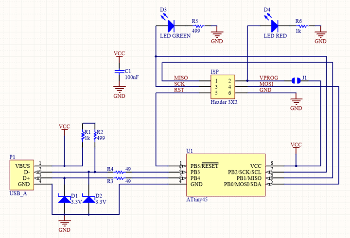
I,am Using FabTiny ISP Documentaion and Source file by Brian Mayton and we can get all the resource here. FabTinyISP
Below shows the schematic and position diagram respectively.
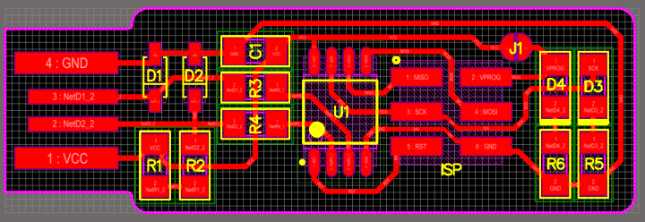
SETTING UP THE MACHINE.
1.First Make sure to use some Sacrificial material on top of the bare metal base ,
it will prevent the damage of bit or the machine’s table.
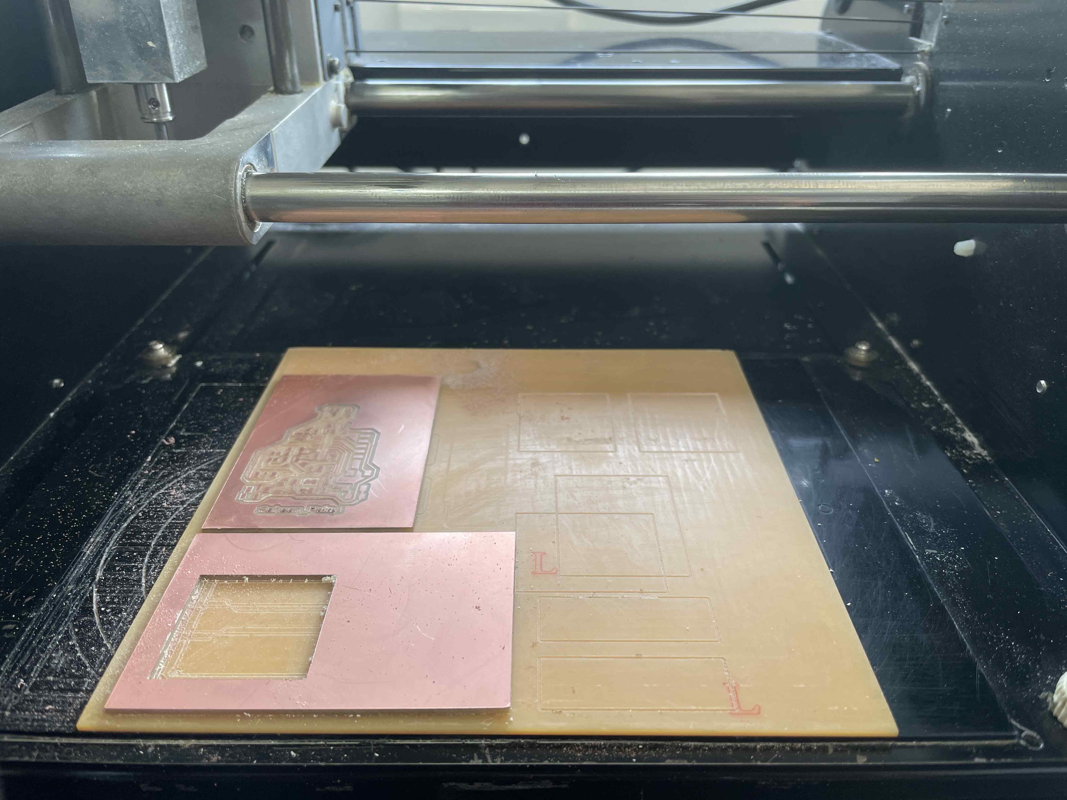
2.Check the Drilling bit's , first we need mill the trace then cut,and make sure to use the correct bit.
when we start to mill trace check the bit because the previous person will cut his board with cutting bit and
that will be the default when we start to work.
3.Fix the PCB on top of the Sacrificial layer, better to use a double sided tape
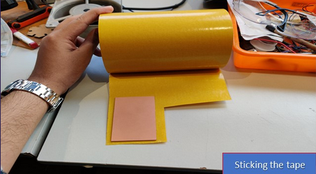
4.For tighten the bit ,first click view then the table should come out and the head will move to the far right,now load the bit you want to use, for milling traces,
we use the 1/64th inch bit and for cutting 1/32th inch bit. Now insert the bit and use the Allen key to tighten the screw. Make sure it is tight on both sides.
5.For Move the (0,0) Position click the View mode again.
6.Now Set the X'axis and Y'axis for by clicking on move to Xmin and Ymin on the Fab Module.
7.Set Z'axis by using Up and Down on the Control panel.
8.Before starting Milling check your speed and depth settings and the tool position on the fab modules window.
PCB FABRICATION.
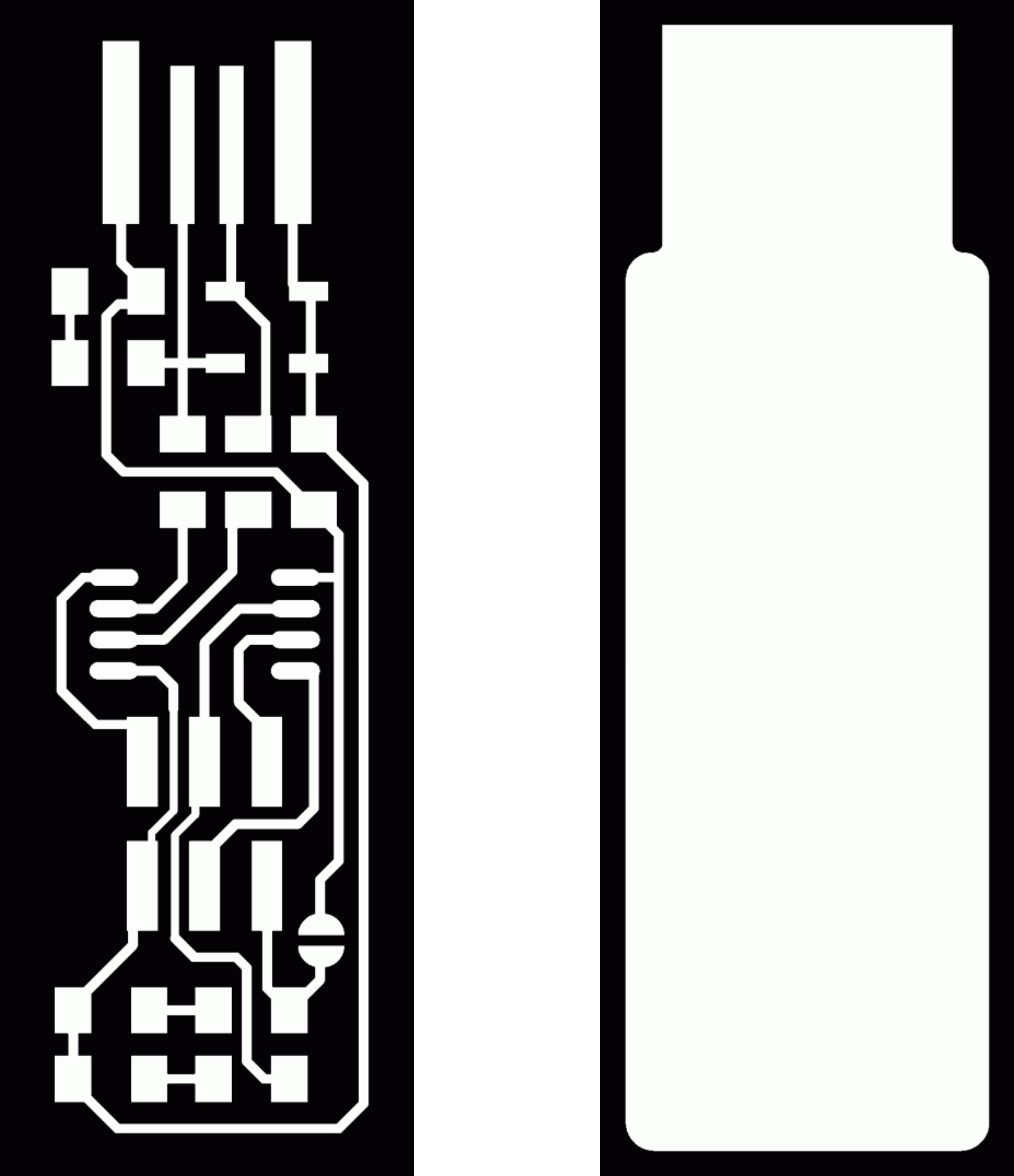
My PCB trace was vertically oriented and the above image shows the traces and outline cutout.
Like the vinyl cutter you have to conduct the following steps to setup MIT Mods.
1.First you need to go to Mods folder and must open terminal there by using right click.
2.Then you need to type bash start-servers which would open MIT Mod interface.
3.Now you need to select MDX Mill and select PCB to access the Mod workflow.
Then you need to export the drawings to the MODS. Always mill out the Traces first using the 1/64 bit and change the tool to 1/32 bit and position the tool
to the same origin used for tracing. Afer importing the image you need to calculate the bit and calculate raster.
Ensure that you trace first followed by cutting. Once calculation is complete you can verify the tool path by selecting the view command.
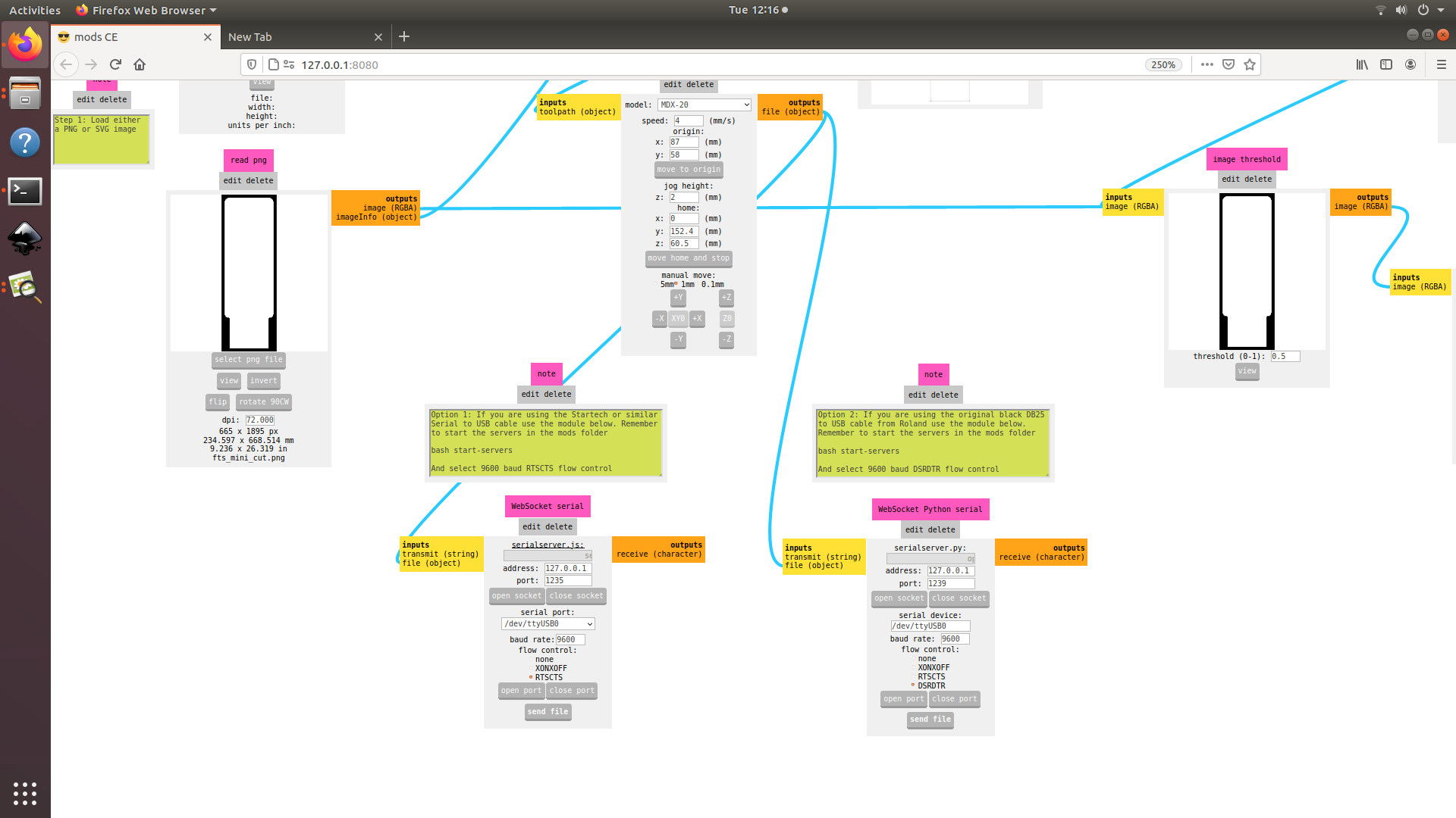
Next you need to set the origin by going onto suitable coordinates referred from the work area in the milling machine and don't ever forget to
remember/screenshot the X & Y coordinates. You can repeat the same process for cutting as well but make sure that you use 1/32 bit and ensure
that the origin coordinates are alike.
We are using FR-1 Grade PCB.
open Fab Modules by typing fab on linux terminal or you can use the online version.
In Fab Module Select Image(.png) as Input and Roland MDX-20 mill(rml) as ouput Process and Click make_png_rml .
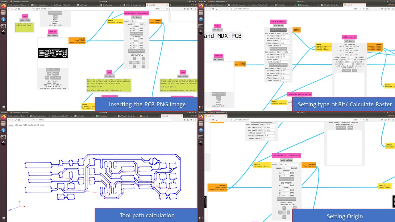
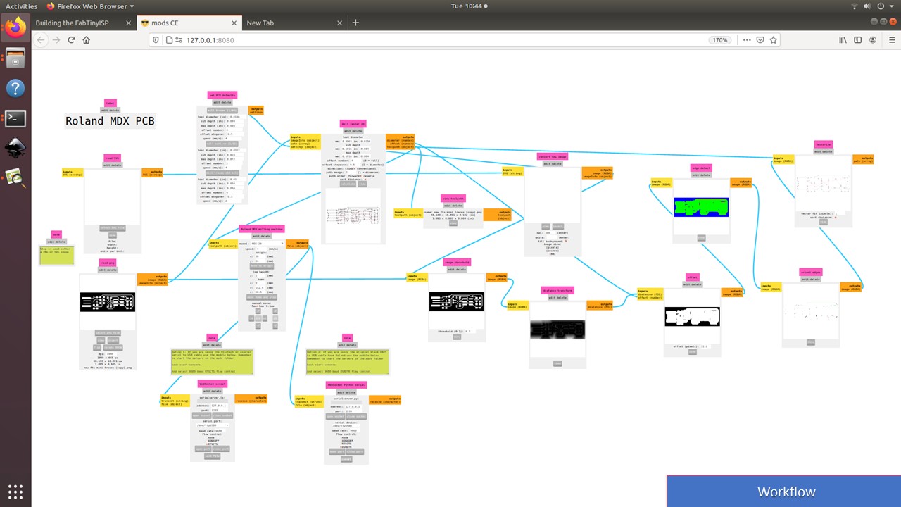
while i was milling i came through some errors on setting the dpi.
SOLDERING.
i have no exerience in Through hole soldering , but here we are going to handle SMD (Surface Mount Devices) components.
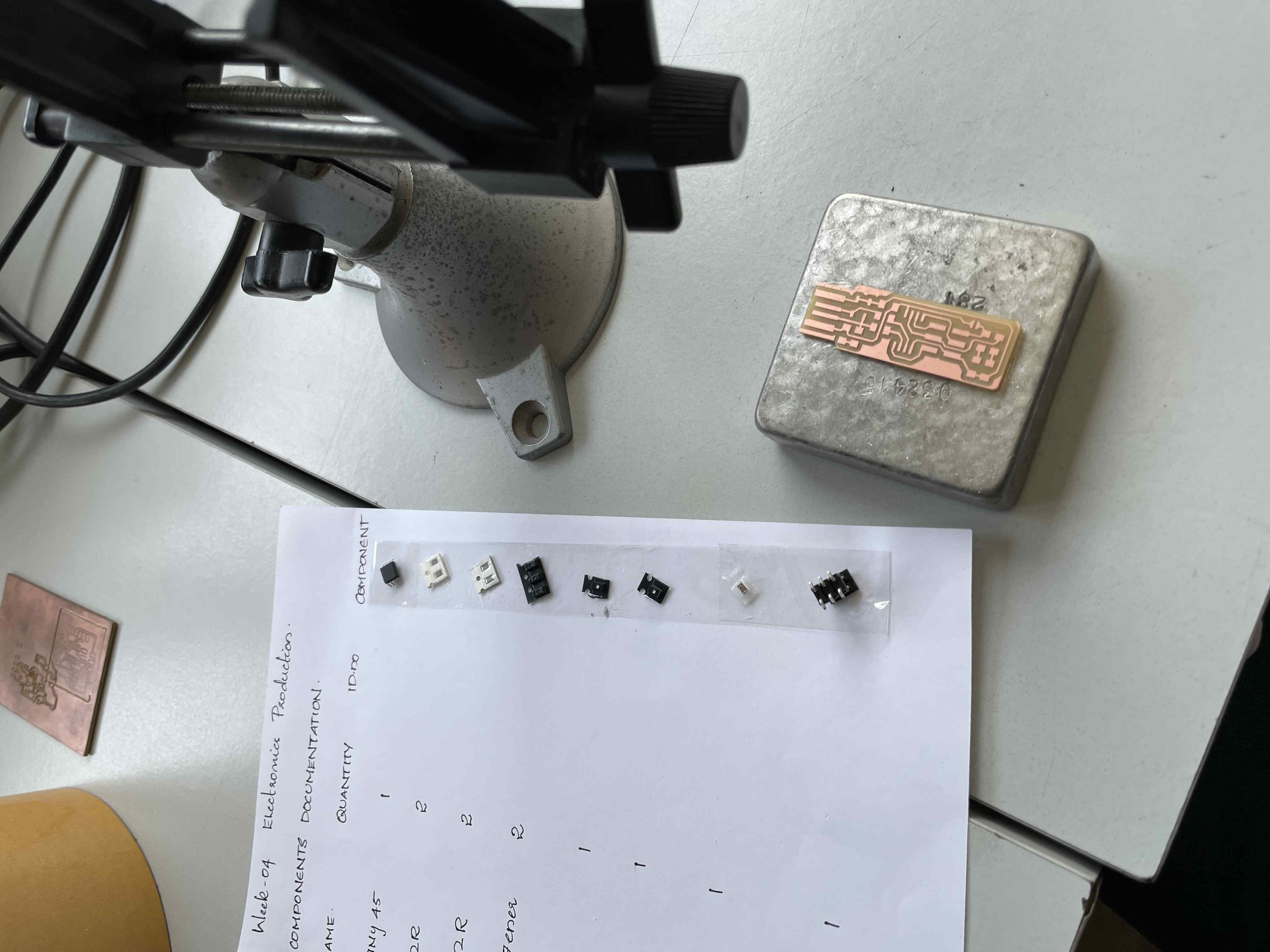
First i Collected all the component that we need to build our ISP
1x ATtiny45 or ATtiny85
2x 1kΩ resistors
2x 499Ω resistors
2x 49Ω resistors
2x 3.3v zener diodes
1x red LED
1x green LED
1x 100nF capacitor
1x 2x3 pin header
PROGRAMMING THE PCB.
Before programming its ideal to check the board against the schematic and pcb layout image to make sure that you have installed the correct components in the correct locationa dn orientations.it should not be flat on the board or not tilted with pins in the air make sure the solder connections to be smooth and flowed both into the pin and pad. Atlast use multimeter to check for shorts between vcc and gnd.
Before building up and to program the firmwire onto the board, we need to setup the development environment.
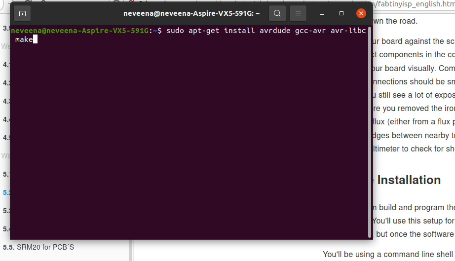
for ubundu users enter the following command.
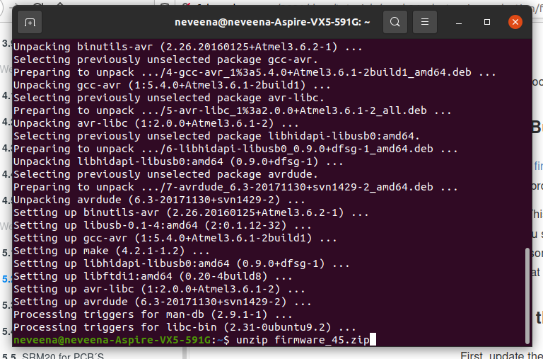
sudo apt-get install avrdude gcc-avr avr-libc make.
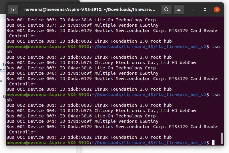
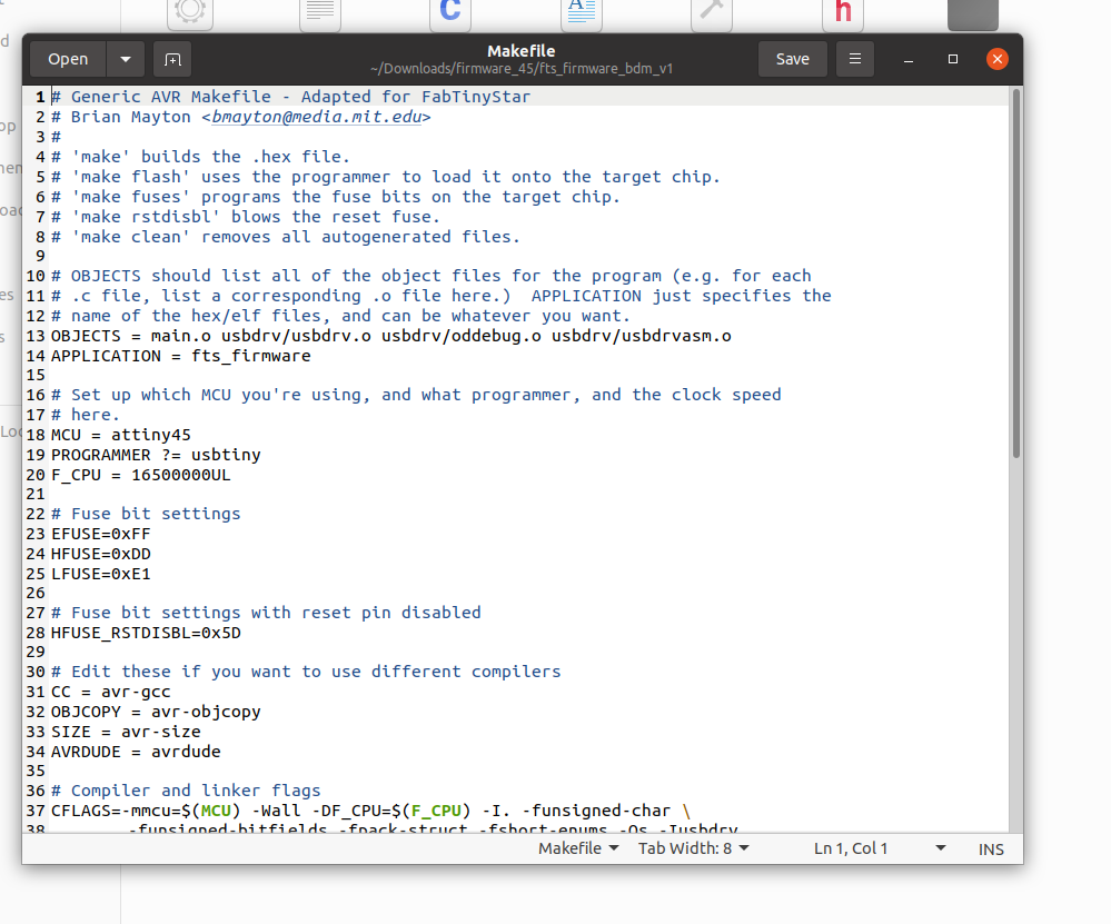
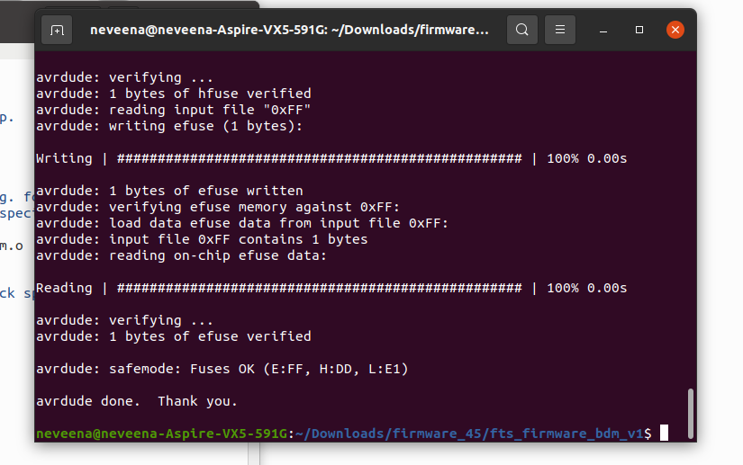
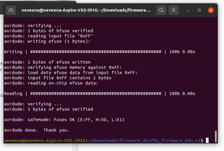
open the terminal program and cd into the source code directory. Run "make".This will build the hex file that will get programed onto the ATtiny45. When the command completes we will have a file called "fts_firmware.hex".
OUTCOME AND REFERENCES
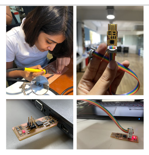 The device was successful.
