Week 6: Electronics design
For PCB design I personally like KiCad workflow, it doesn't have a polished interface like Eagle or Altium Designer but I prefer it because it is free and accessible to anyone, no need to create an account or pay a monthly subscription.
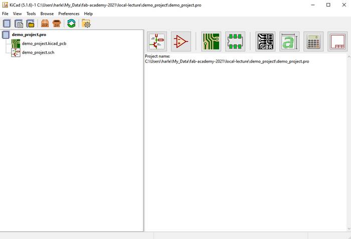
KiCad more than a simple software is a collection of softwares and tools that work together for PCB design. The whole process starts by creating a KiCad project that contains the rest of the files, initially the project will start with a schematic and circuit board editor.
The program in charge of editing the schematic is called Eeschema and it is used to create the connection diagram of the components that make up the circuit. To add a component it is necessary to open the library that is located on the right side panel.
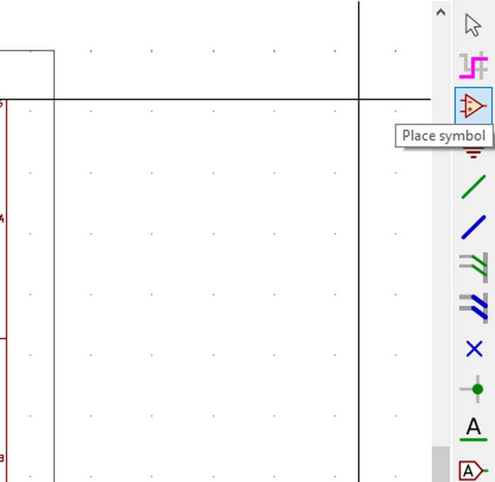
In the search engine you can search for a specific component or a specific library, for example a resistor.
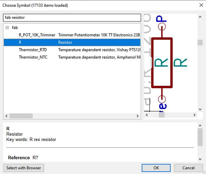
With the component selected, press Ok and place the element in the workspace.

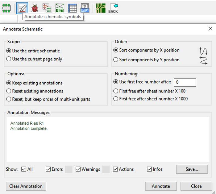
Then it is necessary to reference the components with a unique name, in KiCad it is called "Annotate" and assigns a unique identifier to each symbol.
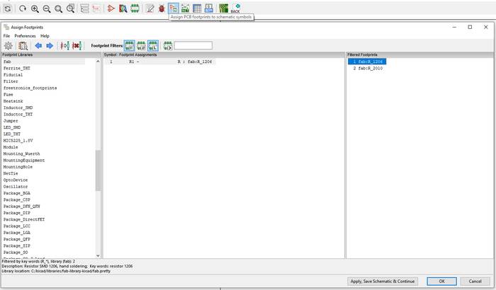
For example a physical resistor can have a great variety of shapes and sizes, the components that are added in the schematic need to be associated with a physical shape, this is known as a footprint. KiCad has a collection of footprints that can be accessed from the top menu "Assign PCB ...".
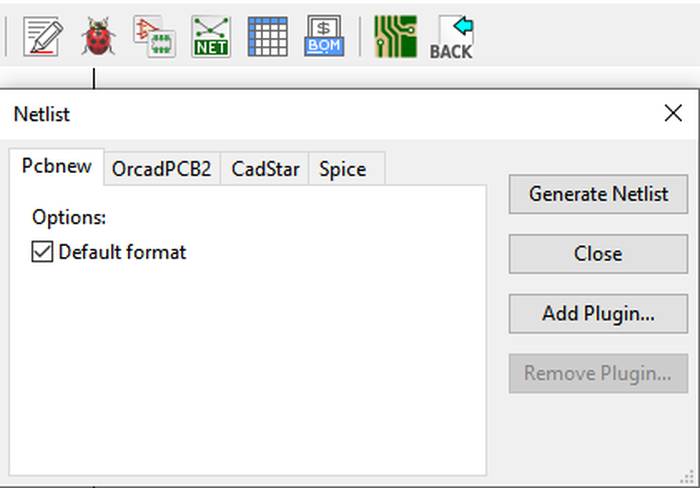
At this point you can consider the schematic design as finished, but the PCB editor "Pcbnew" does not yet know the components in the schematic. For what is in the schematic to be used in the editor it is necessary to create a "Netlist" that basically associates the symbols to their respective footprint so that "Pcbnew" can use them, at the top there is a button "Generate Netlist".
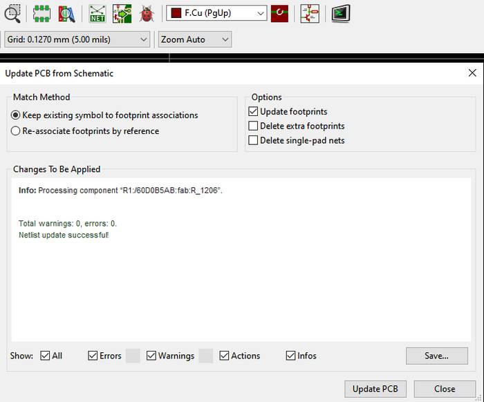
Now in the main window of the KiCad project or in the upper part of Eeschema you can open Pcbnew. In this workspace it is necessary to go to the upper part that says "Update PCB from schematic", it will open a reminder that when you click on the "Update PCB" button KiCad uses the previously generated Netlist to place all the components. Now any changes made to the schematic are updated (manually, NOT automatically) in Pcbnew.
For a detailed step-by-step tutorial for the PCB layout process, see Fab Motor controller
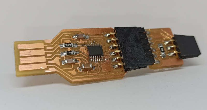
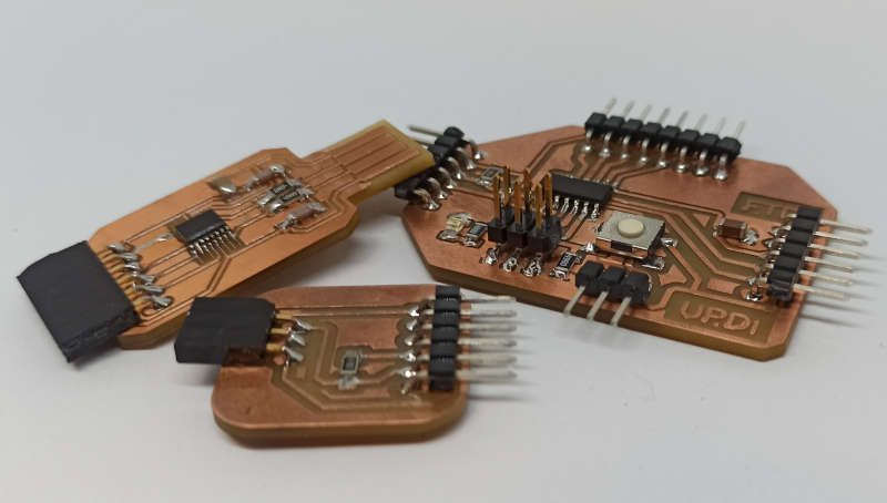
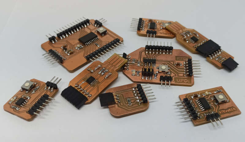
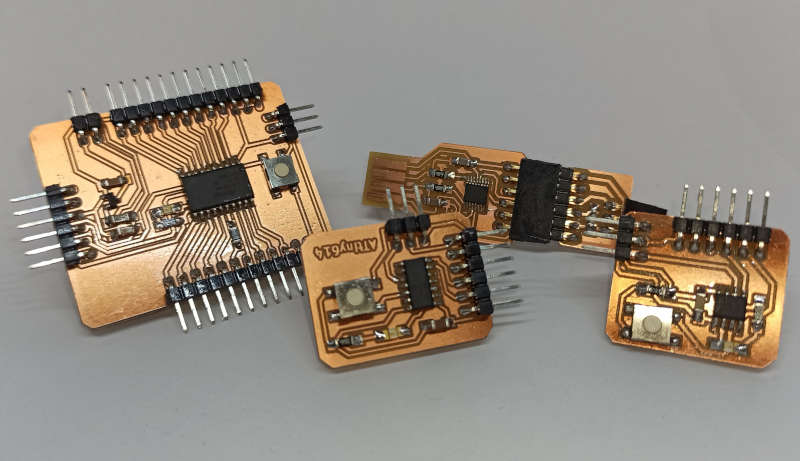
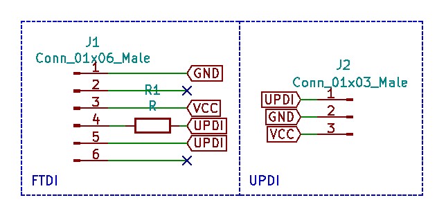
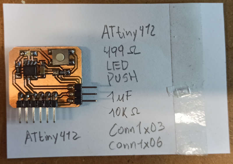
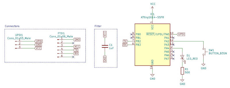
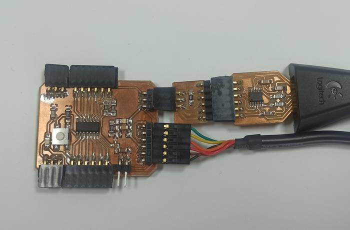
In this assignment I decided to design 3 circuit boards with the requirements of a button and a LED, the microcontrollers used are: ATtiny412, ATtiny1614, ATtiny3216. This group of microcontrollers can be programmed by SPI or UPDI, in this case during the whole FabAcademy I am going to work only with UPDI so it is necessary a small board with a 4.7k Ohm resistor that serves as an interface to program all the micro-controllers mentioned above.
The schematic is very simple, it illustrates the FTDI to UPDI connections that allow to load the program to the controllers.
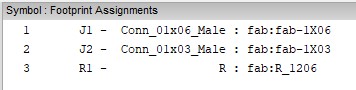
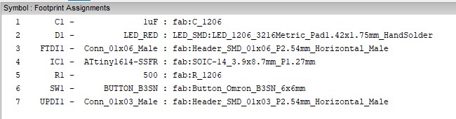
The components used correspond to:
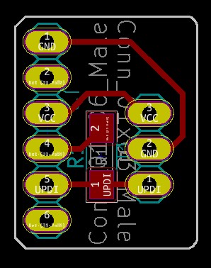
The routing of the board looks as follows:
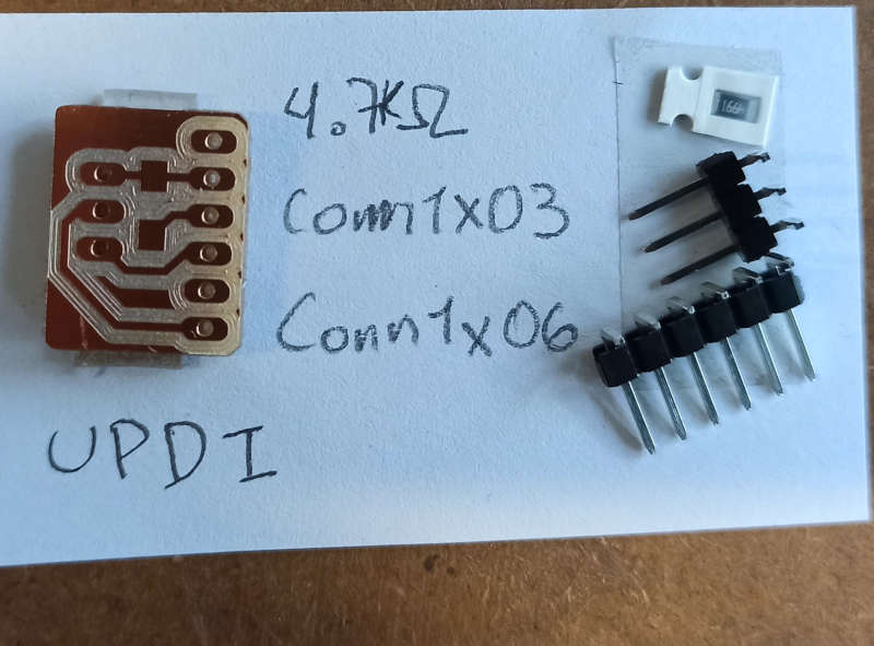
After generating the G-code to mill the board the physical components to be soldered are:
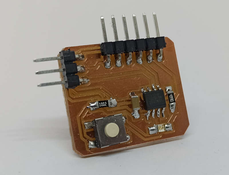
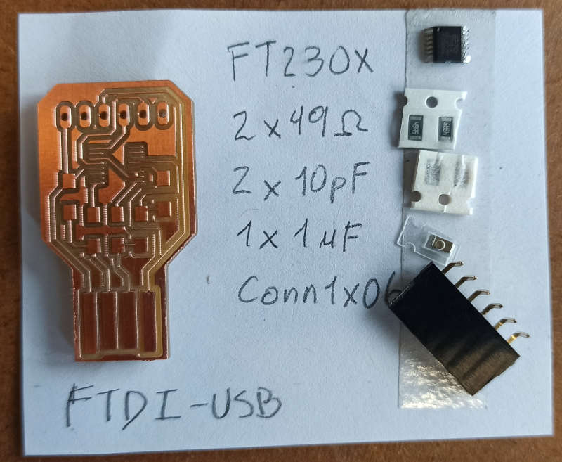
The previous board by itself does not work, it must be complemented with another one that works as an interface between the computer and the UPDI to be more specific it must convert from USB to Basic UART IC, just that is the function of the FT230X chip.
The schematic looks like this:
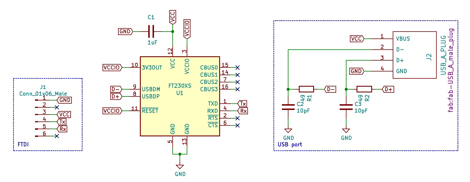
On the left side are the FTDI connection pins that go to the UPDI board designed earlier.
On the right side is the USB interface that connects to the computer.
And in the central part the connections to the chip.
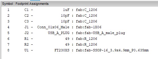
The components used on this board are the following:
The pcb routing looks like this:
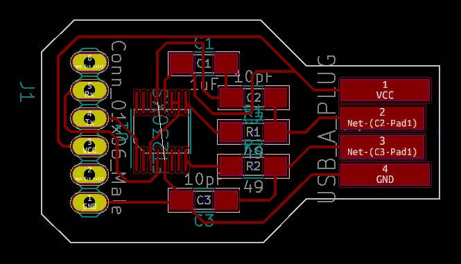
As a clarification there is a GND connection that seems to be incomplete but the chip internally has them connected so it is not necessary an external physical connection.
These with the physical components ready to be soldered:
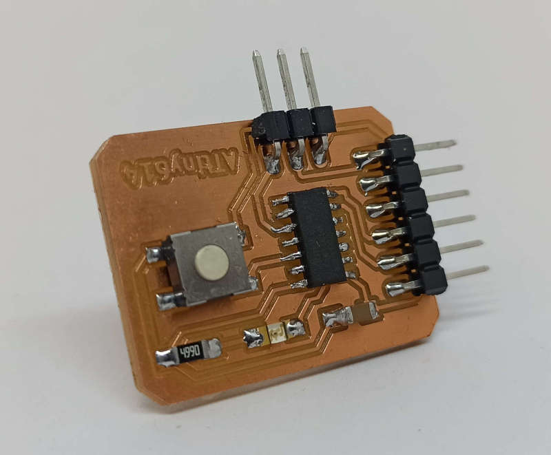
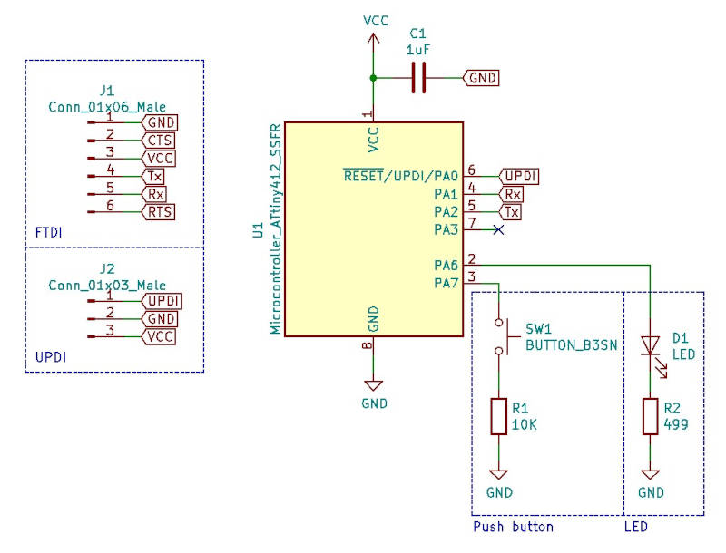
The following PCB uses the smallest micro-controller of the 3 I am using, the schematic is as follows:
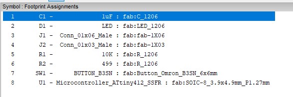
The list of components:
The PCB routing:
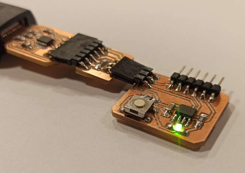
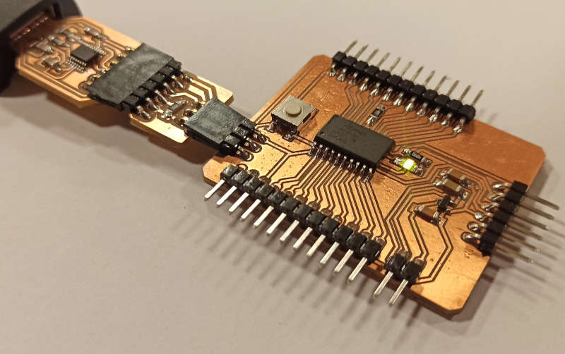
After soldering the physical components you get this.
Testing the operation.
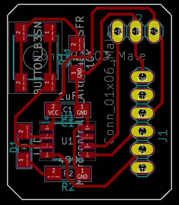
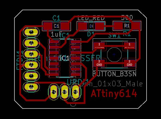
The following pcb uses the ATtiny1614 micro-controller, the schematic of the connections are as follows.
The list of components used are:
The final routing was as follows
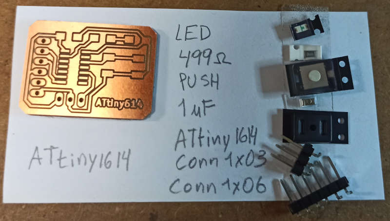
The physical components to be used are shown in the following image
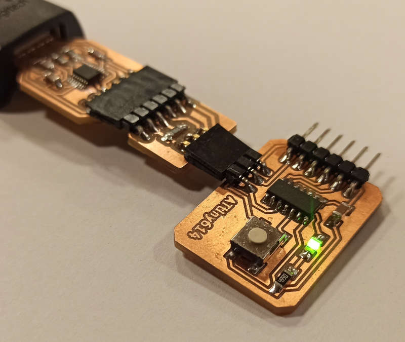
Testing in operation
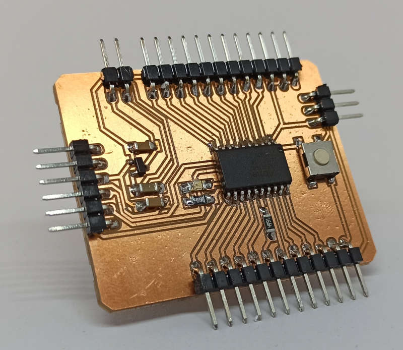
The last PCB uses the ATtiny3216 micro-controller. The schematic corresponds to the following image.
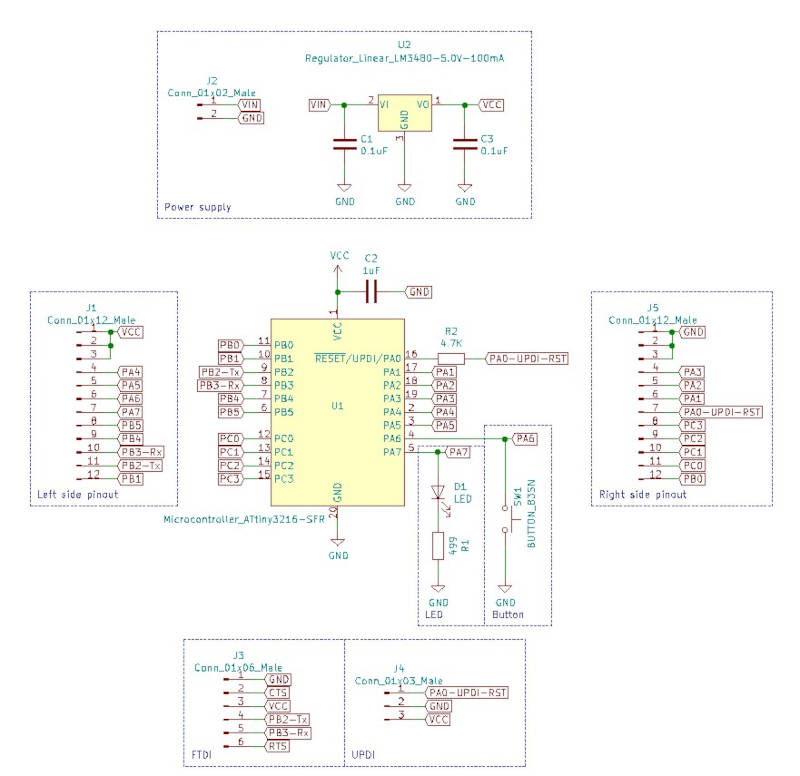
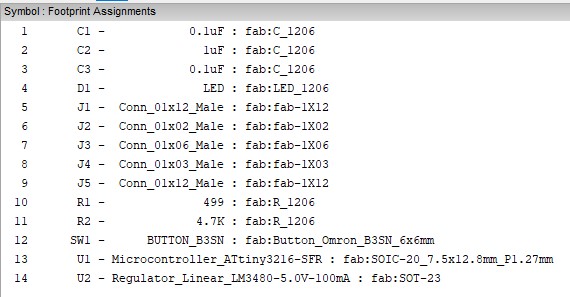
The list of components is:
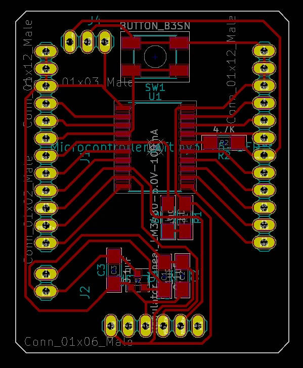
The final routing was as follows
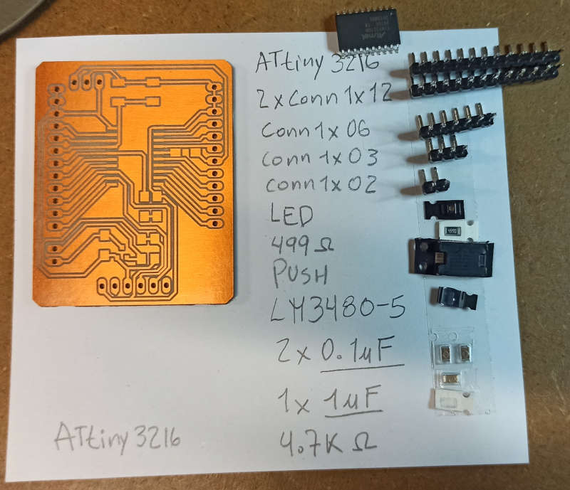
The physical components to be used are shown in the following image
Testing in operation
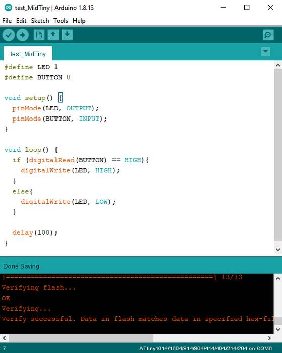
The test program:
#define LED 1

void setup() {
  pinMode(LED, OUTPUT);
}

void loop() {
  digitalWrite(LED, HIGH);
  delay(100);
}
All the PCBs described above use the same design rules. They all use a 0.4mm trace width which for the pins of these microcontrollers using a 14-SOIC package is neither too wide nor too thin.
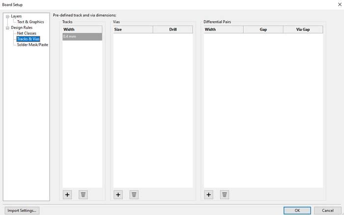
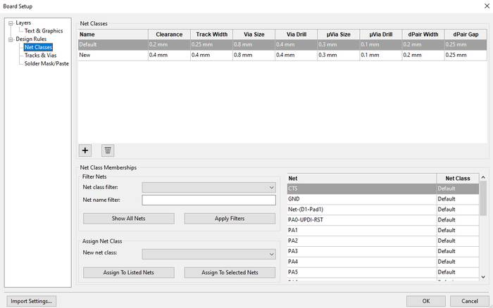
The next thing was to create a Net Class called "New" where the most important parameters are "Clearance" 0.4 mm and "Track Width" 0.4 the rest of them are not relevant because they are not being used. With the Clearance a space between each Track is ensured but because a V-End Mill of 0.2 to 0.5mm was used to mill these PCBs the value of 0.4mm is within the range.
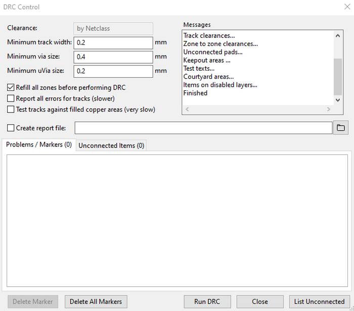
Now it is necessary to run the "Design Rules check" to make sure that everything is as it should be.
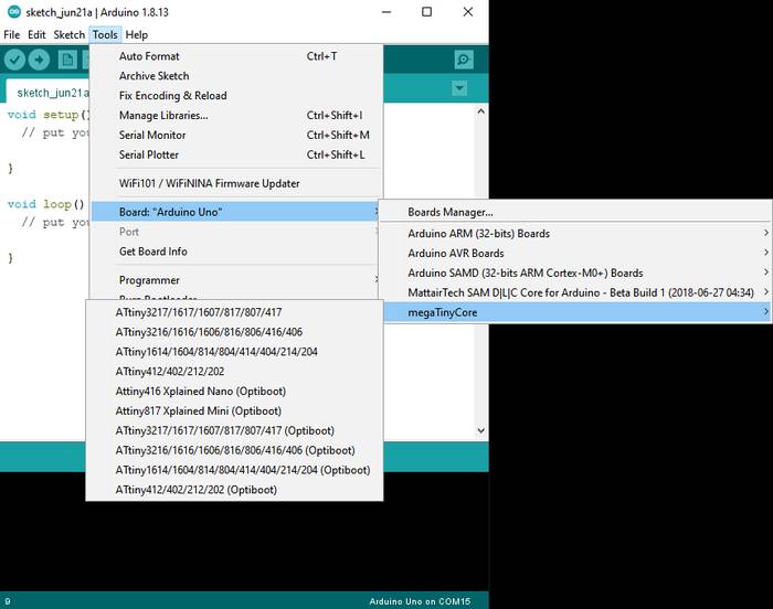
To program all the boards you need to install the Arduino Core for the tinyAVR 0/1/2-series family, which can be found on github as megaTinyCore.
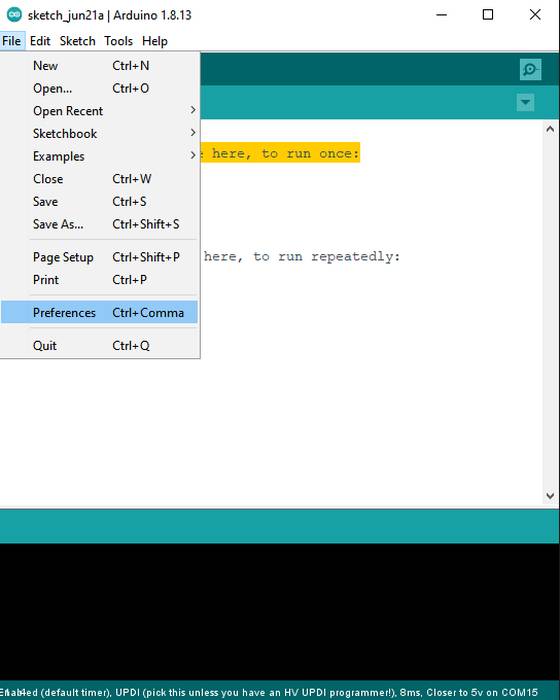
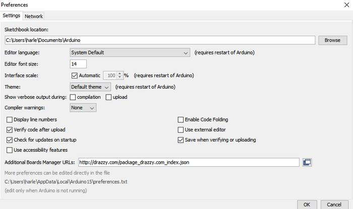
To install the megaTinyCore it is necessary to open the Arduino IDE and go to File->Preferences
In the box "Additional Boards Manager URLs" paste the link http://drazzy.com/package_drazzy.com_index.json
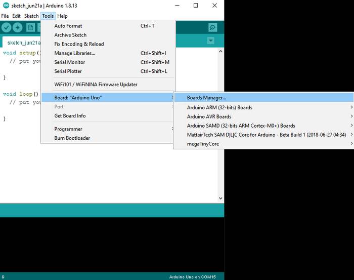
With that link added you can now search and install the library that contains the Arduino Core for these boards. You have to go to Tools->Board:->Boards Manager...
A window will open where you have to search for "megaTinyCore" and press the install button.
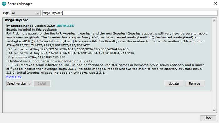
If the installation was successful you will see a new collection of boards.
Before uploading the code it is necessary to connect the PCB using the UPDI board and the FT230x, you can also add a FTDI cable to view data on the console. For this example we will use the PCB I call MidTiny.
The test code consists of turning on the integrated LED on the board by pressing the button also integrated.
The necessary configurations to upload the code correctly are shown in this image.
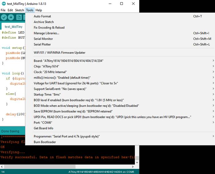
Finally it is a matter of pressing "Upload" in the Arduino IDE.