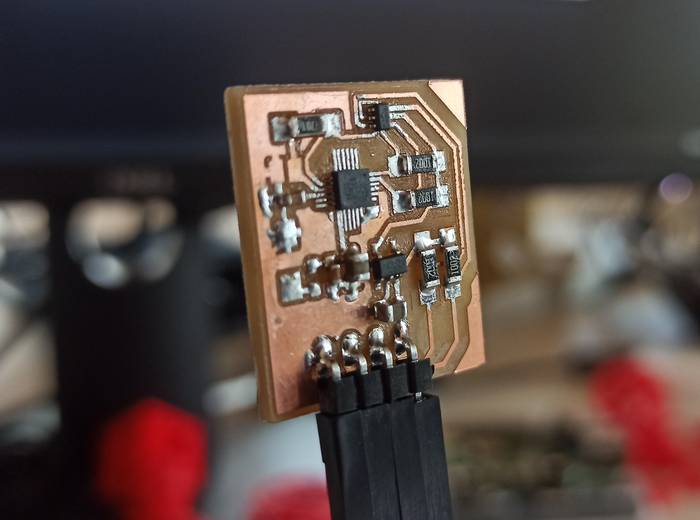
Fab IMU
The Fab IMU is a 9 degrees of freedom sensor that includes a 3-axis gyroscope, 3-axis accelerometer, 3-axis compass and a temperature sensor, all thanks to the ICM-20948 chip.
The schematic is composed of several sections, one of them is the voltage regulator, because the chip works at 1.8V it is necessary to decrease the input voltage from 5v to 1.8V.

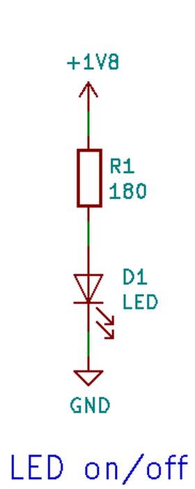
It includes an indicator led placed after the voltage regulator to show the status of the sensor.
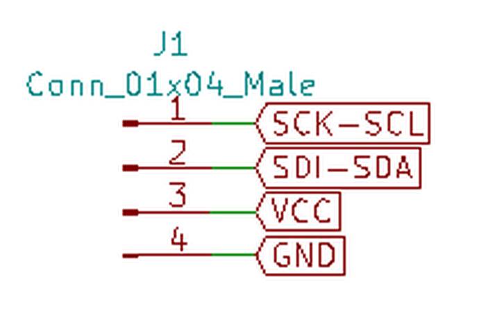
The communication interface is I2C so the exposed pins correspond to SCL, SDA, VCC and GND.
The logic voltages of SCL and SDA should be 1.8V because I am using a BSS138DWQ-7 which consists of a pair of MOSFETs that allow pull-up and shift.

The last section of the schematic is the chip that is connected like this.

An image of the complete schematic is this one.

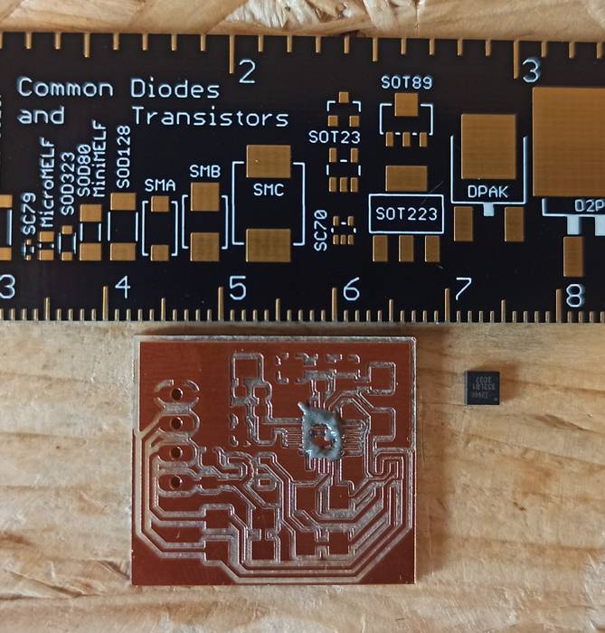
The pcb layout looks like this.
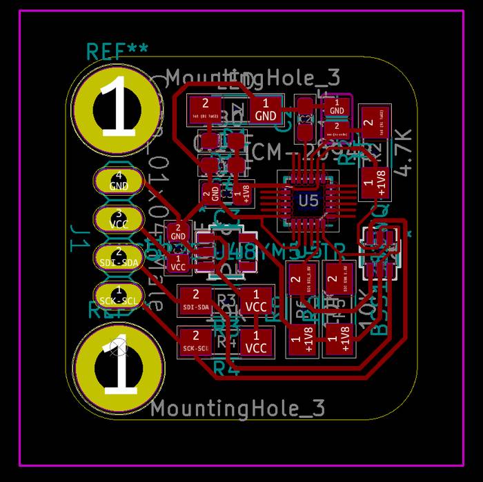
As you can see the chip has some pins that are not connected, but due to the small size I added some tracks that extend the contact surface, this in order to facilitate the soldering process of the chip.
The sizes of the tracks that are connected to the chip are 0.2 mm, the others are 0.3 mm.
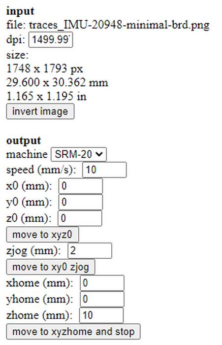
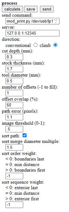
The milling process is similar to the previous processes described in my documentation, only some parameters change in the G-code generation process.
Before that it is IMPORTANT to note that the values shown below are based on the hardware with which the pcb is milled. The machine that performs the work is a SRM-20 with an End-mill V-Tool of 0.2-0.5mm that performs all the work (traces, holes and cuts), by the characteristics of the End-mill and after many tests I am sure that these values give a very good result in quality and time. If you have a different machine and a different end-mill better use the values you are used to use or do some tests to find the ones that fit better. You can see a video of this end-mill at 20mm/s on a MDX-40 here.
Traces, machine output
Traces, process
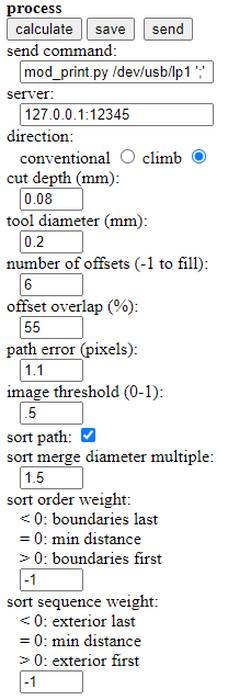
Holes, machine output
Holes, process
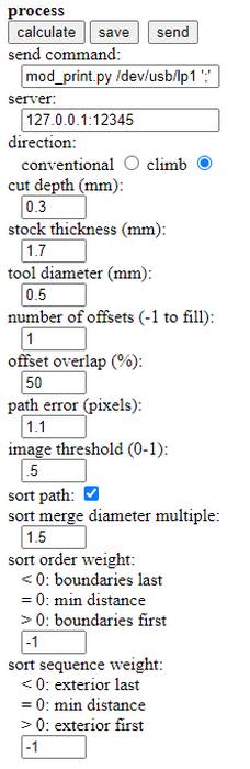
Cutout, machine output
Cutout, process
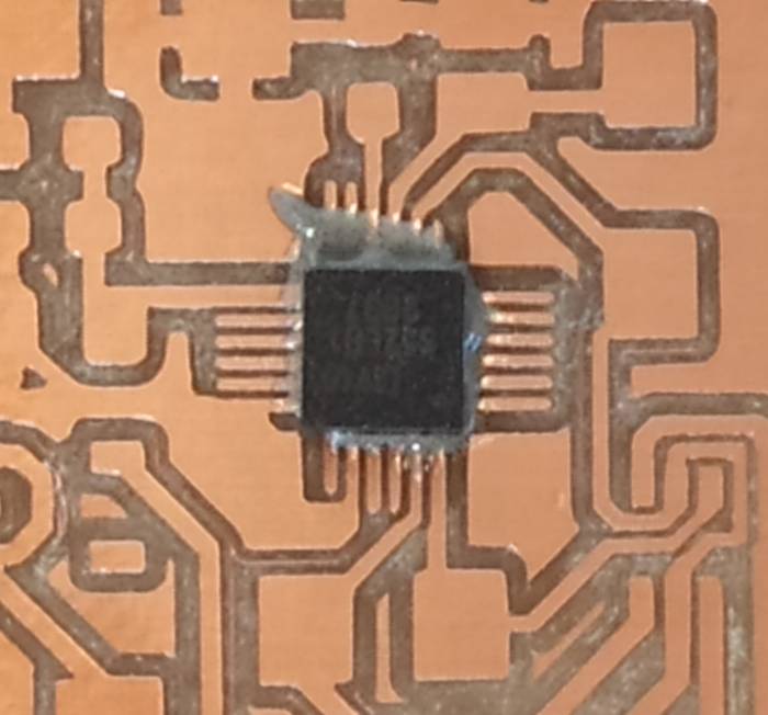
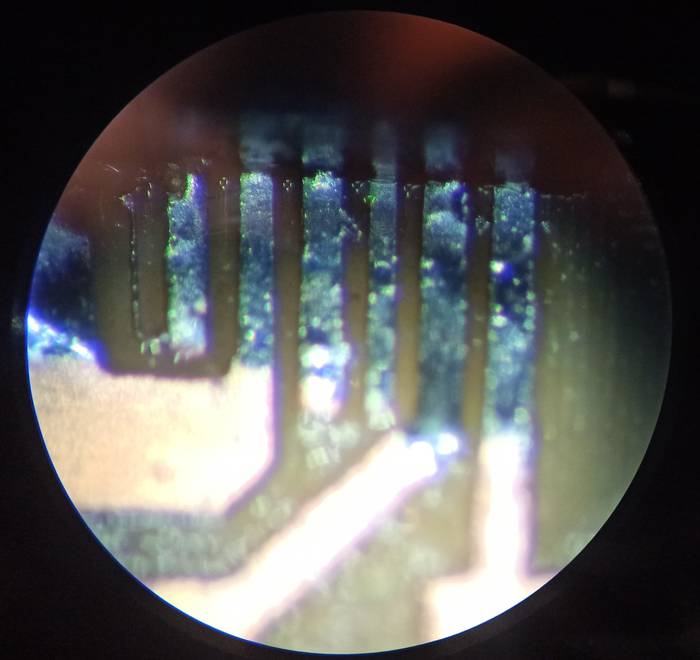
The chip has a 24-pin QFN 3x3x1mm package which is very difficult to solder by hand and practically impossible to solder by eye alone. You need some kind of magnification system like a magnifying glass or a microscope.
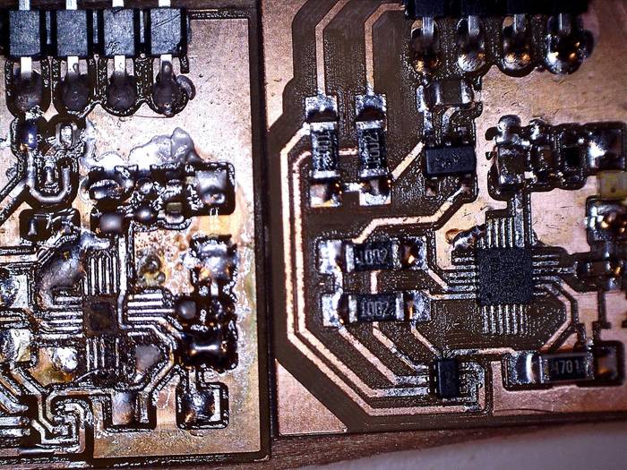
Initially I tried to solder with the naked eye using solder paste and a hot air gun.
This method has some problems as it is difficult to align the chip to the tracks and the result after the paste melts is not very clean.
This method that uses solder paste is more advisable to use it in pcb that have solder-mask since it avoids the dirty result that is produced in a pcb that has all the copper exposed.
After some time trying to do the soldering process with the naked eye we noticed that it was very difficult to align the pins of the chip with the tracks, so we got a microscope to make the job easier to observe.
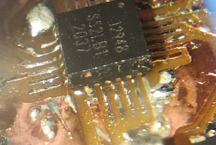
But now the soldering method to use was different. First I applied a thin layer of solder on the tracks where the chip will be placed, then I put some solder on the pins of the chip, aligned the pins to the tracks and placed the tip of the soldering iron heated to 385 degrees Celsius and thanks to the heat transfer between the track and the pins the chip was perfectly in place.
A comparison between the first attempt (left) and the second (right).